

Page 1
Vishay Telefunken
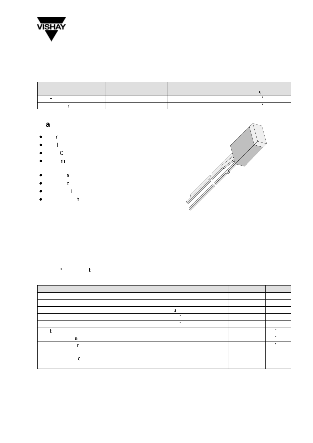
Bicolor Symbol LED
in 2.5 x 5 mm Untinted Top-Diffused Package
Color Type Technology Angle of Half Intensity
High efficiency red TLSV5100 GaAsP on GaP 50
Green TLSV5100G GaP on GaP 50
Features
D
Even luminance of the emitting surface
D
Ideal as flush mounted panel indicators
D
For DC and pulse operation
D
Color mixing possible due to separate
anode terminals
D
Luminous intensity selected into groups
D
Categorized for green color
D
Wide viewing angle
D
Common cathode
TLSV5100
±
ö
°
°
96 11496
Applications
Indicating and illumination purposes
Absolute Maximum Ratings
T
= 25_C, unless otherwise specified
amb
TLSV5100 ,TLSV5100G ,
Parameter Test Conditions Symbol Value Unit
Reverse voltage per diode V
DC forward current per diode I
Surge forward current per diode tp ≤ 10 ms I
Power dissipation per diode T
Total power dissipation T
Junction temperature T
Storage temperature range T
Soldering temperature t ≤ 5 s,
Thermal resistance junction/ambient per diode R
Thermal resistance junction/ambient total R
≤ 55°C P
amb
≤ 55°C P
amb
2 mm from body
R
F
FSM
V
tot
stg
T
sd
thJA
thJA
6 V
30 mA
1 A
100 mW
150 mW
j
100
–55 to +100
260
450 K/W
300 K/W
°
C
°
C
°
C
Document Number 83052
Rev. A1, 04-Feb-99
www.vishay .de • FaxBack +1-408-970-5600
1 (6)
Page 2
TLSV5100
Vishay Telefunken
Optical and Electrical Characteristics
T
= 25_C, unless otherwise specified
amb
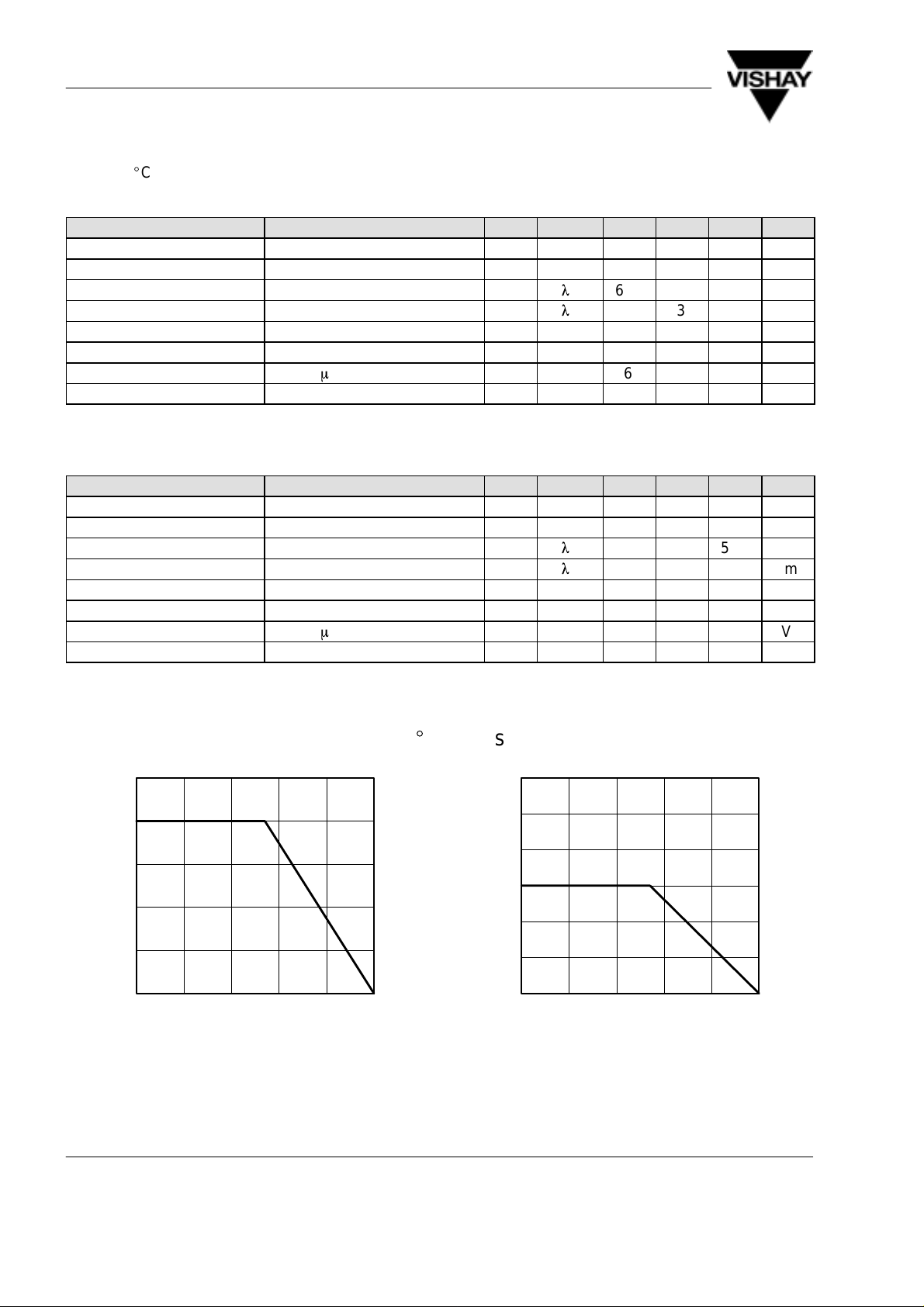
High efficiency red (TLSV5100 )
Parameter Test Conditions Type Symbol Min Typ Max Unit
Per diode
Luminous intensity IF = 10 mA, I
Vmin/IVmax
Dominant wavelength IF = 10 mA
Peak wavelength IF = 10 mA
Angle of half intensity IF = 10 mA ϕ ±50 deg
Forward voltage IF = 20 mA V
Reverse voltage IR = 10 mA V
Junction capacitance VR = 0, f = 1 MHz C
Green (TLSV5100G )
Parameter Test Conditions Type Symbol Min Typ Max Unit
Per diode
Luminous intensity IF = 10 mA, I
Vmin/IVmax
Dominant wavelength IF = 10 mA
Peak wavelength IF = 10 mA
Angle of half intensity IF = 10 mA ϕ ±50 deg
Forward voltage IF = 20 mA V
Reverse voltage IR = 10 mA V
Junction capacitance VR = 0, f = 1 MHz C
≥ 0.5 I
≥ 0.5 I
0.63 1 mcd
V
l
l
V
l
l
612 625 nm
d
p
F
R
j
635 nm
2 3 V
6 15 V
50 pF
0.63 1 mcd
562 575 nm
d
p
F
R
j
565 nm
2.4 3 V
6 15 V
50 pF
Typical Characteristics (T
125
100
75
50
V
25
P – Power Dissipation ( mW )
0
020406080
T
95 9983
Figure 1 Power Dissipation vs. Ambient Temperature
www.vishay .de • FaxBack +1-408-970-5600 Document Number 83052
2 (6)
– Ambient Temperature ( °C )
amb
= 25_C, unless otherwise specified)
amb
60
50
40
30
20
F
I – Forward Current ( mA )
10
100
0
020406080
T
95 9984
Figure 2 Forward Current vs. Ambient Temperature
– Ambient Temperature ( °C )
amb
100
Rev. A1, 04-Feb-99
Page 3
TLSV5100
Vishay Telefunken
10000
tp/T=0.01
1000
0.02
0.05
0.1
100
0.2
0.5
1
10
F
I – Forward Current ( mA )
T
amb
1
0.01 0.1 1 10
t
95 10085
– Pulse Length ( ms )
p
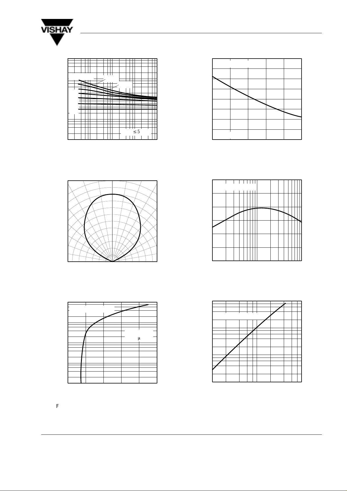
Figure 3 Forward Current vs. Pulse Length
0°
10°20
1.0
0.9
v
55°C
1.6
High Efficiency Red
1.2
0.8
0.4
v rel
I – Relative Luminous Intensity
100
95 10027
IF=10mA
0
0
20 40 60 80
T
– Ambient Temperature ( °C )
amb
100
Figure 6 Rel. Luminous Intensity vs.
Ambient Temperature
°
30°
40°
50°
2.4
High Efficiency Red
2.0
1.6
1.2
0.8
0.7
v rel
I – Relative Luminous Intensity
0.4 0.2 0 0.2 0.4
0.6
95 10082
Figure 4 Rel. Luminous Intensity vs.
Angular Displacement
1000
High Efficiency Red
100
tp/T=0.001
t
=10ms
10
1
F
I – Forward Current ( mA )
p
0.1
02468
95 10026 V
– Forward Voltage ( V )
F
Figure 5 Forward Current vs. Forward Voltage
0.6
60°
70°
80°
0.8
0.4
v rel
I – Relative Luminous Intensity
0
I
500
(mA)
F
t
p
/T
95 10321
10 20 50 100 200
0.5 0.2 0.1 0.05 0.021
Figure 7 Rel. Lumin. Intensity vs.
Forw. Current/Duty Cycle
10
High Efficiency Red
1
0.1
v rel
I – Relative Luminous Intensity
0.01
10
95 10029
110
I
– Forward Current ( mA )
F
100
Figure 8 Relative Luminous Intensity vs. Forward Current
Document Number 83052
Rev. A1, 04-Feb-99
www.vishay .de • FaxBack +1-408-970-5600
3 (6)
Page 4
TLSV5100
Vishay Telefunken
1.2
High Efficiency Red
1.0
0.8
0.6
0.4
0.2
v rel
I – Relative Luminous Intensity
0
690
95 10040
590 610 630 650 670
l
– Wavelength ( nm )
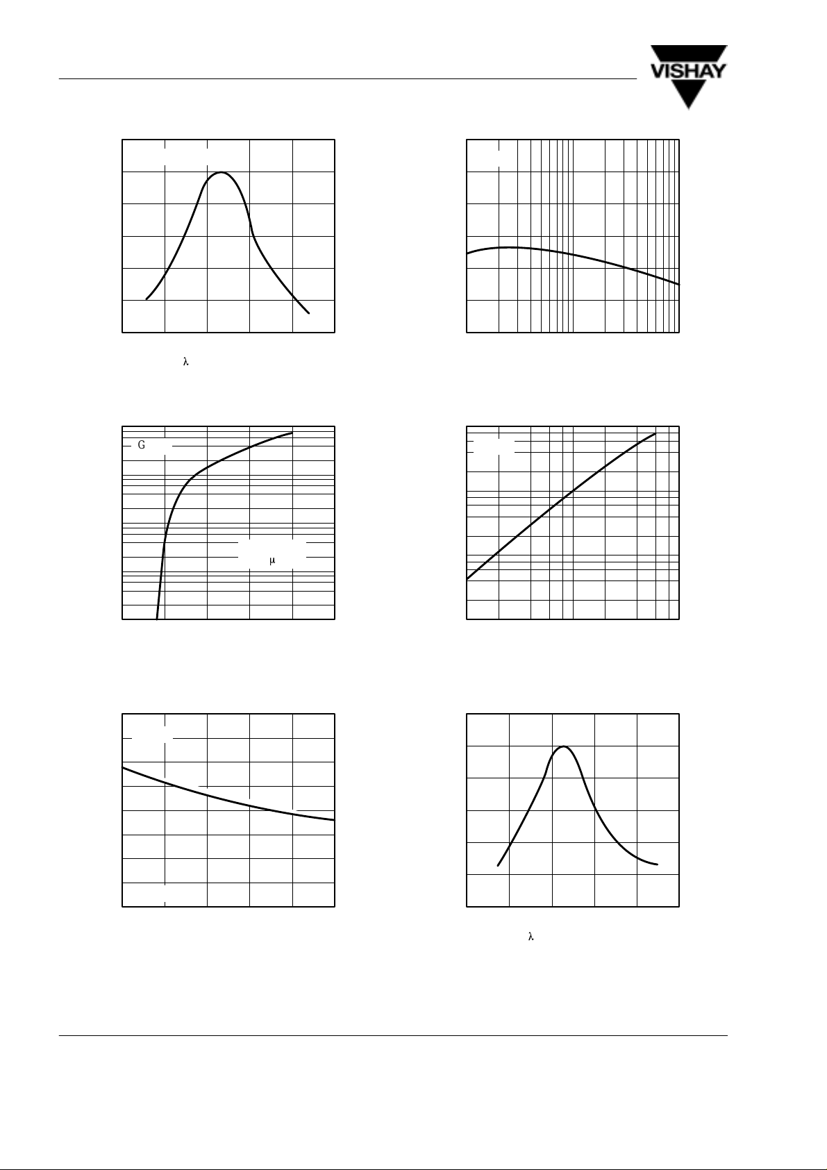
Figure 9 Relative Luminous Intensity vs. Wavelength
1000
Green
100
10
2.4
Green
2.0
1.6
1.2
0.8
0.4
v rel
I – Specific Luminous Intensity
0
10 20 50 100 200
95 10263
IF – Forward Current ( mA )
Figure 12 Specific Luminous Intensity vs.
Forward Current
10
Green
1
500
tp/T=0.001
=10ms
t
1
F
I – Forward Current ( mA )
p
0.1
02468
95 10034 V
– Forward Voltage ( V )
F
Figure 10 Forward Current vs. Forward Voltage
1.6
Green
1.2
0.8
0.4
v rel
I – Relative Luminous Intensity
95 10035
0
IF=10mA
0
20 40 60 80
T
– Ambient Temperature ( °C )
amb
Figure 11 Rel. Luminous Intensity vs.
Ambient Temperature
10
100
0.1
v rel
I – Relative Luminous Intensity
0.01
100
95 10037
110
I
– Forward Current ( mA )
F
Figure 13 Relative Luminous Intensity vs.
Forward Current
1.2
Green
1.0
0.8
0.6
0.4
0.2
v rel
I – Relative Luminous Intensity
0
620
95 10038
520 540 560 580 600
l
– Wavelength ( nm )
Figure 14 Relative Luminous Intensity vs. Wavelength
www.vishay .de • FaxBack +1-408-970-5600 Document Number 83052
4 (6)
Rev. A1, 04-Feb-99
Page 5
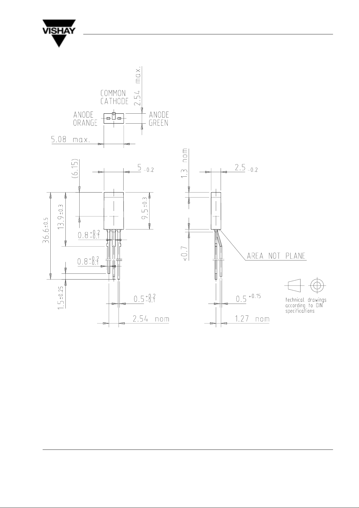
Dimensions in mm
TLSV5100
Vishay Telefunken
95 11327
Document Number 83052
Rev. A1, 04-Feb-99
www.vishay .de • FaxBack +1-408-970-5600
5 (6)
Page 6

TLSV5100
Vishay Telefunken
Ozone Depleting Substances Policy Statement
It is the policy of Vishay Semiconductor GmbH to
1. Meet all present and future national and international statutory requirements.
2. Regularly and continuously improve the performance of our products, processes, distribution and operating
systems with respect to their impact on the health and safety of our employees and the public, as well as their
impact on the environment.
It is particular concern to control or eliminate releases of those substances into the atmosphere which are known as
ozone depleting substances (ODSs).
The Montreal Protocol (1987) and its London Amendments (1990) intend to severely restrict the use of ODSs and
forbid their use within the next ten years. V arious national and international initiatives are pressing for an earlier ban
on these substances.
Vishay Semiconductor GmbH has been able to use its policy of continuous improvements to eliminate the use of
ODSs listed in the following documents.
1. Annex A, B and list of transitional substances of the Montreal Protocol and the London Amendments respectively
2. Class I and II ozone depleting substances in the Clean Air Act Amendments of 1990 by the Environmental
Protection Agency (EPA) in the USA
3. Council Decision 88/540/EEC and 91/690/EEC Annex A, B and C (transitional substances) respectively.
Vishay Semiconductor GmbH can certify that our semiconductors are not manufactured with ozone depleting
substances and do not contain such substances.
We reserve the right to make changes to improve technical design and may do so without further notice.
Parameters can vary in different applications. All operating parameters must be validated for each customer application
by the customer. Should the buyer use Vishay-Telefunken products for any unintended or unauthorized application, the
buyer shall indemnify Vishay-Telefunken against all claims, costs, damages, and expenses, arising out of, directly or
indirectly , any claim of personal damage, injury or death associated with such unintended or unauthorized use.
Vishay Semiconductor GmbH, P.O.B. 3535, D-74025 Heilbronn, Germany
Telephone: 49 (0)7131 67 2831, Fax number: 49 (0)7131 67 2423
www.vishay .de • FaxBack +1-408-970-5600 Document Number 83052
6 (6)
Rev. A1, 04-Feb-99
 Loading...