

Page 1
TLP721(D4,M)SERIES,TLP733(D4,M)SERIES,TLP747(D4,M)SERIES
TOSHIBA PHOTOCOUPLER
TLP721(D4,M)SERIES,TLP733(D4,M)SERIES,TLP747(D4,M)SERIES
ATTACHMENT
Types : TLP721, TLP721F, TLP733, TLP733F, TLP734, TLP734F, TLP747G, TLP747GF, TLP747J,
This data sheet refers to black mold-resin devices, TLPxxx (D4xxx, M) that previously has a white-resin mold
and have been changed. When designing new products please use black mold-resin devices.
Type designations for 'Option: (D4)
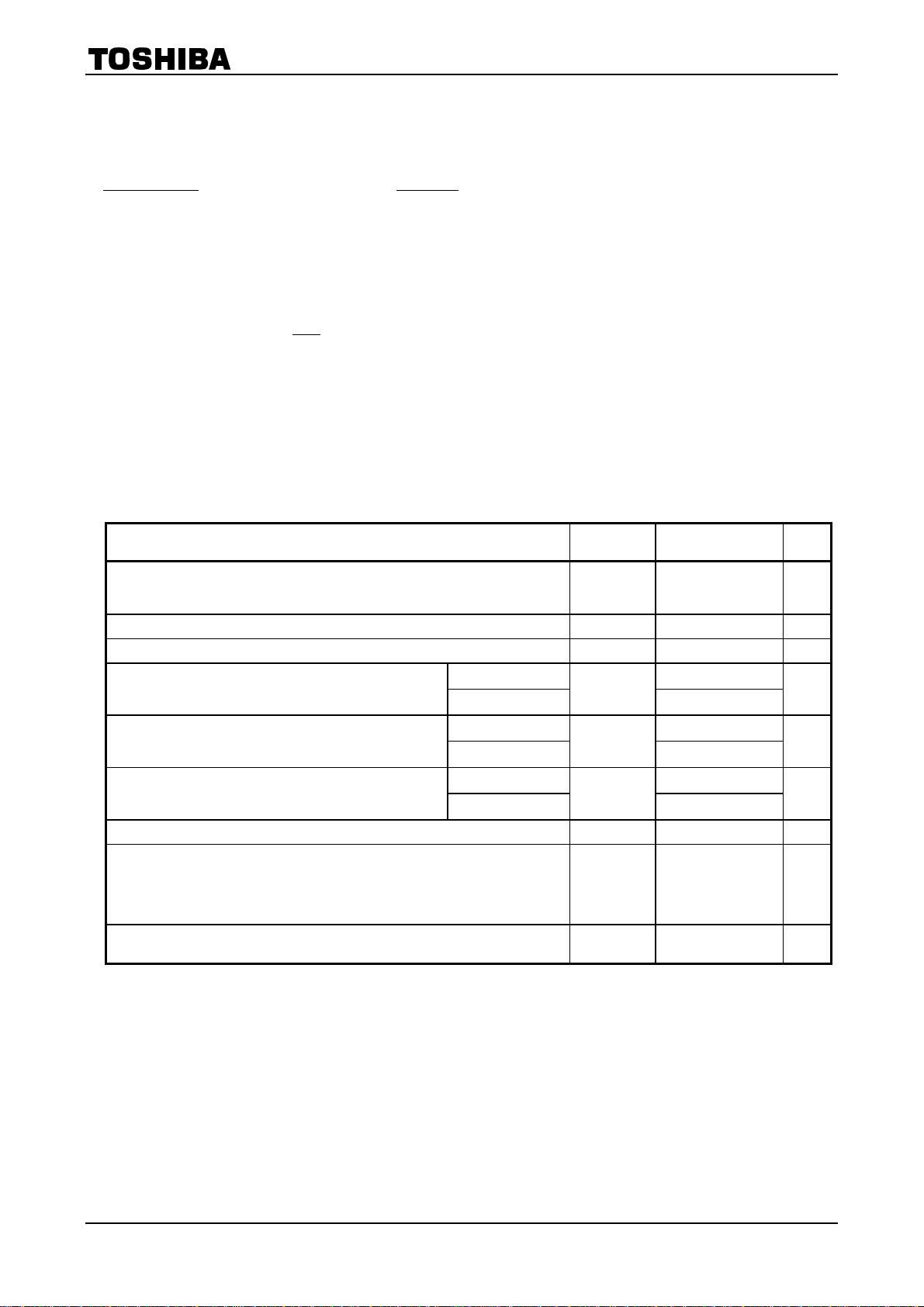
VDE0884 ISOLATION CHARACTERISTICS
: SPECIFICATIONS FOR VDE0884 OPTION: (D4)
TLP747JF
', which are tested under VDE0884 requirements.
Ex. : TLP734F (D4-GR-LF4, M) D4 : VDE0884 option
GR : CTR rank name
LF4 : standard lead bend name
M : black mold-resin devices
Note : Use Toshiba standard type number for safety standard application.
Ex. TLP734(FD4-GR-LF4, M) → TLP734F
DESCRIPTION SYMBOL RATING UNIT
Application Classification (DIN VDE0110 Teil 2 / 01.89, Table 1)
for rated mains voltage ≤ 300 V
for rated mains voltage ≤ 600 V
Climatic Classification (DIN IEC68 Teil 1 / 09.80) 40 / 100 / 21 ―
Pollution Degree (DIN VDE0110 Teil 2 / 01.89) 2 ―
Maximum Operating Insulation Voltage
Input to output Test Voltage, Method A
Vpr = 1.5 × V
tp = 60s, Partial Discharge < 5pC
Input to output Test Voltage, Method B
Vpr = 1.875 × V
tp = 1s, Partial Discharge < 5pC
Highest Permissible Overvoltage (Transient Overvoltage, tpr = 10s) VTR 8000 Vpk
Safety Limiting Values (Max. permissible ratings in case of fault, also refer to
thermal derating curve)
Current (Input current I
Power (Output or Total Powr Dissipation)
Temperature
Insulation Resistance, VIO = 500V, Ta = 25°C
, Type and Sample Test
IORM
, 100% Production Test
IORM
F
V
IO
RMS
RMS
, Psi = 0)
= 500V, Ta = Tsi
TLPxxx type 890
TLPxxxF type
TLPxxx type 1335
TLPxxxF type
TLPxxx type 1670
TLPxxxF type
V
IORM
Vpr
Vpr
Isi
Psi
Tsi
Rsi
I- IV
I- III
1130
1695
2120
400
700
150
≥10
≥109
12
―
Vpk
Vpk
Vpk
mA
mW
°C
Ω
1
2001-05-14
Page 2
TLP721(D4,M)SERIES,TLP733(D4,M)SERIES,TLP747(D4,M)SERIES
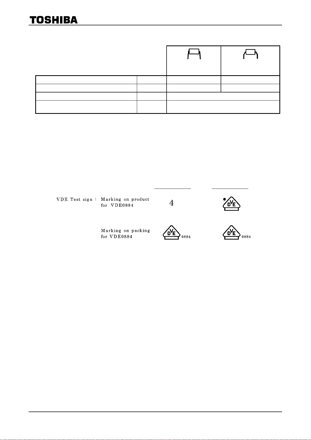
INSULATION RELATED SPECIFICATIONS
7.62mm pitch
TLPxxx type
Minimum Creepage Distance (*) Cr 7.0 mm 8.0 mm
Minimun Clearance (*) Cl 7.0 mm 8.0 mm
Minimum Insulation Thickness ti 0.5 mm
Comperative Tracking Index
(DIN IEC112 / VDE0303, Part 1)
*: in accordance with DIN VDE0110 Teil 1 / 01.89, Table 2, & 4
1. If a printed circuit is incorporated, the creepage distance and clearance may be reduced below this value
(e. g. at a standard distance between soldering eye centres of 7.5mm). If this is not permissible, the user
shall take suitable measures.
2. This photocoupler is suitable for 'safe electrical isolation' only within the safety limit data.
Maintenance of the safety data shall be ensured by means of protective circuits.
CTI
TLP721 SERIES
10.16mm pitch
TLPxxxF type
(VDE0110 Teil 2 / 01.89 Group IIIa)
175
TLP733 SERIES
TLP747 SERIES
2
2001-05-14
Page 3

TLP721(D4,M)SERIES,TLP733(D4,M)SERIES,TLP747(D4,M)SERIES
Figure 1 Partial discharge measurement procedure according to VDE0884
Destructive test for qualification and sampling tests.
Figure 2 Partial discharge measurement procedure according to VDE0884
Non-destructive test for 100% inspection.
Figure 3 Dependency of maximum safety ratings on ambient temperature
3
2001-05-14
Page 4

TLP721(D4,M)SERIES,TLP733(D4,M)SERIES,TLP747(D4,M)SERIES
RESTRICTIONS ON PRODUCT USE
· TOSHIBA is continually working to improve the quality and reliability of its products. Nevertheless, semiconductor
devices in general can malfunction or fail due to their inherent electrical sensitivity and vulnerability to physical
stress. It is the responsibility of the buyer, when utilizing TOSHIBA products, to comply with the standards of
safety in making a safe design for the entire system, and to avoid situations in which a malfunction or failure of
such TOSHIBA products could cause loss of human life, bodily injury or damage to property.
In developing your designs, please ensure that TOSHIBA products are used within specified operating ranges as
set forth in the most recent TOSHIBA products specifications. Also, please keep in mind the precautions and
conditions set forth in the “Handling Guide for Semiconductor Devices,” or “TOSHIBA Semiconductor Reliability
Handbook” etc..
· The TOSHIBA products listed in this document are intended for usage in general electronics applications
(computer, personal equipment, office equipment, measuring equipment, industrial robotics, domestic appliances,
etc.). These TOSHIBA products are neither intended nor warranted for usage in equipment that requires
extraordinarily high quality and/or reliability or a malfunction or failure of which may cause loss of human life or
bodily injury (“Unintended Usage”). Unintended Usage include atomic energy control instruments, airplane or
spaceship instruments, transportation instruments, traffic signal instruments, combustion control instruments,
medical instruments, all types of safety devices, etc.. Unintended Usage of TOSHIBA products listed in this
document shall be made at the customer’s own risk.
· Gallium arsenide (GaAs) is a substance used in the products described in this document. GaAs dust and fumes
are toxic. Do not break, cut or pulverize the product, or use chemicals to dissolve them. When disposing of the
products, follow the appropriate regulations. Do not dispose of the products with other industrial waste or with
domestic garbage.
· The products described in this document are subject to the foreign exchange and foreign trade laws.
000707EBC
· The information contained herein is presented only as a guide for the applications of our products. No
responsibility is assumed by TOSHIBA CORPORATION for any infringements of intellectual property or other
rights of the third parties which may result from its use. No license is granted by implication or otherwise under
any intellectual property or other rights of TOSHIBA CORPORATION or others.
· The information contained herein is subject to change without notice.
4
2001-05-14
 Loading...