

Datasheet TLP270M, TLP270G-1, TLP270G, TLP200M, TLP200G-1 Datasheet (SGS Thomson Microelectronics)
...Page 1
TLPxxM/G/G-1
ApplicationSpecific Discretes
A.S.D.
MAINAPPLICATIONS
Anysensitive telecomequipmentrequiringprotectionagainst lightning :
Analogand ISDN line cards
MainDistributionFrames
Terminaland transmissionequipment
Gas-tubereplacement
DESCRIPTION
The TLPxxM/G/G-1 series are tripolar transient
surge arrestors used for primary and secondary
protectionin sensitivetelecomequipment.
FEATURES
TRIPOLARCROWBAR PROTECTION
VOLTAGE RANGE SELECTED FOR
TELECOMAPPLICATIONS
PROTECTIONfor TELECOM LINE
TRIPOLAR OVERVOLTAGE
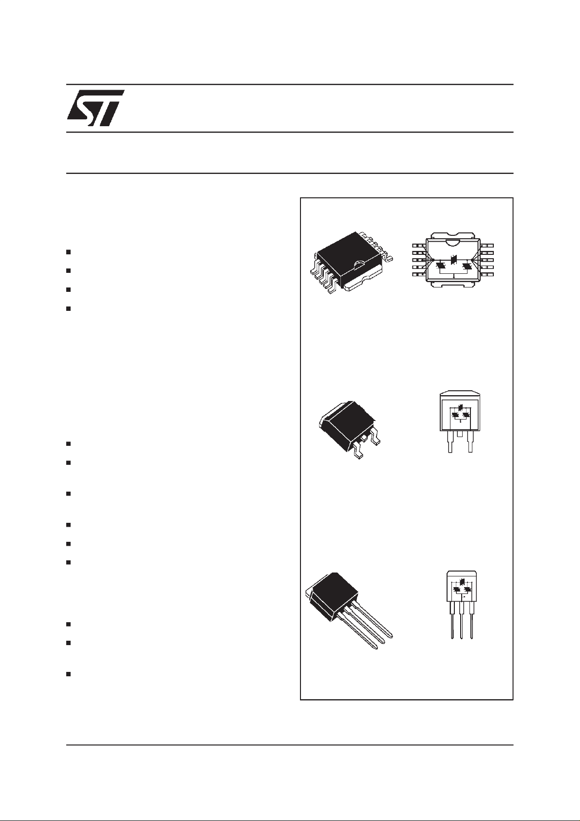
GND
TIP
PowerSO-10TMTLPxxM
GND
TAB
GND
D2PAK TLPxxG
RINGTIP
RINGTIP
RING
RINGTIP
RINGTIP
RINGTIP
REPETITIVEPEAK PULSE CURRENT:
= 100A (10/ 1000µs)
I
PP
HOLDINGCURRENT: I
= 150mA
H
LOWCAPACITANCE: C = 110 pF typ.
LOWLEAKAGECURRENT: I
=5µA max
R
BENEFITS
No ageing and no noise.
If destroyed, the TLPxxM/G/G-1 falls into short
circuit,still ensuringprotection.
Access to Surface Mount applications thanks to
TM
the PowerSO-10
TM: ASD and PowerSO-10 are trademarks of ST Microelectronics.
September 1998 - Ed : 3C
andD2PAKpackage.
2
I
PAK TLPxxG-1
GND
TAB
GND RINGTIP
1/14
Page 2
TLPxxM/G/G-1
COMPLIESWITH THE
FOLLOWINGSTANDARDS:
PeakSurge
Voltage
(V)
Voltage
Waveform
(µs)
Current
Waveform
(µs)
Admissible
Ipp
(A)
Necessary
Resistor
CCITTK20 4000 10/700 5/310 100 VDE0433
4000 10/700 5/310 100 VDE0878 4000 1.2/50 1/20 100 IEC-1000-4-5 level 4
level 4
FCC Part68, lightningsurge
type A
FCC Part68, lightningsurge
1500
800
1000 5/320 5/320 25 -
10/700
1.2/50
10/160
10/560
5/310
8/20
10/160
10/560
100
100
200
100
type B
BELLCORETR-NWT-001089
FIRSTLEVEL
BELLCORETR-NWT-001089
2500
1000
2/10
10/1000
2/10
10/1000
500
100
5000 2/10 2/10 500 SECONDLEVEL
CNETI31-24 4000 0.5/700 0.8/310 100 -
TYPICALAPPLICATION
Primaryprotection module
(Ω)
-
-
-
-
-
-
TLPxxM/G/G-1
Main Distribution Frame
Analog line card protection
LINE A
TLPxxM/G/G-1
PTC
RING
RELAY
LCP1511D
Analog
Line
Card
220
-Vbat
SLIC
nF
2/14
LINE B
PTC
Page 3
TYPICALAPPLICATION
ISDN: U interfaceprotection
TLPxxM/G/G-1
TLPxxM/G/G-1
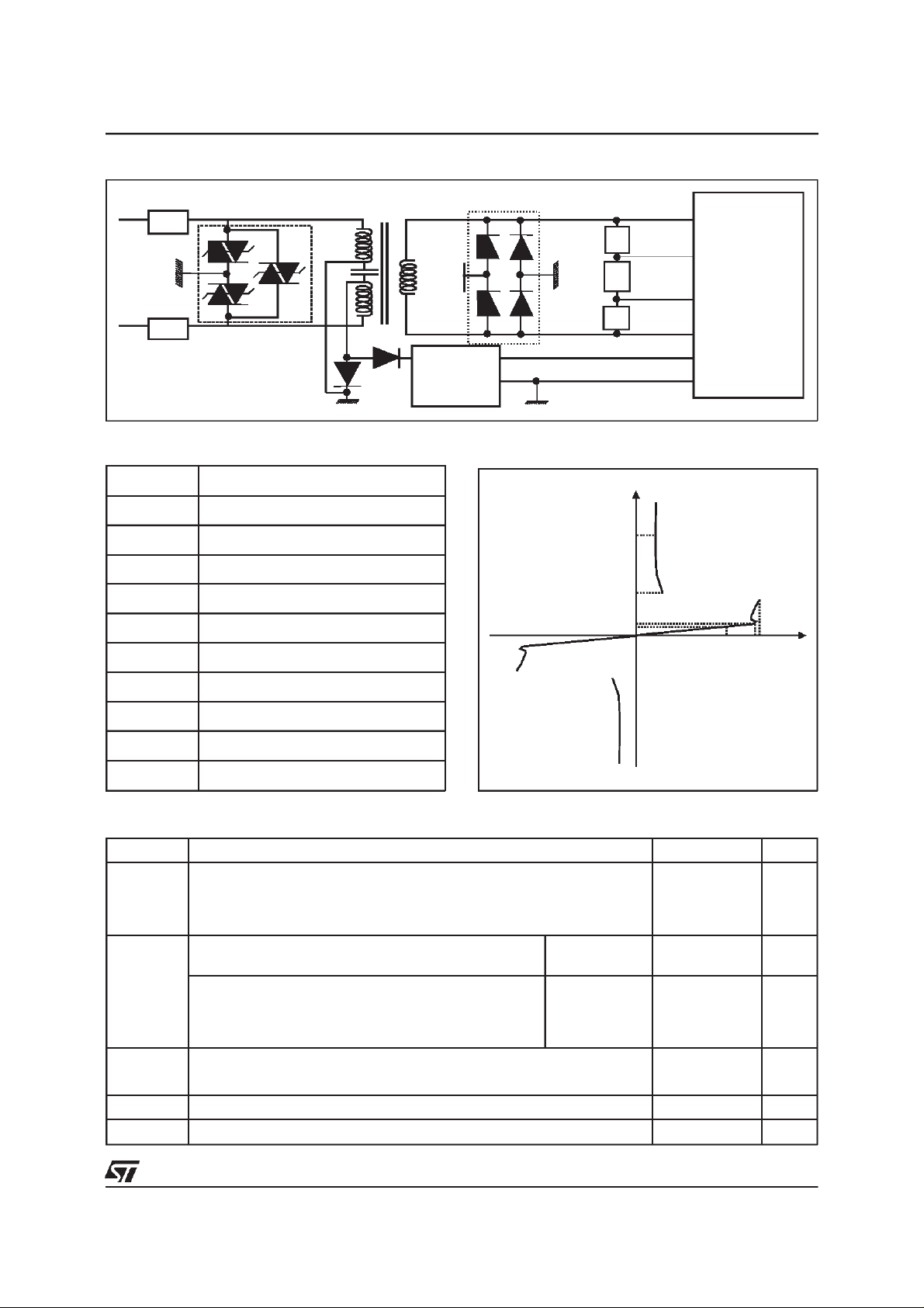
PARAMETER MEASUREMENT INFORMATION
Symbol Description
I
PP
I
TSM
I
I
RM
I
V
R
H
BR
Peak pulse current
Maximumpeak on-statecurrent
Leakagecurrent
Leakagecurrent
Holdingcurrent
Breakdownvoltage
1/2 DA108S1
+5V
Power
Feeder
R3
R4
R5
IRM
IPP
IR
Internal
circuitry
IH
VRM
VRVBO
V
R
V
RM
V
BO
Continuousreversevoltage
Maximumstand-off voltage
Breakovervoltage
C Capacitance
ABSOLUTE MAXIMUMRATINGS
(T
amb
=25°C)
Symbol Parameter Value Unit
I
PP
I
TSM
Peakpulse current(longitudinal& transversalmode) :
10/1000µs (opencircuitvoltagewaveform1 kV 10/1000µs)
8/20µs (opencircuit voltagewaveform4 kV 1.2/50µs)
2/10µs (opencircuit voltage waveform2.5kV 2/10 µs)
Mainspowerinduction
t = 200ms 0.7 A
100
250
500
VRMS= 300V,R = 600Ω
Mainspowercontact
V
= 220V,R =10Ω (Fail-Safethreshold) t = 200 ms
RMS
=220V, R = 600
V
RMS
T
stg
Storagetemperaturerange - 55 to+ 150 °C
Ω
t = 15 mn 0.42 A
31 A
Tj Maximumoperatingjunctiontemperature 150 °C
T
L
T
OP
Maximumleadtemperaturefor solderingduring10 s 260 °C
Operatingtemperaturerange - 40 to+ 85 °C
A
A
A
3/14
Page 4
TLPxxM/G/G-1
THERMALRESISTANCE
Symbol Parameter Value Unit
Rth (j-c) Junctionto case TLPxxM
TLPxxG
TLPxxG-1
Rth (j-a) Junctionto ambient TLPxxM
TLPxxG
TLPxxG-1
seetable page 14
seetable page 14
seetable page 14
1.0
1.0
1.0
C/W
°
°C/W
ELECTRICAL CHARACTERISTICS BETWEEN TIP AND RING
@V
I
Type
RM
max. max. typ.
RM
(T
amb
IR@V
=25°C)
R
note
µAVµAVpF
TLP140M/G/G-1
TLP200M/G/G-1
TLP270M/G/G-1
Note : VR= 50 V bias, V
= 1V, F = 1 MHz.
RMS
ELECTRICALCHARACTERISTICS BETWEEN TIP AND GND, RINGAND GND(T
I
RM
Type
max.
5 120 50 140 35
5 180 50 200 35
5 230 50 270 35
=25°C)
amb
@V
RM
IR@V
R
V
BO
I
BO
@
IH C @ V
max. max. max. min. typ.
note 1 note 2 note 3 note 4 note 5
µAVµAV VmAmApFpF
TLP140M/G/G-1
5 120 50 140 200 500 150 110 40
TLP200M/G/G-1 5 180 50 200 290 500 150 110 40
TLP270M/G/G-1
Note 1: IRmeasured at VRguaranteesV
Note 2: Measured at 50 Hz.
Note 3: See functional holdingcurrent test circuit.
Note 4: VR= 0V bias, V
Note 5: VR= 50V bias, V
5 230 50 270 400 500 150 110 40
BR min>VR
= 1V, F = 1 MHz.
RMS
= 1V, F = 1 MHz (TIPor RING (-) / GND (+)).
RMS
.
C
R
4/14
Page 5
FUNCTIONAL HOLDING CURRENT (IH) TEST CIRCUIT: GO-NO GOTEST
R
V
BAT
=
-48V
D.U.T .
TLPxxM/G/G-1
-V
P
Surge
generator
This is a GO-NOGO test which allowsto confirmthe holdingcurrent (IH)level in a functionaltest circuit.
TESTPROCEDURE:
- Adjust the currentlevelat theI
- FiretheD.U.T. with a surgecurrent: I
value by short circuitingthe D.U.T.
H
=10A, 10/1000µs.
PP
- The D.U.T.will come back to the off-statewithin a durationof 50ms max.
MARKING
Package Types Marking
PowerSO-10 TLP140M
TLP200M
TLP270M
2
PAK TLP140G
D
TLP200G
TLP270G
2
PAK TLP140G-1
I
TLP200G-1
TLP270G-1
TLP140M
TLP200M
TLP270M
TLP140G
TLP200G
TLP270G
TLP140G
TLP200G
TLP270G
ORDERCODE
TripolarLine Protection
TPL 270 M-TR
BreakdownVoltage
Packaging:
-TR=tapeandreelonlyfor”M”versi on(600pcs)
= tube(50 pcs)
Package:
M: PowerSO10
2
PAK
G:D
2
G-1: I
PAK
5/14
Page 6

TLPxxM/G/G-1
Fig.1: Maximum peak on-statecurrent versus
pulseduration.
ITSM(A)
100
90
80
70
60
50
40
30
20
10
0
0.01 0.1 1 10 100 1000
TIP or RING
vs GND
t(s)
F=50Hz
Tj initial=25°C
Fig.3-1 :junction capacitanceversus applied reversevoltage(typical values)(TLP140M/G/G-1).
C(pF)
200
100
50
LINE+ /GND-
LINE / LINE
LINE- / GND+
F=1MHz
Vosc=1VRMS
Tj=25°C
Fig.2: Relativevariation of IHversusT
IH (Tamb) / IH (25°C)
2
1.8
1.6
1.4
1.2
1
0.8
0.6
0.4
-40-200 20406080
Fig.3-2 :
junctioncapacitanceversus appliedre-
Tamb(°C)
amb
.
versevoltage(typical values)(TLP200M/G/G-1).
C(pF)
200
100
50
LINE+ / GND-
LINE / LINE
LINE- /GND+
F=1MHz
Vosc=1VRMS
Tj=25°C
20
VR(V)
10
1 10 100 200
Fig.3-3 :junction capacitanceversus applied reversevoltage(typical values)(TLP270M/G/G-1).
C(pF)
200
100
50
LINE / LINE
LINE- / GND+
LINE+ / GND-
20
VR(V)
10
1 10 100 300
F=1MHz
Vosc=1VRMS
Tj=25°C
20
VR(V)
10
1 10 100 200
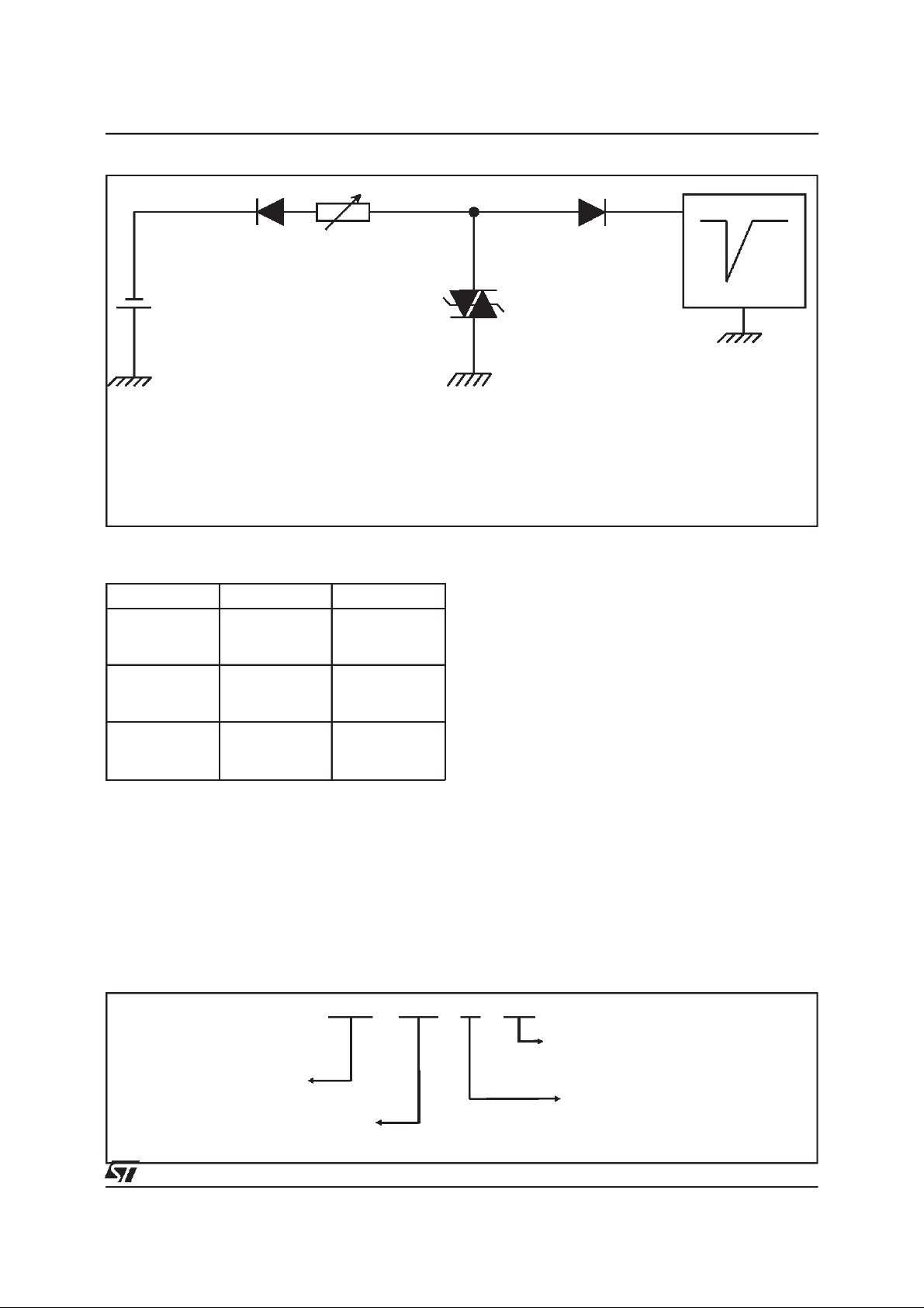
Fig.4: Test diagram for breakover voltage
measurement.
TIP
10 / 1000 µs
100 A
surgegenerator
BO
V
TIP RING
GND
RING
V
BO
TIP - GND
6/14
Page 7

TLPxxM/G/G-1
Fig.5-1 : Breakovervoltagemeasurement
(TLP140M/G/G-1).
Vbr/Vbr
2.6
2.4
2.2
2
1.8
1.6
1.4
1.2
1
0.01 0.1 1 10 100 1,000 10,000 100,000
TIP RING
TIP+ GND -
TIP- GND +
dV/dt
Fig.5-3 : Breakovervoltagemeasurement
(TLP270M/G/G-1).
Vbo/Vbr
2.6
2.4
2.2
2
1.8
1.6
1.4
1.2
1
0.01 0.1 1 10 100 1,000 10,000 100,000
TIP RING
TIP+ GND -
TIP- GND +
dV/dt
Fig. 5-2 :
Breakovervoltage measurement
(TLP200M/G/G-1).
Vbo/Vbr
2.6
2.4
2.2
2
1.8
1.6
1.4
1.2
1
0.01 0.1 1 10 100 1,000 10,000 100,000
TIP RING
TIP+ GND -
TIP- GND +
dV/dt
7/14
Page 8

TLPxxM/G/G-1
PACKAGEMECHANICAL DATA
2
D
PAK Plastic
E
L2
L
L3
A1
B2
B
G
2.0 MIN.
FLAT ZONE
C2
DIMENSIONS
A
REF.
Millimeters Inches
Min. Typ. Max. Min. Typ. Max.
A 4.30 4.60 0.169 0.181
A1 2.49 2.69 0.098 0.106
A2 0.03 0.23 0.001 0.009
D
B 0.70 0.93 0.027 0.037
B2 1.40 0.055
C 0.45 0.60 0.017 0.024
C2 1.21 1.36 0.047 0.054
C
R
D 8.95 9.35 0.352 0.368
E 10.00 10.28 0.393 0.405
G 4.88 5.28 0.192 0.208
L 15.00 15.85 0.590 0.624
A2
L2 1.27 1.40 0.050 0.055
L3 1.40 1.75 0.055 0.069
R 0.40 0.016
V2
V2 0° 8° 0° 8°
FOOT-PRINT D
10.30
2
PAK
8.90
16.90
5.08
1.30
3.70
8/14
Page 9

PACKAGEMECHANICAL DATA
2
PAK Plastic
I
TLPxxM/G/G-1
DIMENSIONS
REF.
A 4.30 4.60 0.169 0.181
A1 2.49 2.69 0.098 0.106
B 0.70 0.93 0.028 0.037
B1 1.20 1.38 0.047 0.054
B2 1.25 1.40 0.049 0.055
C 0.45 0.60 0.018 0.024
C2 1.21 1.36 0.048 0.054
D 8.95 9.35 0.352 0.368
e 2.44 2.64 0.096 0.104
E 10.00 10.28 0.394 0.405
L 13.10 13.60 0.516 0.535
L1 3.48 3.78 0.137 0.149
L2 1.27 1.40 0.050 0.055
V5° 5°
V4 45° 45°
Millimeters Inches
Min. Typ. Max. Min. Typ. Max.
9/14
Page 10

TLPxxM/G/G-1
PACKAGEMECHANICALDATA
Power-SO10
10
B
0.10 A B
6
H
A1
E
1
eB
E2
5
DETAIL ”A”
E3 E1
SEATING
PLANE
A
C
0.25 M
D
h
D1
Q
A
F
SEATING
PLANE
A1
L
DETAIL”A”
E4
a
DIMENSIONS
REF.
Millimeters Inches
Min. Typ. Max. Min. Typ. Max.
A 3.35 3.65 0.131 0.143
A1 0.00 0.10 0.00 0.0039
B 0.40 0.60 0.0157 0.0236
C 0.35 0.55 0.0137 0.0217
D 9.40 9.60 0.370 0.378
D1 7.40 7.60 0.291 0.299
E 9.30 9.50 0.366 0.374
E1 7.20 7.40 0.283 0.291
E2 7.20 7.60 0.283 0.299
10/14
DIMENSIONS
REF.
Millimeters Inches
Min. Typ. Max. Min. Typ. Max.
E3 6.10 6.35 0.240 0.250
E4 5.90 6.10 0.232 0.240
e 1.27 0.05
F 1.25 1.35 0.0492 0.0531
H 13.80 14.40 0.543 0.567
h 0.50 0.019
L 1.20 1.80 0.0472 0.0708
Q 1.70 0.067
a0° 8°0° 8°
Page 11

TLPxxM/G/G-1
FOOTPRINT
MOUNTINGPADLAYOUT
RECOMMENDED
Dimensionsin millimeters Dimensionsin millimeters
SHIPPINGTUBE
Power-SO10
HEADERSHAPE
C
B
A
Surfacemountfilm taping: contactsales office
A
B
C
Lengthtube
Quantityper tube
DIMENSIONS(mm)
TYP
18
12
0,8
532
50
11/14
Page 12

TLPxxM/G/G-1
SOLDERINGRECOMMENDATION
The soldering process causes considerable thermal stress to a semiconductor component. This
has to be minimized to assure a reliable and extended lifetime of the device. The PowerSO-10
package can be exposed to a maximumtemperature of 260°Cfor 10 seconds. However a proper
soldering of the package could be done at 215°C
for 3 seconds. Any solder temperature profile
shouldbe withinthese limits. As reflow techniques
are most common in surface mounting, typical
heating profiles are given in Figure 1,either for
mountingon FR4 or on metal-backed boards. For
each particular board, the appropriate heat profile
has to be adjusted experimentally. The present
proposalisjusta startingpoint. Inanycase,the followingprecautions haveto be considered:
- alwayspreheatthe device
- peaktemperatureshould be at least30 °C
higherthan the melting point of the solder
alloychosen
- thermalcapacityof the base substrate
Fig. 1 : Typicalreflow solderingheat profile
Voids pose a difficult reliability problem for large
surface mount devices. Such voids under the
package result in poor thermal contact and the
high thermal resistance leads to component failures.The PowerSO-10is designedfromscratchto
besolelya surfacemountpackage,hencesymmetry inthe x-and y-axis givesthe packageexcellent
weightbalance.Moreover, the PowerSO-10offers
the unique possibilityto control easily the flatness
and quality of the soldering process. Both the top
and the bottom soldered edgesof thepackageare
accessible for visual inspection (soldering meniscus).
Coplanarity between the substrate and the package canbe easilyverified.The qualityof the solder
joints is very important for two reasons : (I) poor
qualitysolder joints result directlyin poor reliability
and (II) solder thickness affects the thermal resistance significantly.Thus a tight control of this parameter results in thermally efficient and reliable
solderjoints.
Temperature ( C)
250
o
o
245 C
o
215 C
200
Soldering
Cooli ng
150
Epoxy FR4
board
Preheating
100
Metal-backed
50
board
0
0 40 80 120 160 200 2 40 280 320 360
Time (s)
12/14
Page 13

TLPxxM/G/G-1
SUBSTRATES AND MOUNTINGINFORMATION
The use of epoxy FR4 boards is quite commonfor
surface mounting techniques, however, their poor
thermal conductioncompromisesthe otherwise
outstandingthermalperformanceof thePowerSO-
10. Some methodsto overcome this limitation are
discussedbelow.
One possibility to improve the thermal conduction
is the use of large heat spreader areas at the copper layerofthe PC board.Thisleadsto areduction
of thermal resistance to 35 °C for 6 cm
2
of the
board heatsink(seefig. 2).
Use of copper-filledthrough holes on conventional
FR4 techniqueswill increase the metallizationand
Fig.2 :
Mountingon epoxy FR4 head dissipationby extendingthe area of the copper layer
Copper foil
decrease thermal resistance accordingly. Using
a configurationwith 16holesunderthe spreaderof
the package with a pitchof 1.8 mm and a diameter
of 0.7 mm, the thermal resistance (junction heatsink) can be reduced to 12°C/W(see fig. 3).
Besidethe thermal advantage, thissolutionallows
multi-layer boards to be used. However, a drawback of this traditional material prevents its use in
veryhighpower,highcurrentcircuits.Forinstance,
it is not advisable to surface mount devices with
currents greater than 10 A on FR4 boards. A
PowerMosfetorSchottkydiodein a surfacemount
power package can handle up to around 50 A if
bettersubstratesare used.
FR4 board
Fig. 3 :
Mountingon epoxy FR4 by using copper-filledthroughholesfor heattransfer
Copperfoil
heattransferheatsink
FR4board
13/14
Page 14

TLPxxM/G/G-1
A new technologyavailable today is IMS - anInsulated Metallic Substrate. This offers greatly enhanced thermal characteristics for surface
mount components. IMS is a substrateconsisting
of threedifferentlayers,(I)thebasematerialwhich
is available as an aluminiumor a copper plate, (II)
a thermal conductive dielectrical layer and (III) a
copper foil, which can be etched as a circuitlayer.
Using this material a thermal resistanceof 8°C/W
with 40 cm
2
of board floating in air is achievable
(seefig. 4).If evenhigherpower isto be dissipated
an externalheatsink could be appliedwhich leads
to an R
that R
(j-a) of 3.5°C/W (see Fig. 5), assuming
th
(heatsink-air) is equal to Rth(junction-
th
heatsink). This is commonly applied in practice,
leading to reasonable heatsink dimensions. Often
power devices are defined by considering the
maximum junction temperature of the device. In
practice, however, this is far from being exploited.
A summary of various power management capabilities is made in table 1 based on a reasonable
deltaT of 70°Cjunctionto air.
The PowerSO-1 0 concept also represents an
attractive alternative to C.O.B. techniques.
PowerSO-10 offers devices fully tested at low
and high temperature. Mounting is simple - only
conventionalSMT is required - enabling the users
togetrid ofbondwire problemsandtheproblem to
controlthe high temperaturesoft solderingas well.
An optimized thermal management is guaranteed
through PowerSO-10 as the power chips must in
any case be mounted on heat spreaders before
beingmountedonto the substrate.
Fig. 4 : Mountingon metalbacked board Fig. 5 :
externalheatsinkapplied
Copperfoil
Copper foil
Alumini um
Insulation
Mountingon metal backed board with an
FR4board
Aluminium
heatsink
TABLE1
Printedcircuit board material Rth(j-a) P Diss
1.FR4using the recommended pad-layout 50°C/W 1.5W
2
2.FR4with heatsinkon board(6cm
3.FR4with copper-filledthrough holes and externalheatsinkapplied
2
4.IMSfloatingin air(40 cm
)8°C/W 8.8 W
)35°C/W 2.0 W
12°C/W 5.8W
5.IMSwith externalheatsink applied 3.5°C/W 20W
Informationfurnished isbelievedto be accurate and reliable. However, STMicroelectronics assumes no responsibility for the consequences of
use of such informationnor forany infringementof patents or other rights of thirdparties which mayresult from its use. Nolicense is granted by
implication or otherwise under any patent or patent rights of STMicroelectronics. Specifications mentioned in this publication are subject to
change without notice. This publication supersedes and replaces all information previously supplied.
STMicroelectronics products are not authorized for use as critical components in life support devices or systems withoutexpress written approval of STMicroelectronics.
The ST logo is a registeredtrademark of STMicroelectronics
1998STMicroelectronics - Printed in Italy - All rights reserved.
STMicroelectronics GROUP OF COMPANIES
Australia - Brazil - Canada - China - France - Germany - Italy - Japan - Korea -Malaysia - Malta - Mexico - Morocco -
The Netherlands - Singapore - Spain - Sweden - Switzerland - Taiwan - Thailand -United Kingdom - U.S.A.
http://www.st.com
14/14
 Loading...