

Page 1
TLC7225C, TLC7225I
QUADRUPLE 8-BIT DIGITAL-TO-ANALOG CONVERTERS
SLAS109A – OCTOBER 1996 – REVISED APRIL 1997
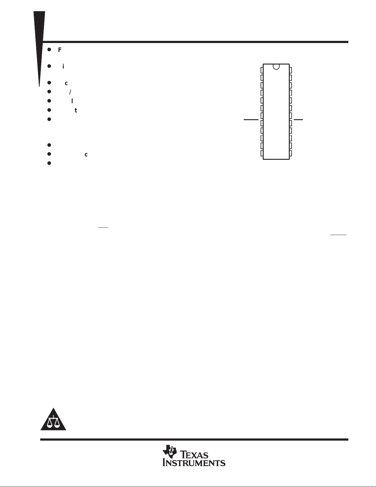
OUTB
OUTA
V
SS
REFB
REFA
AGND
DGND
LDAC
DB6
DB5
DB4
DW PACKAGE
(TOP VIEW)
1
24
2
23
3
22
4
21
5
20
6
19
7
18
8
17
9
16
10
15
11
14
12
13
OUTC
OUTD
V
DD
REFC
REFD
A0
A1
WR
DB0 (LSB)
DB1
DB2
DB3
D
Four 8-Bit D/A Converters With Individual
References
D
Direct Bipolar Operation Without an
External Level-Shift Amplifier
D
Microprocessor Compatible
D
TTL/CMOS Compatible
D
Single Supply Operation Possible
D
Simultaneous Update Facility
D
Binary Input Coding
applications
D
Process Control
D
Automatic Test Equipment
D
Automatic Calibration of Large System
Parameters e.g., Gain/Offset
(MSB) DB7
description
The TLC7225 consists of four 8-bit voltage-output digital-to-analog converters (DACs), with output buffer
amplifiers and interface logic with double register-buffering.
Separate on-chip latches are provided for each of the DACs. Data is transferred into one of these data latches
through a common 8-bit TTL/CMOS-compatible (5 V) input port. Control inputs A0 and A1 determine which DAC
is loaded when WR
converters. The double register buffering allows simultaneous update of all four outputs under control of LDAC
All logic inputs are TTL- and CMOS-level compatible and the control logic is speed compatible with most 8-bit
microprocessors. Each DAC includes an output buffer amplifier capable of driving up to 5 mA of output current.
goes low. Only the data held in the DAC registers determines the analog outputs of the
.
The TLC7225 performance is specified for input reference voltages from 2 V to V
– 4 V with dual supplies.
DD
The voltage-mode configuration of the DACs allow the TLC7225 to be operated from a single power-supply rail
at a reference of 10 V.
The TLC7225 is fabricated in a LinBiCMOS process that has been specifically developed to allow high-speed
digital logic circuits and precision analog circuits to be integrated on the same chip. The TLC7225 has a common
8-bit data bus with individual DAC latches. This provides a versatile control architecture for simple interface to
microprocessors. All latch-enable signals are level triggered.
Combining four DACs, four operational amplifiers, and interface logic into a small, 0.3-inch wide, 24-terminal
SOIC allows significant reduction in board space requirements and offers increased reliability in systems using
multiple converters. The pinout optimizes board layout with all of the analog inputs and outputs at one end of
the package and all of the digital inputs at the other.
The TLC7225C is characterized for operation from 0°C to 70°C. The TLC7225I is characterized for operation
from –40°C to 85°C.
Please be aware that an important notice concerning availability, standard warranty, and use in critical applications of
Texas Instruments semiconductor products and disclaimers thereto appears at the end of this data sheet.
LinBiCMOS is a trademark of Texas Instruments Incorporated.
PRODUCTION DATA information is current as of publication date.
Products conform to specifications per the terms of Texas Instruments
standard warranty. Production processing does not necessarily include
testing of all parameters.
Copyright 1997, Texas Instruments Incorporated
POST OFFICE BOX 655303 • DALLAS, TEXAS 75265
1
Page 2
TLC7225C, TLC7225I
QUADRUPLE 8-BIT DIGITAL-TO-ANALOG CONVERTERS
SLAS109A – OCTOBER 1996 – REVISED APRIL 1997
AVAILABLE OPTIONS
PACKAGED DEVICES
SMALL OUTLINE
(DW)
DAC
Latch
A
DAC
Latch
B
DAC
Latch
C
DAC
Latch
D
DAC
DAC
DAC
DAC
A
B
C
D
functional block diagram
5
REFA
4
REFB
REFC
REFD
LDAC
WR
A0
A1
9–16
21
20
8
17
19
18
DB0–DB7
8
Control
Logic
T
A
0°C to 70°C TLC7225CDW
–40°C to 85°C TLC7225IDW
Input
8
Latch
A
Input
8
Latch
B
Input
8
Latch
C
Input
8
Latch
D
_
+
_
+
_
+
_
+
24
23
2
1
OUTA
OUTB
OUTC
OUTD
schematic of outputs
EQUIVALENT ANALOG OUTPUT
V
DD
100 µA
V
SS
Output
450 µA
2
POST OFFICE BOX 655303 • DALLAS, TEXAS 75265
Page 3
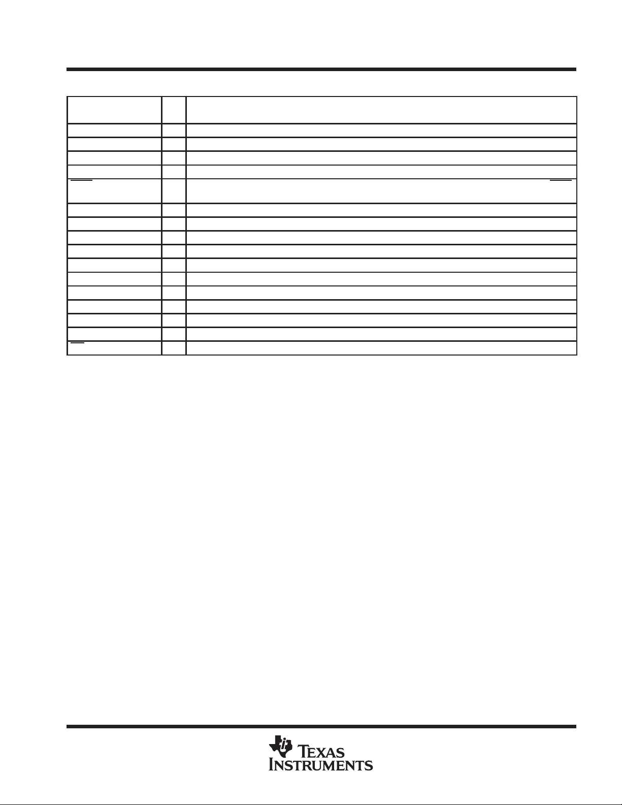
I/O
DESCRIPTION
TLC7225C, TLC7225I
QUADRUPLE 8-BIT DIGITAL-TO-ANALOG CONVERTERS
SLAS109A – OCTOBER 1996 – REVISED APRIL 1997
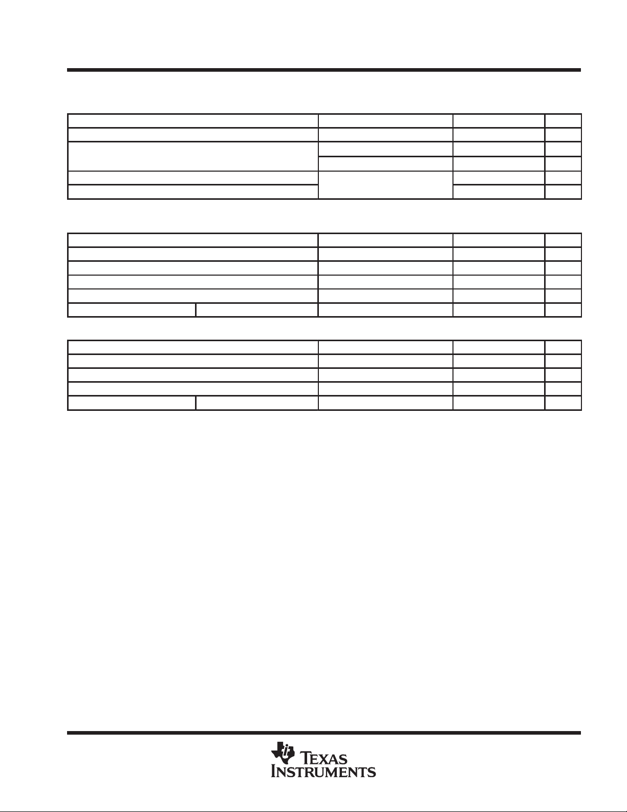
Terminal Functions
TERMINAL
NAME NO.
AGND 6 Analog ground
A0, A1 18, 19 I DAC select inputs
DGND 7 Digital ground
DB0 – DB7 9 – 16 I Digital DAC data inputs
LDAC 8 Load DAC. A high level simultaneously loads all four DAC registers. DAC registers are transparent when LDAC
is low.
OUTA 2 O DACA output
OUTB 1 O DACB output
OUTC 24 O DACC output
OUTD 23 O DACD output
REFA 5 I Voltage reference input to DACA
REFB 4 I Voltage reference input to DACB
REFC 21 I V oltage reference input to DACC
REFD 20 I V oltage reference input to DACD
V
DD
V
SS
WR 17 I Write input selects DAC transparency or latch mode
22 Positive supply voltage
3 Negative supply voltage
absolute maximum ratings over operating free-air temperature range (unless otherwise note)
Supply voltage range, V
Supply voltage range, V
Voltage range between AGND and DGND –0.3 V to V
Input voltage range, V
Reference voltage range, V
Output voltage range, V
Continuous total power dissipation at (or below) T
: to AGND or DGND –0.3 V to 17 V. . . . . . . . . . . . . . . . . . . . . . . . . . . . . . . . . . . . . . .
DD
to V
–0.3 V to 24 V. . . . . . . . . . . . . . . . . . . . . . . . . . . . . . . . . . . . . . . . . . . . . . . . . .
SS
: to AGND or DGND –7 V to V
SS
. . . . . . . . . . . . . . . . . . . . . . . . . . . . . . . . . . . . . . . . .
. . . . . . . . . . . . . . . . . . . . . . . . . . . . . . . . . . . . . . . . . . .
(to DGND) –0.3 V to VDD + 0.3 V. . . . . . . . . . . . . . . . . . . . . . . . . . . . . . . . . . . . . . . . . . . .
I
(to AGND) –0.3 V to V
ref
(to AGND) (see Note 1) VSS to V
O
. . . . . . . . . . . . . . . . . . . . . . . . . . . . . . . . . . . . . . . . . . . .
. . . . . . . . . . . . . . . . . . . . . . . . . . . . . . . . . . . . . . . .
= 25°C (see Note 2) 500 mW. . . . . . . . . . . . . . . . . . . . . . .
A
†
DD
DD
DD
DD
Operating free-air temperature range: C suffix 0°C to 70°C. . . . . . . . . . . . . . . . . . . . . . . . . . . . . . . . . . . . . . . . .
I suffix –40°C to 85°C. . . . . . . . . . . . . . . . . . . . . . . . . . . . . . . . . . . . . . . .
Storage temperature range, T
–65°C to 150°C. . . . . . . . . . . . . . . . . . . . . . . . . . . . . . . . . . . . . . . . . . . . . . . . . . .
stg
Lead temperature 1,6 mm (1/16 inch) from case for 10 seconds 260°C. . . . . . . . . . . . . . . . . . . . . . . . . . . . . . .
†
Stresses beyond those listed under “absolute maximum ratings” may cause permanent damage to the device. These are stress ratings only, and
functional operation of the device at these or any other conditions beyond those indicated under “recommended operating conditions” is not
implied. Exposure to absolute-maximum-rated conditions for extended periods may affect device reliability.
NOTES: 1. Output voltages may be shorted to AGND provided that the power dissipation of the package is not exceeded. Typically sh ort circuit
current to AGND is 50 mA.
2. For operation above TA = 75°C derate linearly at the rate of 2.0 mW/°C.
POST OFFICE BOX 655303 • DALLAS, TEXAS 75265
3
Page 4
TLC7225C, TLC7225I
Operating free-air temperature, T
QUADRUPLE 8-BIT DIGITAL-TO-ANALOG CONVERTERS
SLAS109A – OCTOBER 1996 – REVISED APRIL 1997
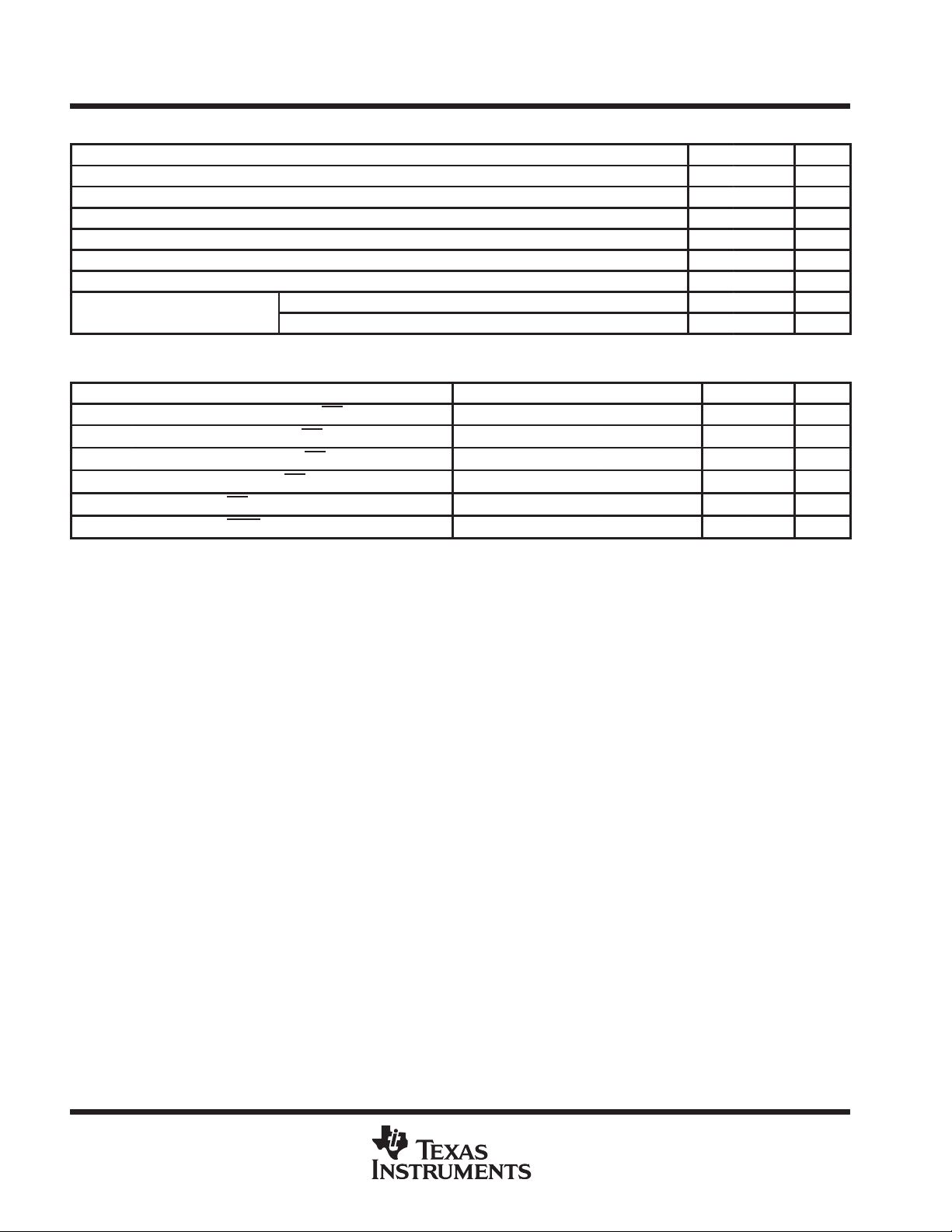
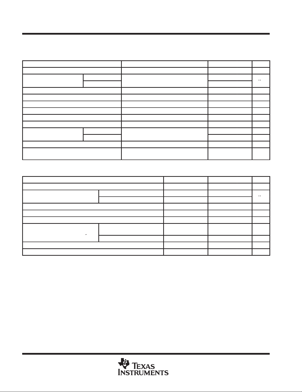
recommended operating conditions
Supply voltage, V
Supply voltage, V
High-level input voltage, V
Low-level input voltage, V
Reference voltage, V
Load resistance, R
p
timing requirements (see Figure 1)
t
su(AW)
t
su(DW)
t
h(AW)
t
h(DW)
t
w1
t
w2
DD
SS
IH
IL
ref
L
p
PARAMETER TEST CONDITIONS MIN MAX UNIT
Setup time, address valid before WR↓ 0 ns
Setup time, data valid before WR↑
Hold time, address valid after WR↑
Hold time, data valid after WR↑
Pulse duration, WR low
Pulse duration, LDAC low
C suffix 0 70 °C
A
I suffix –40 85 °C
VDD = 11.4 V to 16.5 V, VSS = 0 or –5 V 45 ns
VDD = 11.4 V to 16.5 V, VSS = 0 or –5 V 0 ns
VDD = 11.4 V to 16.5 V, VSS = 0 or –5 V 10 ns
VDD = 11.4 V to 16.5 V, VSS = 0 or –5 V 50 ns
VDD = 11.4 V to 16.5 V, VSS = 0 or –5 V 50 ns
MIN MAX UNIT
11.4 16.5 V
–5.5 0 V
2 V
0.8 V
2 VDD–4 V
2 kΩ
4
POST OFFICE BOX 655303 • DALLAS, TEXAS 75265
Page 5
CiIn ut ca acitance, REFA, REFB, REFC, REFD
V
10 V
sine wave at 10 kH
TLC7225C, TLC7225I
QUADRUPLE 8-BIT DIGITAL-TO-ANALOG CONVERTERS
SLAS109A – OCTOBER 1996 – REVISED APRIL 1997
electrical characteristics over recommended operating free-air temperature range
reference inputs (all supply ranges)
PARAMETER TEST CONDITIONS MIN TYP MAX UNIT
r
i
dual power supply over recommended supply and reference voltage ranges, AGND = DGND = 0 V (unless
otherwise noted)
I
I
I
DD
I
SS
C
i
Input resistance, REFA, REFB, REFC, REFD 1.5 4 kΩ
p
p
Channel-to-channel isolation
ac feedthrough
PARAMETER TEST CONDITIONS MIN TYP MAX UNIT
Input current, digital VI = 0 or V
Supply current, V
Supply current, V
Power supply sensitivity ∆VDD = ±5% 0.01 %/%
Input capacitance Digital inputs 8 pF
DD
SS
DAC loaded with all 1s 300 pF
DAC loaded with all 0s 65 pF
60 dB
=
ref
VI = VIL or VIH, No load 10 16 mA
VI = VIL or VIH, No load 4 10 mA
pp
DD
z
70 dB
±1 µA
single power supply, VDD = 14.25 V to 15.75 V, VSS = AGND = DGND = 0 V, V
PARAMETER TEST CONDITIONS MIN TYP MAX UNIT
I
I
C
I
DD
i
Input current, digital VI = 0 or V
Supply current, V
Power supply sensitivity ∆VDD = ±5% 0.01 %/%
Input capacitance Digital inputs 8 pF
DD
VI = VIL or VIH, No load 5 13 mA
DD
(A, B, C, D) = 10 V
ref
±1 µA
POST OFFICE BOX 655303 • DALLAS, TEXAS 75265
5
Page 6
TLC7225C, TLC7225I
tsSettling time to 1/2 LSB
V
10 V
s
V
V
V
tsSettling time to 1/2 LSB
s
g
QUADRUPLE 8-BIT DIGITAL-TO-ANALOG CONVERTERS
SLAS109A – OCTOBER 1996 – REVISED APRIL 1997
operating characteristics over recommended operating free-air temperature range
dual power supply over recommended supply and reference voltage ranges, AGND = DGND = 0 V (unless
otherwise noted)
PARAMETER TEST CONDITIONS MIN TYP MAX UNIT
Slew rate 2.5 V/µs
Positive full scale
Negative full scale
Resolution 8 Bits
Total unadjusted error VDD = 15 V ±5%, V
Integral nonlinearity (INL) VDD = 15 V ±5%, V
Differential nonlinearity (DNL) VDD = 15 V ±5%, V
E
E
Full-scale error VDD = 15 V ±5%, V
FS
Gain error VDD = 15 V ±5%, V
G
Temperature coefficient
of gain
Zero-code error ±20 ±80 mV
Digital crosstalk or feedthrough glitch
impulse area
Full-scale error
Zero-code error
ref(A, B, C, D)
= 14 V to 16.5 V,
DD
V
ref(A, B, C, D)
=
ref(A, B, C, D)
ref(A, B, C, D)
ref(A, B, C, D)
ref(A, B, C, D)
ref(A, B, C, D)
ref(A, B, C, D)
= 0 50 nV–s
= 10 V ±2 LSB
= 10 V ±1 LSB
= 10 V ±1 LSB
= 10 V ±2 LSB
= 10 V ±0.25 LSB
= 10
±20 ppm/°C
±50 µV/°C
5
µ
7
single power supply , VDD = 14.25 V to 15.75 V , VSS = AGND = DGND = 0 V , V
noted)
PARAMETER TEST CONDITIONS MIN TYP MAX UNIT
Slew rate 2 V/µs
Positive full scale 5
Negative full scale 20
Resolution 8 Bits
Total unadjusted error ±2 LSB
E
Full-scale error ±2 LSB
FS
Temperature coefficient of gain
Differential nonlinearity error (DNL) ±1 LSB
Digital crosstalk or feedthrough glitch impulse area 50 nV–s
Full-scale error
Zero-code error ±50 µV/°C
VDD = 14 V to 16.5 V,
V
ref(A, B, C, D)
ref(A, B, C, D)
= 10 V
= 10 V (unless otherwise
µ
±20 ppm/°C
6
POST OFFICE BOX 655303 • DALLAS, TEXAS 75265
Page 7

TLC7225C, TLC7225I
QUADRUPLE 8-BIT DIGITAL-TO-ANALOG CONVERTERS
SLAS109A – OCTOBER 1996 – REVISED APRIL 1997
PARAMETER MEASUREMENT INFORMATION
V
Address
t
su(AW)
WR
LDAC
t
Data In
NOTES: A. tr = tf = 20 ns over VDD range.
B. The timing-measurement reference level is equal to VIH + VIL divided by 2.
C. If LDAC
goes high.
t
w1
su(DW)
Data
Valid
is activated prior to the rising edge of WR, then it must remain low for at least tw2 after WR
t
h(AW)
t
h(DW)
t
w2
0 V
V
0 V
V
0 V
V
0 V
DD
DD
DD
DD
Figure 1. Write-Cycle Voltage Waveforms
TYPICAL CHARACTERISTICS
OUTPUT CURRENT
vs
OUTPUT VOLTAGE
200
150
100
50
–0.1
– Output Current – mA
O
I
–0.2
–0.3
–0.4
Source Current
Short-Circuit
Limiting
0
TA = 25°C
VSS = –5 V
DB0–DB7 = 0 V
–2 –1 0 1 2
VO – Output Voltage – V
Figure 2
VDD = 15 V
Sinking
Current Source
OUTPUT CURRENT (SINK)
OUTPUT VOLTAGE
700
TA = 25°C
Aµ
– Output Current (Sink) –
O
I
VDD = 15 V
600
500
VSS = – 5 V
400
VSS = 0
300
200
100
0
0123456
VO – Output Voltage – V
Figure 3
vs
78910
POST OFFICE BOX 655303 • DALLAS, TEXAS 75265
7
Page 8

TLC7225C, TLC7225I
QUADRUPLE 8-BIT DIGITAL-TO-ANALOG CONVERTERS
SLAS109A – OCTOBER 1996 – REVISED APRIL 1997
APPLICATION INFORMATION
specification ranges
For the TLC7225 to operate to rated specifications, the input reference voltage must be at least 4 V below the
power supply voltage at the V
amplifiers.
terminal. This voltage differential is the overhead voltage required by the output
DD
The TLC7225 is specified to operate over a V
with a V
V
SS
of –5 V ± 10%. Operation is also specified for a single supply with a VDD of 15 V ± 5%. Applying a
SS
of – 5 V results in improved zero-code error, improved output sink capability with outputs near AGND, and
range from 12 V ± 5% to 15 V ± 10% (i.e., from 1 1.4 V to 16.5 V)
DD
improved negative-going settling time.
Performance is specified over the range of reference voltages from 2 V to (V
– 4 V) with dual supplies. This
DD
allows a range of standard refence generators to be used such as the TL1431, with an adjustable 2.5-V bandgap
reference. Note that an output voltage range of 0 V to 10 V requires a nominal 15 V ± 5% power supply voltage.
DAC section
The TLC7225 contains four, identical, 8-bit voltage-mode DACs. Each converter has a separate reference input.
The output voltages from the converters have the same polarity as the reference voltages, thus allowing single
supply operation.
The simplified circuit diagram for channel A is shown in Figure 4. Note that AGND (terminal 6) is common to
all four DACs.
_
+
OUTA
REFA
R R R
2R 2R
DB0 DB5 DB6 DB7
2R 2R 2R
AGND
Shown For All 1s On DAC
Figure 4. DAC Simplified-Circuit Diagram
The input impedance at any of the reference inputs is code dependent and can vary from 1.4 kΩ minimum to
an open circuit. The lowest input impedance at any reference input occurs when that DAC is loaded with the
digital code 01010101. Therefore, it is important that the reference source presents a low output impedance
under changing load conditions. The nodal capacitance at the reference terminals is also code dependent and
typically varies from 60 pF to 300 pF.
Each OUTx terminal can be considered as a digitally programmable voltage source with an output voltage of:
V
where D
OUTx
= D
×V
x
REFx
is the fractional representation of the digital input code and can vary from 0 to 255/256.
x
The output impedance is that of the output buffer amplifier.
8
POST OFFICE BOX 655303 • DALLAS, TEXAS 75265
Page 9

REGISTER
TLC7225C, TLC7225I
QUADRUPLE 8-BIT DIGITAL-TO-ANALOG CONVERTERS
SLAS109A – OCTOBER 1996 – REVISED APRIL 1997
APPLICATION INFORMATION
output buffer
Each voltage-mode DAC output is buffered by a unity-gain noninverting amplifier . This buffer amplifier is capable
of developing 10 V across a 2-kΩ load and can drive capacitive loads of 3300 pF.
The TLC7225 can be operated as a single or dual supply; operating with dual supplies results in enhanced
performance in some parameters which cannot be achieved with a single-supply operation. In a single supply
operating (V
output voltage nears AGND. The full sink capability of 400 µA is maintained over the full output voltage range
by tying V
Settling time for negative-going output signals approaching AGND is similarly affected by V
settling time for single supply operation is longer than for dual supply operation. Positive-going settling-time is
not affected by V
Additionally , the negative V
performance and improved slew rate at the output than can be obtained in the single-supply mode.
digital inputs
= 0 V = AGND) the sink capability of the amplifier, which is normally 400 µ A, is reduced as the
SS
to –5 V. This is indicated in Figure 3.
SS
. Negative-going
SS
.
SS
gives more headroom to the output amplifiers which results in better zero code
SS
The TLC7225 digital inputs are compatible with either TTL or 5-V CMOS levels. To minimize power supply
currents, it is recommended that the digital input voltages be driven as close to the supply rails (V
DD
as practically possible.
interface logic information
The TLC7225 contains two registers per DAC, an input register and a DAC register. Address lines A0 and A1
select which input register accepts data from the input port. When the WR
selected DAC are transparent. The data is latched into the addressed input register on the rising edge of WR
Table 1 shows the addressing for the input registers on the TLC7225.
Table 1. TLC7225 Addressing
CONTROL
INPUTS
A1 A0
L L DAC A input register
L H DAC B input register
H L DAC C input register
H H DAC D input register
SELECTED INPUT
Only the data held in the DAC register determines the analog output of the converter. The LDAC signal is
common to all four DACs and controls the transfer of information from the input registers to the DAC registers.
Data is latched into all four DAC registers simultaneously on the rising edge of LDAC
triggered and, therefore, the DAC registers may be made transparent by tying LDAC
converters responds to the data held in their respective input latches). LDAC
is independent of WR
. This is useful in many applications. However, in systems where the asynchronous LDAC
can occur during a write cycle (or vice versa) care must be taken to ensure that incorrect data is not latched
through to the output. In other words, if LDAC
LDAC
), then LDAC must stay low for a time of tw2 or longer after WR goes high to ensure that the correct data
is activated prior to the rising edge of WR (or WR occurs during
is latched through to the output. T able 2 shows the truth table for TLC7225 operation. Figure 5 shows the input
control logic for the device and the write cycles timing diagram is shown in Figure 1.
signal is low, the input latches of the
. The LDAC signal is level
low (the outputs of the
is an asynchronous signal and
and DGND)
.
POST OFFICE BOX 655303 • DALLAS, TEXAS 75265
9
Page 10

TLC7225C, TLC7225I
FUNCTION
QUADRUPLE 8-BIT DIGITAL-TO-ANALOG CONVERTERS
SLAS109A – OCTOBER 1996 – REVISED APRIL 1997
APPLICATION INFORMATION
Table 2. TLC7225 Truth Table
CONTROL INPUTS
WR LDAC
H H No operation. Device not selected
L H Input register of selected DAC is transparant.
↑ H Input register of selected DAC is latched.
H L All four DAC registers are transparent (i.e., outputs respond to data
H ↑ All four DAC registers are latched.
L L DAC registers and selected input register are transparent. Output
A0
held in respective input registers) input registers are latched.
follows input data for selected channel.
19
To Latch A
A1
WR
18
17
To Latch B
To Latch C
To Latch D
Figure 5. Input Control Logic
10
POST OFFICE BOX 655303 • DALLAS, TEXAS 75265
Page 11

TLC7225C, TLC7225I
QUADRUPLE 8-BIT DIGITAL-TO-ANALOG CONVERTERS
SLAS109A – OCTOBER 1996 – REVISED APRIL 1997
APPLICATION INFORMATION
ground management and layout
The TLC7225 contains four reference inputs that can be driven from ac sources (see multiplying DAC using ac
input to the REF terminals section) so careful layout and grounding is important to minimize analog crosstalk
between the four channels. The dynamic performance of the four DACs depends upon the optimum choice of
board layout. Figure 6 shows the relationship between input frequency and channel-to-channel isolation.
Figure 7 shows a printed circuit board layout that minimizes crosstalk and feedthrough. The four input signals
are screened by AGND. V
output amplifier during measurements.
was limited between 2 V and 3.24 V to avoid slew-rate limiting effects from the
ref
–80
–70
–60
–50
Isolation – dB
–40
–30
–20
10 k
Figure 6. Channel-to-Channel Isolation
OUTB
OUTA
V
SS
REFB
TA = 25°C
VDD = 15 V
VSS = –5 V
V
= 1.24 V
ref
20 k 50 k 100 k 200 k 500 k 1 M
fI – Input Frequency – Hz
Terminal 1
PP
System GND
OUTC
OUTD
V
DD
REFC
REFA
AGND
DGND
MSB LSB
Figure 7. Suggested PCB Layout (Top View)
POST OFFICE BOX 655303 • DALLAS, TEXAS 75265
REFD
11
Page 12

TLC7225C, TLC7225I
QUADRUPLE 8-BIT DIGITAL-TO-ANALOG CONVERTERS
SLAS109A – OCTOBER 1996 – REVISED APRIL 1997
APPLICATION INFORMATION
unipolar output operation
The unipolar output operation is the basic mode of operation for each channel of the TLC7225, with the output
voltages having the same positive polarity as V
(V
= AGND) or with positive or negative supplies. The voltage at V
SS
to DGND to prevent parasitic transistor turn-on. Connections for the unipolar output operation are shown in
Figure 8. The transfer values are shown in Table 3.
. The TLC7225 can be operated with a single supply
ref
must never be negative with respect
ref
5
REFA
REFB
REFC
REFD
4
21
20
DAC A
DAC B
DAC C
DAC D
V
SS
Figure 8. Unipolar Output Circuit
Table 3. Unipolar Code
DAC LATCH CONTENTS
LSBMSB
1111 1111
1000 0001
1000 0000
0111 1111
0000 0001
0000 0000 0 V
–8
ǒ
V
NOTE 3 : 1 LSB
+
ref
2
_
+
_
+
_
+
_
+
AGND DGND
ANALOG OUTPUT
255
ǒ
)
V
ref
)
V
ref
)
V
ref
)
V
ref
)
V
ref
Ǔ
+
Ǔ
256
129
ǒ
Ǔ
256
128
ǒ
Ǔ
+)
256
127
ǒ
Ǔ
256
1
ǒ
Ǔ
256
1
ǒ
ref
256
Ǔ
V
24
23
1
2
V
OUTA
OUTB
OUTC
OUTD
ref
2
12
POST OFFICE BOX 655303 • DALLAS, TEXAS 75265
Page 13

TLC7225C, TLC7225I
QUADRUPLE 8-BIT DIGITAL-TO-ANALOG CONVERTERS
SLAS109A – OCTOBER 1996 – REVISED APRIL 1997
APPLICATION INFORMATION
AGND bias for direct bipolar-output operation
The TLC7225 can be used in bipolar operation without adding additional external operational amplifiers by
biasing AGND to V
direct bipolar output with no additional components. The transfer values are shown in Table 4.
as shown in Figure 9. This configuration provides an excellent method for providing a
SS
REFA (V
5 22
AGND
†
Digital inputs omitted for clarity.
DAC A
6
ref
TLC7225
V
SS
–5 V
= 5 V)
†
_
+
VDD = 10 to 15 V
73
DGND
OUTA
2
Output range
(5 V to –5 V)
Figure 9. AGND Bias for Direct Bipolar-Output Operation
Table 4. Bipolar (Offset Binary) Code
DAC LATCH CONTENTS
LSBMSB
1111 1111
1000 0001
1000 0000
0111 1111
0000 0001
0000 0000
ANALOG OUTPUT
127
ǒ
ref
ǒ
ǒ
0 V
ǒ
ǒ
128
128
128
1
128
128
127
128
1
Ǔ
Ǔ
Ǔ
Ǔ
Ǔ
+*
)
)
*
*
–V
V
V
V
ref
ref
ref
V
ref
V
ref
POST OFFICE BOX 655303 • DALLAS, TEXAS 75265
13
Page 14

TLC7225C, TLC7225I
QUADRUPLE 8-BIT DIGITAL-TO-ANALOG CONVERTERS
SLAS109A – OCTOBER 1996 – REVISED APRIL 1997
APPLICATION INFORMATION
AGND bias for positive output offset
The TLC7225 AGND terminal can be biased above or below the system ground terminal, DGND, to provide an
offset-zero analog-output voltage level. Figure 10 shows a circuit configuration to achieve this for channel A of
the TLC7225. The output voltage, V
ǒ
VO+
V
bias
)
D
Ǔ
V
A
I
where DA is a fractional representation of the digital input word (0 ≤ D ≤ 255/256).
at OUTA, can be expressed as:
O
5 22
V
I
AGND
6
V
bias
†
Digital inputs omitted for clarity.
DAC A
V
ref
TLC7225
V
†
_
+
SS
73
V
DGND
DD
2
V
O(OUTA)
Figure 10. AGND Bias Circuit
– V
Increasing AGND above system ground reduces the output range. V
DD
must be at least 4 V to ensure
ref
specified operation. Since the AGND terminal is common to all four DACs, this method biases up the output
voltages of all the DACs in the TLC7225. Supply voltages V
and VSS for the TLC7225 should be referenced
DD
to DGND.
14
POST OFFICE BOX 655303 • DALLAS, TEXAS 75265
Page 15

TLC7225C, TLC7225I
QUADRUPLE 8-BIT DIGITAL-TO-ANALOG CONVERTERS
SLAS109A – OCTOBER 1996 – REVISED APRIL 1997
APPLICATION INFORMATION
bipolar-output operation using external amplifier
Each of the DACs of the TLC7225 can also be individually configured to provide bipolar output operation using
an external amplifier and two resistors per channel. Figure 1 1 shows a circuit used to implement of fset binary
coding (bipolar operation) with DAC A of the TLC7225. In this case (see equation 1):
VO+1)
R2
R1
ǒ
DAV
ref
R2
Ǔ
*
R1
ǒ
Ǔ
V
ref
with R1+R2
VO+
ǒ
2DA*
1ǓV
ref
where DAis a fractional representation of the digital word in latch A.
Mismatch between R1 and R2 causes gain and offset errors. Therefore, these resistors must match and track
over temperature. The TLC7225 can be operated with a single supply or from positive and negative supplies.
REFA
†
5
DAC A
†
R1 = R2 = 10 kΩ ±0.1%
TLC7225
R1
_
+
2
R2
_
+
†
15 V
–15 V
V
O
Figure 11. Bipolar-Output Circuit
multiplying DAC using ac input to the REF terminals
(1)
The TLC7225 can be used as a multiplying DAC when the reference signal is maintained between 2 V and
V
– 4 V . When this configuration is used, VDD should be 14.25 V to 15.75 V . A low output-impedance buffer
DD
should be used so that the input signal is not loaded by the resistor ladder. Figure 12 shows the general
schematic.
15 V
V
DD
_
V
+
O
AC Reference
Input Signal
R1
R2
15 V
15 V
_
+
OP-15
REF (A, B, C, D)
5, 4, 21, 20
1/4 TLC7225
DAC
AGND DGND
67
Figure 12. AC Signal-Input Scheme
POST OFFICE BOX 655303 • DALLAS, TEXAS 75265
15
Page 16

TLC7225C, TLC7225I
QUADRUPLE 8-BIT DIGITAL-TO-ANALOG CONVERTERS
SLAS109A – OCTOBER 1996 – REVISED APRIL 1997
APPLICATION INFORMATION
digital word multiplication
Since each DAC of the TLC7225 has a separate reference input, the output of one DAC can be used as the
reference input for another. Therefore, multiplication of digital words can be performed (with the result given in
analog form). For example, when the output from DAC A is applied to REFB then the output from DAC B, V
can be expressed as given in equation 2:
OUTB
,
V
where D
If D
OUTB
A
= (D
) (D
)(V
A
B
= D
and D
A
B
are the fractional representations of the digital words in DAC latches A and B respectively .
B
= D then the result is D
) (2)
REFA
2
(V
REFA
)
In this manner, the four DACs can be used on their own or in conjunction with an external summing amplifier
to generate complex waveforms. Figure 13 shows one such application with the output waveform, Y, which is
represented by equation 3:
4
3
Y = –(x
+ 2x
+ 3x
2
+ 2x + 4) V
I
(3)
where x is the digital code that is applied to all four DAC latches.
15 V
V
V
I
REFA
REFB
REFC
REFD
AGND DGND V
DD
TLC7225
OUTA
†
OUTB
OUTC
OUTD
SS
25 kΩ 100 kΩ
50 kΩ
33 kΩ
50 kΩ
100 kΩ
_
+
Y
16
†
Digital inputs omitted for clarity
Figure 13. Complex-Waveform Generation
POST OFFICE BOX 655303 • DALLAS, TEXAS 75265
Page 17

QUADRUPLE 8-BIT DIGITAL-TO-ANALOG CONVERTERS
SLAS109A – OCTOBER 1996 – REVISED APRIL 1997
APPLICATION INFORMATION
microprocessor interface
Figures 14, 15, 16, and 17 show the hardware interface to some of the standard processors.
A15
A8
8085/8088
Address Bus
Address
Decode
A0
A1
LDAC
TLC7225
TLC7225C, TLC7225I
†
WR
Latch
ALE
AD7
AD0
†
Linear circuitry omitted for clarity
EN
Address Data Bus
WR
DB7
DB0
Figure 14. TLC7225 to 8085A/8088 Interface, Double-Buffered Mode
A15
Address Bus
A8
A0
8085/8088
R/W
E or φ2
Address
Decode
EN
A1
LDAC
TLC7225
WR
DB7
†
DB0
AD7
Data Bus
AD0
†
Linear circuitry omitted for clarity
Figure 15. TLC7225 to 6809/6502 Interface, Single-Buffered Mode
POST OFFICE BOX 655303 • DALLAS, TEXAS 75265
17
Page 18

TLC7225C, TLC7225I
QUADRUPLE 8-BIT DIGITAL-TO-ANALOG CONVERTERS
SLAS109A – OCTOBER 1996 – REVISED APRIL 1997
APPLICATION INFORMATION
A15
Address Bus
A8
Z-80
Address
Decode
MREQ
EN
A0
A1
LDAC
TLC7225
†
WR
AD7
AD0
†
Linear circuitry omitted for clarity
Data Bus
WR
DB7
DB0
Figure 16. TLC7225 to Z-80 Interface, Double-Buffered Mode
A23
Address Bus
A1
A0
68008
AS
R/W
DTACK
Address
Decode
EN
A1
TLC7225
WR
LDAC
DB7
†
18
DB0
AD7
Data Bus
AD0
†
Linear circuitry omitted for clarity
Figure 17. TLC7225 to 68008 Interface, Single-Buffered Mode
POST OFFICE BOX 655303 • DALLAS, TEXAS 75265
Page 19

TLC7225C, TLC7225I
QUADRUPLE 8-BIT DIGITAL-TO-ANALOG CONVERTERS
SLAS109A – OCTOBER 1996 – REVISED APRIL 1997
APPLICATION INFORMATION
linearity, offset, and gain error using single-ended supplies
When an amplifier is operated from a single supply , the voltage offset can still be either positive or negative. With
a positive offset, the output voltage changes on the first code change. With a negative offset the output voltage
may not change with the first code depending on the magnitude of the offset voltage.
The output amplifier attempts to drive the output to a negative voltage. However, since the most negative supply
rail is ground, the output cannot drive below ground.
So with this output offset voltage, the output voltage remains at zero until the input-code value produces a
sufficient output voltage to overcome the inherent offset voltage, resulting in a transfer function shown in
Figure 18.
Output
Voltage
0 V
Negative
Offset
DAC Code
Figure 18. Effect of Negative Offset (Single Supply)
This offset error , not the linearity error , produces this breakpoint. The transfer function would have followed the
dotted line if the output buffer could drive below ground.
For a DAC, linearity is measured between zero-input code (all inputs 0) and full-scale code (all inputs 1) after
offset and full scale is adjusted out or accounted for in some way. However, single supply operation does not
allow for adjustment when the offset is negative due to the breakpoint in the transfer function. So the linearity
in the unipolar mode is measured between full-scale code and the lowest code, which produces a positive output
voltage.
The code is calculated from the maximum specification for the zero offset error.
POST OFFICE BOX 655303 • DALLAS, TEXAS 75265
19
Page 20

IMPORTANT NOTICE
T exas Instruments and its subsidiaries (TI) reserve the right to make changes to their products or to discontinue
any product or service without notice, and advise customers to obtain the latest version of relevant information
to verify, before placing orders, that information being relied on is current and complete. All products are sold
subject to the terms and conditions of sale supplied at the time of order acknowledgement, including those
pertaining to warranty, patent infringement, and limitation of liability.
TI warrants performance of its semiconductor products to the specifications applicable at the time of sale in
accordance with TI’s standard warranty. Testing and other quality control techniques are utilized to the extent
TI deems necessary to support this warranty . Specific testing of all parameters of each device is not necessarily
performed, except those mandated by government requirements.
CERT AIN APPLICATIONS USING SEMICONDUCTOR PRODUCTS MAY INVOLVE POTENTIAL RISKS OF
DEATH, PERSONAL INJURY, OR SEVERE PROPERTY OR ENVIRONMENTAL DAMAGE (“CRITICAL
APPLICATIONS”). TI SEMICONDUCTOR PRODUCTS ARE NOT DESIGNED, AUTHORIZED, OR
WARRANTED TO BE SUITABLE FOR USE IN LIFE-SUPPORT DEVICES OR SYSTEMS OR OTHER
CRITICAL APPLICA TIONS. INCLUSION OF TI PRODUCTS IN SUCH APPLICATIONS IS UNDERST OOD TO
BE FULLY AT THE CUSTOMER’S RISK.
In order to minimize risks associated with the customer’s applications, adequate design and operating
safeguards must be provided by the customer to minimize inherent or procedural hazards.
TI assumes no liability for applications assistance or customer product design. TI does not warrant or represent
that any license, either express or implied, is granted under any patent right, copyright, mask work right, or other
intellectual property right of TI covering or relating to any combination, machine, or process in which such
semiconductor products or services might be or are used. TI’s publication of information regarding any third
party’s products or services does not constitute TI’s approval, warranty or endorsement thereof.
Copyright 1999, Texas Instruments Incorporated
 Loading...