

Page 1
D
Drive Capability and Output Counts
– 80 mA (Current Sink) x 16 Bits
D
Constant Current Output Range
– 5 to 80 mA (Current Value Setting for All
Output Terminals Using External Resistor
and Internal Brightness Control Register)
D
Constant Current Accuracy
– ±4 % (Maximum Error Between Bits)
D
Voltage Applied to Constant Current Output
Terminals
– Minimum 0.4 V (Output Current 5 mA to
40 mA)
– Minimum 0.7 V (Output Current 40 mA to
80 mA)
D
1024 Gray Scale Display
– Pulse Width Control 1024 Steps
D
Brightness Adjustment
– All Output Current Adjustment for 64
Steps (Adjustment for Brightness
Deviation Between LED Modules)
– Output Current Adjustment by Output
(OUT0 to OUT15) for 128 Steps
(Adjustment for Brightness Deviation
Between Dots)
– Brightness Control by 16 Steps
Frequency Division Gray Scale Control
Clock (Brightness Adjustment for Panel)
D
Gray Scale Clock Generation
– Gray Scale Control Clock Generation by
Internal PLL or External Input Selectable
D
Clock Invert/Noninvert Selectable at
Cascade Operation
– Clock Invert Selectable to Reduce
Changes in Duty Ratio
†
Adjustable for these functions independently.
‡
Allows to write all the data at port A by setting.
†
LED DRIVER
SLLS402 – DECEMBER 1999
D
Protection
– Watchdog Timer (WDT) Function (Turn
Output Off When Scan Signal Stopped)
– Thermal Shutdown (TSD) Function (Turn
Output Off When Junction Temperature
Exceeds Limit)
D
LOD
– LED Open Detection (Detection for LED
Disconnection)
D
Data Input/Output
– Port A (for Data Display)
– Clock Synchronized 10 Bit Parallel Input
(Schmitt-Triggered Input)
– Clock Synchronized 10 Bit Parallel
Output (3-State Output)
– Port B (for Dot Correction Data)
– Clock Synchronized 7 Bit Parallel Input
(Schmitt-Triggered Input)
– Clock Synchronized 7 Bit Parallel Output
D
Input/Output Signal Level
– CMOS Level
D
Power Supply Voltage
– 4.5 V to 5.5 V (Logic, Analog and
Constant Current)
– 3 V to 5.5 V (Interface)
D
Maximum Output Voltage . . . 15 V
D
Data Transfer Rate . . . 20 MHz (Max)
D
Gray Scale Clock Frequency
– 16 MHz (Max) Using Internal PLL
– 8 MHz (Max) Using External Clock
D
Operating Free-Temperature Range
–20°C to 85°C
D
100-Pin Package HTQFP (P
T
= 25°C)
A
‡
= 4.7 W,
D
TLC5911
Please be aware that an important notice concerning availability, standard warranty, and use in critical applications of
Texas Instruments semiconductor products and disclaimers thereto appears at the end of this data sheet.
PRODUCTION DATA information is current as of publication date.
Products conform to specifications per the terms of Texas Instruments
standard warranty. Production processing does not necessarily include
testing of all parameters.
POST OFFICE BOX 655303 • DALLAS, TEXAS 75265
Copyright 1999, Texas Instruments Incorporated
1
Page 2
TLC5911
LED DRIVER
SLLS402 – DECEMBER 1999
description
The TLC591 1 is a constant current driver incorporating shift register, data latch, and constant current circuitry
with a current value adjustable, PLL circuitry for gray scale control clock generation, and 1024 gray scale display
using pulse width control. The output current is maximum 80 mA with 16 bits, and the current value of constant
current output can be set by one external resistor. The device has two channel I/O ports. The brightness
deviation between LED modules (ICs) can be adjusted by external data input from the display data port, and
the brightness control for the panel can be accomplished by the brightness adjustment circuitry . Independent
of these functions, the device incorporates the shift register and data latch to correct the deviation between
LEDs by adjusting the output current using data from the dot correction data port. Moreover, the device
incorporates WDT circuitry, which turns constant current output off when the scan signal stops during the
dynamic scanning operation, and TSD circuitry, which turns constant current output off when the junction
temperature exceeds the limit. Also the LED open detection (LOD) circuitry is used to make error signal output
at the LED disconnection.
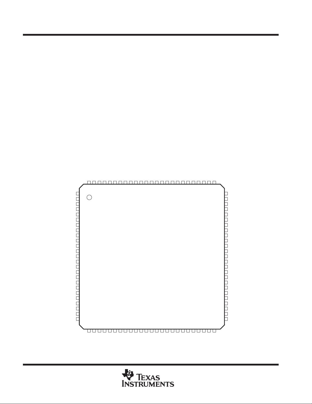
pin assignments
PZP PACKAGE
(TOP VIEW)
GNDLED
OUT0
OUT1
GNDLED
OUT2
OUT3
GNDLED
OUT4
OUT5
GNDLED
OUT6
OUT7
GNDLED
OUT8
OUT9
GNDLED
OUT10
OUT11
GNDLED
OUT12
OUT13
GNDLED
OUT14
OUT15
GNDLED
1
2
3
4
5
6
7
8
9
10
11
12
13
14
15
16
17
18
19
20
21
22
23
24
25
TEST3
TEST2
99
100
27
26
GNDLOG
TEST1
DPOL
DCENA
95
96
97
98
31
30
29
28
BCENA
VCCLOG
DCDIN6
92
93
94
34
33
32
DCDIN5
DCDIN4
DCDIN3
89
90
91
37
36
35
DCDIN2
DCDIN1
DCDIN0
86
87
88
40
38
39
DIN9
DIN8
84
85
42
41
DIN7
DIN6
82
83
44
43
DIN5
DIN4
80
81
46
45
DIN3
DIN2
78
79
48
47
DIN1
DIN0
76
77
50
49
75
74
73
72
71
70
69
68
67
66
65
64
63
62
61
60
59
58
57
56
55
54
53
52
51
VCOIN
RBIAS
MAG0
MAG1
MAG2
PDOUT
GSPOL
GSCLK
BLANK
XENABLE
XOE
DCLK
XLA TCH
DCCLK
XDCLAT
RSEL0
RSEL1
LEDCHK
NC
WDTRG
XDOWN1
XDOWN2
BOUT
XGSOUT
XPOUT
IREF
TSENA
VCCLED
XDWN2TST
2
WDCAP
XDPOUT
GNDANA
POST OFFICE BOX 655303 • DALLAS, TEXAS 75265
VCCANA
DCDOUT0
DCDOUT1
DCDOUT2
DCDOUT3
DCDOUT4
DOUT0
DOUT1
DCDOUT5
DCDOUT6
DOUT2
DOUT3
DOUT4
DOUT5
DOUT6
DOUT7
DOUT8
DOUT9
Page 3
functional block diagram
XOE
BCENA
DCLK
DPOL
XENABLE
DCLK
Control
TLC5911
LED DRIVER
SLLS402 – DECEMBER 1999
DOUT(9–0)
XDPOUT
DIN(9–0),
XLATCH
RSEL(1–0)
DCDIN(6–0),
XDCLAT,
DCCLK
MAG(2–0), GSPOL,
GSCLK, RBIAS,
VCOIN, PDOUT
BLANK
WDCAP
WDTRG
LEDCHK
XDOWN2TST
TSENA
IREF
DCENA
1 x 10 bit B.C.
Data Shift Register
Data Latch
8
PLL
WDT
TSD
10 bit
Clock Countor
16 x 10 bit
Data Shift Register
..........
16 x 10 bit
Data Latch
..........
16 x 10 bit
Data Comparator
..........
16 bit
LED Driver+LOD
..........
16 bit
Current Controller
..........
16 x 7 bit
D.C. Data Latch
XPOUT
XGSOUT
BOUT
OUT0
· · ·
OUT15
XDOWN1
XDOWN2
..........
16 x 7 bit
D.C. Data Shift Register
Legend:
B.C. (Brightness Control): Adjustment for brightness deviation between LED modules, and between panels.
D.C. (Dot Control): Adjustment for brightness deviation between dots.
NOTE: All the input terminals are with Schmitt triggered inverter except RBIAS, VCOIN, PDOUT, IREF and WDCAP.
POST OFFICE BOX 655303 • DALLAS, TEXAS 75265
DCDOUT(6–0)
3
Page 4
TLC5911
CONNECTION
LED DRIVER
SLLS402 – DECEMBER 1999
functional block diagram for shift register and data latch
XOE
DCLK
DPOL
XENABLE
DCCLK
DIN(9–0)
DCDIN(6–0)
XLATCH
XDCLAT
RSEL(1–0)
DCLK
Controller
10
7
DATA
10
a
A
b
B
c
a
A
b
B
c
a
A
b
B
c
S/R
B.C.
S/R
7
D.C.
S/R
10 16 10 16
†
‡
7 16
DATA
LATCH
10 10
10 1010
B.C.
LATCH
7
D.C.
LATCH
7 16
a
b
c
HI–Z
DATA
Comparator
A
H
L
L
H
10
Clock Counter
Current Controller
7 16
10
DOUT(9–0)
DCDOUT(6–0)
DATA
Comparator
7 16
BCENA
DCENA
†
Connecting to 16th 10-bit Bus
‡
Connecting to 16th 7-bit Bus
Legend:
B.C. (Brightness Control): Adjustment for brightness deviation between LED modules, and between panels.
D.C. (Dot Control): Adjustment for brightness deviation between dots.
RSEL
RSEL1 RSEL0
L L A – a, B – c
L H A – b, B – c
H L A – c
H H INHIBIT
Default
4
POST OFFICE BOX 655303 • DALLAS, TEXAS 75265
Page 5
I/O
DESCRIPTION
Á
Á
Á
Á
ÁÁ
ÁÁ
ÁÁ
Á
Á
Á
Á
Á
Á
Á
Á
ÁÁ
ÁÁ
ÁÁ
ÁÁ
Á
Á
Á
ÁÁ
Á
Á
ÁÁ
ÁÁ
Á
ÁÁ
Á
Á
ÁÁ
ÁÁ
Á
Á
Á
ÁÁ
ÁÁ
Á
Á
Á
ÁÁ
ÁÁ
Á
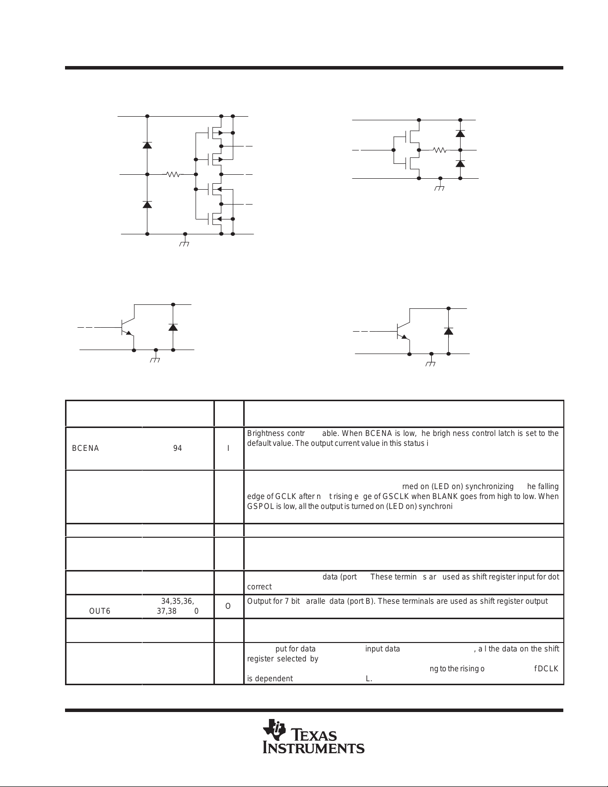
equivalent input and output schematic diagrams
TLC5911
LED DRIVER
SLLS402 – DECEMBER 1999
Input
VCCIF
INPUT
GNDLOG
XDOWN1, XDOWN2
XDOWN1, XDOWN2
GNDLOG
Terminal Functions
DOUT0–9, DCDOUT0–6, XGSOUT, XPOUT, BOUT
VCCLOG
OUTPUT
GNDLOG
OUTn
OUTn
GNDLED
TERMINAL
NAME NO.
ÁÁÁÁ
BCENA
ÁÁÁÁ
ÁÁÁÁ
BLANK
ÁÁÁÁ
ÁÁÁÁ
BOUT
DCCLK
ÁÁÁÁ
DCDIN0 –
DCDIN6
DCDOUT0 –
ÁÁÁÁ
DCDOUT6
DCENA
ÁÁÁÁ
DCLK
ÁÁÁÁ
ÁÁÁÁ
94
ÁÁÁÁ
ÁÁÁÁ
67
ÁÁÁÁ
ÁÁÁÁ
53
62
ÁÁÁÁ
86,87,88,
89,90,91,92
34,35,36,
ÁÁÁÁ
37,38,39,40
95
ÁÁÁÁ
64
ÁÁÁÁ
Brightness control enable. When BCENA is low, the brightness control latch is set to the
ББББББББББББББББББББ
default value. The output current value in this status is 100% of the value set by an external
I
resistor. The frequency division ratio of GSCLK is1/1. When BCENA is high, writing to
ББББББББББББББББББББ
brightness control latch is enabled.
Blank (Light off). When BLANK is high, all output of the constant current driver are turned
ББББББББББББББББББББ
off. When GSPOL is high, all the output is turned on (LED on) synchronizing to the falling
edge of GCLK after next rising edge of GSCLK when BLANK goes from high to low. When
I
ББББББББББББББББББББ
GSPOL is low, all the output is turned on (LED on) synchronizing to the rising edge of GCLK
ББББББББББББББББББББ
after next falling edge of GSCLK when BLANK goes from high to low.
O
BLANK buffered output
Clock input for data transfer. The input data is from DCDIN (port B) . The output data at
DCDOUT . All data on the shift register for dot correction data from DCDIN is shifted by 1 bit
I
ББББББББББББББББББББ
and is synchronized to the rising edge of DCCLK.
Input for 7 bit parallel data (port B). These terminals are used as shift register input for dot
I
correction data.
Output for 7 bit parallel data (port B). These terminals are used as shift register output for
O
ББББББББББББББББББББ
dot correction data.
Latch enable for dot correction data. When DCENA is low, the latch is set to the default value.
I
At this time, the output current value is 100% of the value set by an external resistor.
ББББББББББББББББББББ
Clock input for data transfer. The input data is from DIN (port A) , all the data on the shift
register selected by RSEL0, 1 and the output data at DOUT are shifted by 1 bit and
I
ББББББББББББББББББББ
synchronized to DCLK. Note that whether synchronizing to the rising or falling edge of DCLK
is dependent on the value of DPOL.
POST OFFICE BOX 655303 • DALLAS, TEXAS 75265
5
Page 6
TLC5911
I/O
DESCRIPTION
Á
Á
Á
Á
Á
Á
Á
Á
Á
Á
Á
Á
Á
Á
Á
Á
Á
Á
Á
Á
Á
Á
Á
Á
Á
Á
Á
Á
Á
Á
Á
Á
Á
Á
Á
Á
Á
Á
Á
Á
Á
Á
Á
Á
Á
Á
Á
Á
Á
Á
Á
Á
Á
Á
Á
Á
Á
Á
Á
LED DRIVER
SLLS402 – DECEMBER 1999
TERMINAL
NAME NO.
ÁÁÁÁ
DIN0 – DIN9
ÁÁÁÁ
DOUT0 – DOUT9
ÁÁÁÁ
DPOL
GNDANA
GNDLOG
GNDLED
ÁÁÁÁ
GSCLK
ÁÁÁÁ
ÁÁÁÁ
GSPOL
IREF
ÁÁÁÁ
ÁÁÁÁ
LEDCHK
ÁÁÁÁ
MAG0 – MAG2
NC
OUT0 – DOUT15
ÁÁÁÁ
PDOUT
RBIAS
ÁÁÁÁ
RSEL0
ÁÁÁÁ
RSEL1
ÁÁÁÁ
ÁÁÁÁ
TEST1 – TEST3
THERMAL PAD
TSENA
VCCANA
VCCLOG
VCCLED
VCOIN
WDCAP
ÁÁÁÁ
ÁÁÁÁ
ÁÁÁÁ
ÁÁÁÁ
ÁÁÁÁ
ÁÁÁÁ
ÁÁÁÁ
ÁÁÁÁ
ÁÁÁÁ
ÁÁÁÁ
ÁÁÁÁ
ÁÁÁÁ
ÁÁÁÁ
ÁÁÁÁ
ÁÁÁÁ
Package bottom
ÁÁÁÁ
76,77,78,79,80,
81,82,83,84,85
41,42,43,44,45,
46,47,48,49,50
96
28
98
1,4,7,10,13,
16,19,22,25
68
69
32
58
73,72,71
57
2,3,5,6,8,9,11,
12,14,15,17,18,
20,21,23,24
70
74
60
59
97,99,100
31
33
93
26
75
30
Terminal Functions (Continued)
Input for 10 bit parallel data (port A). These terminals are inputs for shift register for gray
Á
Á
Á
ÁÁББББББББББББББББББББ
Á
Á
Á
Á
Á
Á
Á
Á
Á
Á
Á
ББББББББББББББББББББ
scale data, brightness control, and dot correction data. The register selected is determined
I
by RSEL0, 1.
ББББББББББББББББББББ
Output for 10 bit parallel data (port A). These terminals are outputs for shift register for gray
scale data, brightness control, and dot correction data. The register selected is determined
O
ББББББББББББББББББББ
by RSEL0, 1.
Selects the valid edge of DCLK. When DPOL is high, the rising edge of DCLK is valid. When
I
DPOL is low, the falling edge of DCLK is valid.
Analog ground (Internally connected to GNDLOG and GNDLED)
Logic ground (Internally connected to GNDANA and GNDLED)
LED driver ground (Internally connected to GNDANA and GNDLED)
Clock input for gray scale. When MAG0 through MAG2 are all low, GSCLK is used for pulse
width control. When MAG0 through MAG2 are not low, GSCLK is used for PLL timing control.
I
ББББББББББББББББББББ
The gray scale display is accomplished by lighting the LED until the number of GSCLK or
PLL clocks counted is equal to the data latched.
ББББББББББББББББББББ
Select the valid edge of GSCLK. When GSPOL is high, the rising edge of GSCLK is valid.
I
When GSPOL is low, the falling edge of GSCLK is valid.
Constant current value setting. LED current is set to the desired value by connecting an
external resistor between IREF and GND. The 38 times current is compared to current
I/O
ББББББББББББББББББББ
across the external resistor sink on the output terminal.
LED disconnection detection enable. When LEDCHK is high, the LED disconnection
ББББББББББББББББББББ
detection is enabled and XDOWN2 is valid. When LEDCHK is low, the LED disconnection
I
detection is disabled.
ББББББББББББББББББББ
PLL multiple ratio setting. The clock frequency generated by PLL referenced to GSCLK is
I
set .
No internal connection
O
Constant current output
ББББББББББББББББББББ
I/O
Resistor connection for PLL feedback adjustment
I/O
Resistor connection for PLL oscillation frequency setting
Input/output port selection and shift register data latch switching.
When RSEL1 is low and RSEL0 is low, the gray scale data shift register latch is selected to
ББББББББББББББББББББ
port A, and the dot correction register latch is selected to port B.
ББББББББББББББББББББ
When RSEL1 is low and RSEL0 is high, the brightness control register latch is selected to
I
port A, and the dot correction register latch is selected to port B.
ББББББББББББББББББББ
When RSEL1 is high and RSEL0 is low, the dot correction register latch is selected to port A
ББББББББББББББББББББ
and no register latch is selected to port B.
I
TEST. Factory test terminal. These terminals should be connected to GND.
Heat sink pad. This pad is connected to the lowest potential IC or thermal layer.
I
TSD enable. When TSENA is high, TSD is enabled. When TSENA is low, TSD is disabled.
Analog power supply voltage
Logic power supply voltage
LED driver power supply voltage
I/O
Capacitance connection for PLL feedback adjustment
WDT detection time adjustment. WDT detection time is adjusted by connecting a capacitor
between WDCAP and GND. When WDCAP is directly connected to GND, the WDT function
I/O
ББББББББББББББББББББ
is disabled. In this case, WDTRG should be tied to high or low level.
6
POST OFFICE BOX 655303 • DALLAS, TEXAS 75265
Page 7
I/O
DESCRIPTION
Á
Á
Á
Á
ÁÁ
ÁÁ
ÁÁ
Á
Á
Á
Á
ÁÁ
ÁÁ
Á
Á
Á
ÁÁ
ÁÁ
Á
Á
Á
ÁÁ
ÁÁ
Á
Á
Á
ÁÁ
ÁÁ
Á
Á
Á
ÁÁ
ÁÁ
Á
Á
Á
ÁÁ
ÁÁ
Á
Á
Á
ÁÁ
ÁÁ
Á
Á
Á
ÁÁ
ÁÁ
Á
TERMINAL
NAME NO.
ÁÁÁÁ
WDTRG
ÁÁÁÁ
XDCLAT
ÁÁÁÁ
XDOWN1
ÁÁÁÁ
XDOWN2
ÁÁÁÁ
XDPOUT
XDWN2TST
ÁÁÁÁ
XENABLE
ÁÁÁÁ
XGSOUT
ÁÁÁÁ
XLATCH
ÁÁÁÁ
XOE
ÁÁÁÁ
XPOUT
ÁÁÁÁ
56
ÁÁÁÁ
61
ÁÁÁÁ
55
ÁÁÁÁ
54
ÁÁÁÁ
29
27
ÁÁÁÁ
66
ÁÁÁÁ
52
ÁÁÁÁ
63
ÁÁÁÁ
65
ÁÁÁÁ
51
LED DRIVER
SLLS402 – DECEMBER 1999
Terminal Functions (Continued)
WDT trigger input. By applying a scan signal to this terminal, the scan signal can be
ББББББББББББББББББББ
monitored by turning the constant current output off and protecting the LED from the damage
I
of burning when the scan signal stops during the constant period designed.
ББББББББББББББББББББ
Data latch for dot correction. When XDCLAT is high, data on the shift register for dot
correction data from DCDIN (port B) goes through latch. When XDCLAT is low, the data is
I
ББББББББББББББББББББ
latched. Accordingly , if data on the shift register is changed during XDCLAT high, the new
value is latched (level latch).
Shutdown. XDOWN1 is configured as open collector. It goes low when the constant current
O
ББББББББББББББББББББ
output is shut down by the WDT or TSD function.
LED disconnection detection output. XDOWN2 is configured as open collector. XDOWN2
O
goes low when a LED disconnection is detected.
ББББББББББББББББББББ
O
DPOL output inverted
T est for XDOWN2. When XDWN2TST is low, XDOWN2 goes low . (This terminal is internally
I
ББББББББББББББББББББ
pulled up with 50 kΩ)
DCLK enable. When XENABLE is low, data transfer is enabled. Data transfer starts on the
I
valid edge of DCLK after XENABLE goes low. During XENABLE high, no data is transferred.
ББББББББББББББББББББ
Clock output for gray scale. When MAG0 through MAG2 are all low, a clock with GSCLK
inverted appears on this terminal. When MAG0 through MAG2 are not low., PLLCLK
O
ББББББББББББББББББББ
appears on this terminal.
Latch. When XLATCH is high, data on shift register from DIN (port A) goes through latch.
When XLATCH is low , data is latched. Accordingly , if the data on the shift register is changed
I
ББББББББББББББББББББ
during XLA TCH high, this new value is latched (level latch).
Data output enable. When XOE is low, the DOUT0–9 terminals are driven. When XOE is
I
high, the DOUT0–9 terminals go to a high-impedance state.
ББББББББББББББББББББ
O
GSPOL output inverted
TLC5911
POST OFFICE BOX 655303 • DALLAS, TEXAS 75265
7
Page 8
TLC5911
Á
Á
Á
Á
Á
Á
Á
Á
Á
Á
Á
Á
Á
Á
Á
Á
Á
Á
Á
Á
Á
Á
Á
Á
Á
Á
Á
Á
Á
Á
Á
Á
mA
LED DRIVER
SLLS402 – DECEMBER 1999
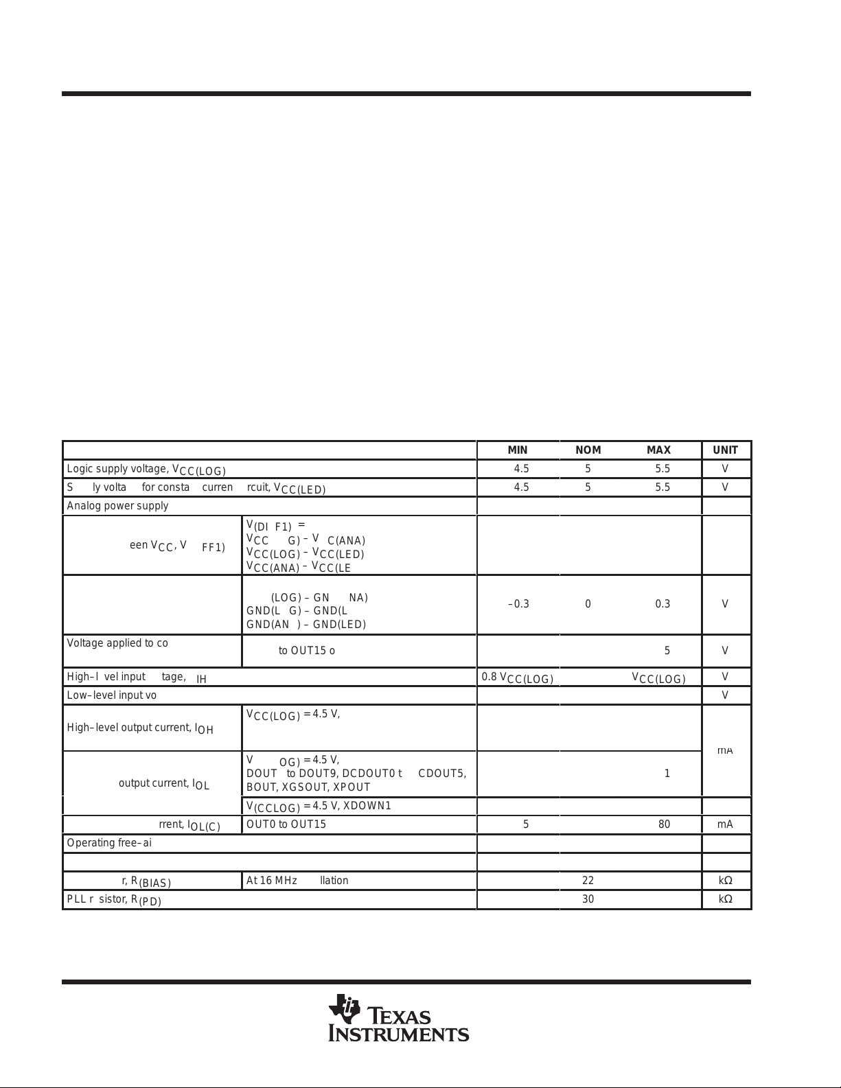
absolute maximum ratings over operating free-air temperature (unless otherwise noted)
Logic supply voltage, V
CC(LOG)
Supply voltage for constant current circuit, V
Analog supply voltage, V
Output current (DC), I
CC(ANA)
OL(C)
– 0.3 V to 7 V. . . . . . . . . . . . . . . . . . . . . . . . . . . . . . . . . . . . . . . . . . . . . . . . . . . . .
CC(LED)
– 0.3 V to 7 V. . . . . . . . . . . . . . . . . . . . . . . . . . . . . . . . . . .
– 0.3 V to 7 V. . . . . . . . . . . . . . . . . . . . . . . . . . . . . . . . . . . . . . . . . . . . . . . . . . . .
85 mA. . . . . . . . . . . . . . . . . . . . . . . . . . . . . . . . . . . . . . . . . . . . . . . . . . . . . . . . . . . . . . .
†
Input voltage range, VI – 0.3 V to VCCLOG + 0.3 V. . . . . . . . . . . . . . . . . . . . . . . . . . . . . . . . . . . . . . . . . . . . . . . . .
Output voltage range, V
(DOUT)
Output voltage range, VO and V
Storage temperature range, T
, V
(DCDOUT)
(XDOWNn)
–40°C to 150°C. . . . . . . . . . . . . . . . . . . . . . . . . . . . . . . . . . . . . . . . . . . . . . . . . . .
str
, V
(BOUT)
, V
(XPOUT)
and V
(XGSOUT)
– 0.3 V to VCCLOG + 0.3 V
– 0.3 V to 16 V. . . . . . . . . . . . . . . . . . . . . . . . . . . . . . . . . . . . . . . . . . .
Continuous total power dissipation at (or below) TA = 25°C 4.7 W. . . . . . . . . . . . . . . . . . . . . . . . . . . . . . . . . . . .
Power dissipation rating at (or above) TA = 25°C 38.2m W/°C. . . . . . . . . . . . . . . . . . . . . . . . . . . . . . . . . . . . . . .
†
Stresses beyond those listed under “absolute maximum ratings” may cause permanent damage to the device. These are stress ratings only, and
functional operation of the device at these or any other conditions beyond those indicated under “recommended operating conditions” is not
implied. Exposure to absolute-maximum-rated conditions for extended periods may affect device reliability.
NOTE 1: All voltage values are with respect to GNDLOG terminal.
recommended operating conditions
dc characteristics
Logic supply voltage, V
CC(LOG)
Supply voltage for constant current circuit, V
Analog power supply, V
ББББББББ
Voltage between VCC, V
ББББББББ
Voltage between GND, V
ББББББББ
ББББББББ
Voltage applied to constant current
output, V
O
High–level input voltage, V
Low–level input voltage, V
High–level output current, I
ББББББББ
ББББББББ
Low–level output current, I
Constant output current, I
Operating free–air temperature range, T
PLL capacitance, C
PLL resistor, R
PLL resistor, R
(BIAS)
(PD)
CC(ANA)
(VCO)
(DIFF1)
(DIFF2)
IH
IL
OH
OL
OL(C)
V
(DIFF1)
V
CC(LOG)
ББББББББББ
V
CC(LOG)
ББББББББББ
V
CC(ANA)
V
(DIFF2)
GND(LOG) – GND(ANA)
ББББББББББ
GND(LOG) – GND(LED)
GND(ANA) – GND(LED)
ББББББББББ
OUT0 to OUT15 off
V
CC(LOG)
DOUT0 to DOUT9, DCDOUT0 to DCDOUT5,
ББББББББББ
BOUT, XGSOUT, XPOUT
V
CC(LOG)
DOUT0 to DOUT9, DCDOUT0 to DCDOUT5,
ББББББББББ
BOUT, XGSOUT, XPOUT
V
(CCLOG)
OUT0 to OUT15
A
At 16 MHz oscillation
CC(LED)
=
– V
CC(ANA)
– V
CC(LED)
– V
CC(LED)
=
= 4.5 V,
= 4.5 V,
= 4.5 V, XDOWN1, XDOWN2
MIN
4.5
4.5
4.5
ÁÁÁ
–0.3
ÁÁÁ
–0.3
ÁÁÁ
ÁÁÁ
0.8 V
CC(LOG)
GND(LOG)
ÁÁÁÁÁÁÁÁÁÁ
ÁÁÁÁÁÁÁÁÁÁ
5
–20
NOM
5
5
5
ÁÁ
0
ÁÁ
0
ÁÁ
ÁÁ
1
22
30
MAX
5.5
5.5
5.5
ÁÁÁ
0.3
ÁÁÁ
0.3
ÁÁÁ
ÁÁÁ
15
V
CC(LOG)
0.2 V
CC(LOG)
–1
1
5
80
85
UNIT
V
V
V
Á
V
Á
V
Á
Á
V
V
V
Á
Á
mA
mA
°C
µF
kΩ
kΩ
8
POST OFFICE BOX 655303 • DALLAS, TEXAS 75265
Page 9
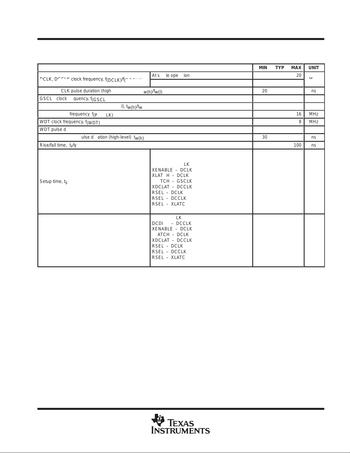
DCLK, DCCLK clock frequenc
f
MH
Á
Á
Á
Á
Á
Á
Á
Á
Á
Á
Á
Á
Á
Á
Á
Á
Á
Á
Á
Á
Á
Á
Á
Á
Á
Á
Á
Á
Á
Á
Á
Á
Á
Á
Á
Á
Á
Á
Á
Á
Á
Á
Á
Á
Á
Á
Á
Á
Á
Á
Á
Á
Á
Á
Á
Á
Á
Á
Á
Á
Á
Á
Á
Á
Á
Á
Á
Á
Á
Á
Á
Á
recommended operating conditions (continued)
TLC5911
LED DRIVER
SLLS402 – DECEMBER 1999
ac characteristics, V
CC(LOG)
= V
CC(ANA)
y,
(DCLK)/f(DCCLK)
DCLK, DCCLK pulse duration (high- or low-level), t
GSCLK clock frequency, f
GSCLK pulse duration (high- or low-level), t
PLLCLK clock frequency, f
WDT clock frequency, f
WDT pulse duration (high- or low-level), t
(GSCLK)
w(h)/tw(l)
(PLLCLK)
(WDT)
w(h)/tw(l)
XLATCH, XDCLAT pulse duration (high-level), t
Rise/fall time, tr/t
ББББББББББББ
ББББББББББББ
ББББББББББББ
Setup time, t
ББББББББББББ
ББББББББББББ
ББББББББББББ
ББББББББББББ
ББББББББББББ
ББББББББББББ
Hold time, t
ББББББББББББ
ББББББББББББ
ББББББББББББ
f
su
h
= V
CC(LED)
At single operation
At cascade operation
w(h)/tw(l)
w(h)
DINn – DCLK
DCDINn – DCCLK
BLANK – GSCLK
XENABLE – DCLK
XLATCH – DCLK
XLATCH – GSCLK
XDCLAT – DCCLK
RSEL – DCLK
RSEL – DCCLK
RSEL – XLATCH
RSEL – XDCLAT
DINn – DCLK
DCDINn – DCCLK
XENABLE – DCLK
XLATCH – DCLK
XDCLAT – DCCLK
RSEL – DCLK
RSEL – DCCLK
RSEL – XLATCH
RSEL – XDCLAT
= 4.5 V to 5.5 V, T A = – 20 to 85°C (unless otherwise noted)
MIN
TYP
20
40
40
30
ББББББББББ
ББББББББББ
ББББББББББ
ББББББББББ
ББББББББББ
ББББББББББ
ББББББББББ
ББББББББББ
ББББББББББ
ББББББББББ
ББББББББББ
ББББББББББ
Á
Á
Á
Á
Á
Á
Á
Á
Á
Á
Á
Á
10
15
10
10
10
10
15
30
15
15
15
20
30
20
20
20
20
10
5
Á
5
Á
Á
Á
Á
Á
Á
Á
Á
Á
Á
Á
MAX
100
Á
Á
Á
Á
Á
Á
Á
Á
Á
Á
Á
Á
20
15
16
UNIT
z
ns
8
MHz
ns
MHz
8
MHz
ns
ns
ns
Á
Á
Á
ns
Á
Á
Á
Á
Á
Á
ns
Á
Á
Á
POST OFFICE BOX 655303 • DALLAS, TEXAS 75265
9
Page 10

TLC5911
Á
Á
Á
Á
Á
Á
Á
Á
Á
Á
OL
g
Á
Á
Á
Á
Á
Á
Á
Á
Á
Á
Á
Á
Á
Á
Á
Á
Á
Á
I
Á
Supply current (logic)
Á
Á
Á
Á
mA
Á
Á
Á
Á
I
Supply current (analog)
mA
Á
Á
Á
Á
Á
Á
Á
Á
Á
Á
Á
I
OL(K)
Constant out ut leakage current
Á
Á
Á
Á
Á
Á
Á
Á
Á
Á
Á
Á
Á
Á
Á
Á
Á
Á
LED DRIVER
SLLS402 – DECEMBER 1999
electrical characteristics, LEDCHK = L, MIN/MAX: V
= –20 to 85°C, TYP: V
T
A
PARAMETER
V
ÁÁÁ
OH
High-level output voltage
ББББББББ
CC(LOG)
= V
CC(ANA)
= V
CC(LED)
TEST CONDITIONS
IOH = –1 mA, DOUTn, DCOUTn, XGSOUT,
ББББББББББ
XPOUT, BOUT
CC(LOG)
= V
CC(ANA)
= 5 V , TA = 25°C (unless otherwise noted)
IOL = 1 mA, DOUTn, DCOUTn, XGSOUT,
V
ÁÁÁ
Low-level output voltage
ББББББББ
XPOUT, BOUT
ББББББББББ
IOL = 5 mA, XDOWN1, XDOWN2
I
I
Input current
VI = V
CC(LOG)
or GND(LOG)
Input signal is static,
ÁÁÁÁББББББББÁББББББББББ
TSENA = H, WDCAP = OPEN,
No PLL is used
ÁÁÁ
ÁÁÁ
(LOG)
ББББББББ
ББББББББ
pp
Input signal is static,
ББББББББББ
TSENA = H, WDCAP = OPEN,
PLL multiple ratio = 1042
ББББББББББ
Data transfer,
DCLK = 20 MHz, GSCLK = 8 MHz
ÁÁÁ
ББББББББ
ББББББББББ
No PLL is used
Data transfer,
ÁÁÁÁББББББББÁББББББББББ
(ANA)
I
(LED)
ÁÁÁÁББББББББÁББББББББББ
I
OL(C1)
I
OL(C2)
ÁÁÁ
pp
Supply current
(constant current driver)
Constant output current
(includes error between bits)
Constant output current
ББББББББ
(includes error between bits)
p
∆I
ÁÁÁ
OL(C)
I∆
OL(C1)
ÁÁÁ
I∆
OL(C2)
T
(tsd)
T
(wdt)
V
(IREF)
V
(LEDDET)
ÁÁÁ
P
(LLJITTER)
Constant output current error
ББББББББ
between bit
Changes in constant output current
ББББББББ
depend on supply voltage
Changes in constant output current
depend on output voltage
TSD detection temperature
WDT detection temperature
Voltage reference
Voltage applied to LED
disconnection detection
ББББББББ
PLL jitter
DCLK = 20 MHz, GSCLK = 15 kHz
PLL multiple ratio = 1042
BLANK = L, R
BLANK = L, R
LED turn off, R
LED turn off, R
VO = 1 V, R
all output bits turn on
VO = 1 V, R
all output bits turn on
VO = 1 V, V
R
(IREF)
(IREF)
(IREF)
(IREF)
= 1200 W
VO = 0.7 V, V
ББББББББББ
R
= 600 W
(IREF)
OUT0 to OUT15 (V
XDOWN1, 2 (V
(IREF)
(IREF)
(IREF)
(IREF)
= 1200 Ω
= 600 Ω
= 1.2 V,
(IREF)
OUTn
XDOWNn
= 1200 Ω
= 600 Ω
= 1200 Ω
= 600 Ω
= 1.2 V
= 15 V)
= 15 V)
DOUTn, DCDOUTn
(V
= VCCLOG or GND)
OUTn
V
CC(LOG)=VCC(ANA)=VCC(LED)
VO = 1 V, R
ББББББББББ
All output bits turn on
VO = 1 V, R
ББББББББББ
V
= 1.2 V
IREF
VO = 1 V to 3 V, R
V
= 1.2 V, 1 bit output turn on
IREF
(IREF)
(IREF)
= 600 W
= 600 W,
= 600 Ω,
(IREF)
Junction temperature
No external capacitor
BCENA = L, R
ББББББББББÁÁÁ
R
= 22 kΩ, R
(BIAS)
C
= 0.1 µF
(VCO)
(IREF)
= 9.6 kΩ,
= 30 kΩ,
(PD)
= V
CC(LED)
MIN
V
CC(LOG)
ÁÁ
–0.5
ÁÁÁÁÁÁ
ÁÁÁÁÁÁ
ÁÁ
ÁÁ
= 4.5 V to 5.5 V ,
TYP
ÁÁÁÁÁ
Á
Á
35
ÁÁÁÁ
ÁÁÁÁ
39
6.5
13
12
20
12
ÁÁÁÁ
35
70
ÁÁ
ÁÁÁÁ
ÁÁÁÁ
20
40
80
Á
± 1%
± 1%
± 1%
150
5
160
10
1.2
0.2
0.3
Á
0.4%
MAX
0.5
0.5
±1
Á
Á
45
Á
49
Á
15
20
35
20
35
Á
45
90
Á
0.1
± 4%
Á
± 4%
Á
± 3%
170
15
0.4
Á
2%
UNIT
V
V
Á
µA
Á
1
mA
Á
3
Á
Á
mA
Á
8
mA
Á
mA
mA
Á
µA
1
µA
1
µA
Á
V
Á
V
°C
ms
V
V
Á
10
POST OFFICE BOX 655303 • DALLAS, TEXAS 75265
Page 11

tdPropagation delay time
ns
TLC5911
LED DRIVER
SLLS402 – DECEMBER 1999
switching characteristics, CL = 15 pF , MIN/MAX: V
= –20 to 85°C, TYP: V
PARAMETER
trRise time
tfFall time
p
NOTES: 2. MAG0 to MAG2 are all low level.
3. Until DOUT is turned on (drive) or turned off (Hi-Z).
CC(LOG)
= V
= V
CC(ANA)
CC(LED)
DOUTn, DCDOUTn
XGSOUT, BOUT, XPOUT
OUTn (see Figure 1)
DOUTn, DCDOUTn
XGSOUT, BOUT, XPOUT
OUTn (see Figure 1)
OUTn+1 – OUTn
BLANK↑ – OUT0
BLANK – BOUT
GSCLK – OUT0 (see Note 2)
GSCLK – XGSOUT
DCLK – DOUTn
DCLK – DCDOUTn
DCCLK – DCDOUTn
XOE↓ – DOUTn (see Note 3)
XOE↑ – DOUTn (see Note 3)
RSEL – DOUTn
LEDCHK – XDOWN2
CC(LOG)
= V
CC(ANA)
= V
CC(LED)
= 4.5 V to 5.5 V , T
= 5 V, TA = 25°C (unless otherwise noted)
TEST CONDITIONS
MIN
40
10
10
15
15
15
10
10
10
TYP
12
12
110
10
10
130
30
50
20
7
20
30
30
30
20
15
20
MAX
30
30
30
30
45
70
40
40
45
45
45
35
25
40
1000
A
UNIT
ns
ns
POST OFFICE BOX 655303 • DALLAS, TEXAS 75265
11
Page 12

TLC5911
LED DRIVER
SLLS402 – DECEMBER 1999
PARAMETER MEASUREMENT INFORMATION
V
CC
90%
10%
100%
50%
0%
51 Ω
15 pF
600 Ω
V
CC
IREF OUTn
GND
Figure 1. Rise Time and Fall Time Test Circuit for OUTn
100%
50%
0%
V
IH
V
IL
100%
50%
0%
t
r
t
w(h)
V
IH
V
t
f
t
IL
w(l)
VIH or V
VIL or V
t
d
OH
OL
VIH or V
VIL or V
OH
OL
Figure 2. Timing Requirements
12
POST OFFICE BOX 655303 • DALLAS, TEXAS 75265
Page 13

LED DRIVER
SLLS402 – DECEMBER 1999
PRINCIPLES OF OPERATION
setting for output constant current value
On the constant current output terminals (OUT0–15), approximately 38 times the current which flows through
the external resistor, R
calculated using the following equation:
(connected between IREF and GND), can flow. The external resistor value is
(IREF)
TLC5911
R
(Ω) ≅ 38 × 1.2 (V) / I
(IREF)
(A) where both BCENA and DCENA are low.
OL(C)
Note that more current flows if IREF is connected to GND directly.
constant output current operation
The constant current output turns on (sink constant current), if GSPOL is high and if all the gray scale data
latched into the gray scale latch is not zero on the falling edge of the gray scale clock after the next rising edge
of the gray scale clock when BLANK goes from high to low. After that, the number of the falling edge is counted
by the 10-bit gray scale counter. Then, the output counted corresponding to the gray scale data is turned off
(stop to sink constant current). The gray scale clock can be selected, as discussed in later section, from GSCLK
or by internal PLL circuitry. If the shift register for the gray scale is updated during XLATCH high, the data on
the gray scale data latch is also updated affecting the number of the gray scale of constant current output.
Accordingly , during the on-state of the constant current output, XLATCH should be kept at a low level and the
gray scale data latch should be held.
input/output port and shift register selection
The TLC5911 supplies two parallel input ports such as DIN (10 bits : port A) and DCDIN (7 bits: port B). The
DIN and DCDIN ports also supply DCLK and DCCLK for the shift clock, XLATCH and XDCLAT for latch, and
DOUT and DCDOUT for output, respectively . The device has three kinds of shift register latchs such as the gray
scale data, brightness control, and dot correction. The port and shift registers can be selected by RSEL0 and
RSEL1. The selection of the shift registers will be done by RESL0 and RSEL1 as shown in Table 1. Note that
the RSELn setting is done at DCLK low and DPOL high (DCLK is high when DPOL is low). When only port A
is used, DCDIN, DCDOUT, DCCLK, and XDCLAT should be connected to GND.
Table 1. Shift Register Latch Selection
SELECTED SHIFT REGISTER LATCH
PORT A
RSEL1
L
L
H
H
NOTE 4: Zero is output to DOUT7 through DOUT9.
RSEL0
L
H
L
H
DIN, DCLK, XLATCH, DOUT
Gray scale data displayed
Brightness control
Dot correction (see Note 4)
N/A (inhibit)
DCDIN, DCCLK, XDCLAT
Dot correction
Dot correction
Not connected
N/A (inhibit)
PORT B
DCDOUT
Dot correction
Dot correction
Dot correction
N/A (inhibit)
shift register latch for gray scale data
The shift register latch for the gray scale data is configured with 16 × 10 bits. The gray scale data, configured
with 10 bits, represents the time when constant current output is being turned on, and the data range is 0 to 1023
(00h to 3FFh). When the gray scale data is 0, the time is shortest, and the output is not turned on (light off). On
the other hand, when the gray scale data is 1023, the time is longest, and it turns on during the time of the 1023
clocks from the gray scale clock. The configuration of the shift register and the latch for gray scale data is shown
in Figure 3.
POST OFFICE BOX 655303 • DALLAS, TEXAS 75265
13
Page 14

TLC5911
)
LED DRIVER
SLLS402 – DECEMBER 1999
Latch for Gray Scale Data
PRINCIPLES OF OPERATION
XLATCH
DOUT0 to 9
OUT15
Data
(10 bits)
Shift Register for Gray Scale Data
16th byte
DIN9 MSB
DIN0 LSB
OUT14
Data
(10 bits)
15th byte
DIN9 MSB
DIN0 LSB
OUT1
Data
(10 bits)
2nd byte
DIN9 MSB
DIN0 LSB
OUT0
Data
(10 bits)
1st byte
DIN9 MSB
DIN0 LSB
Figure 3. Relationship Between Shift Register and Latch for Gray Scale Data
shift register latch for brightness control
The shift register latch for brightness control is configured with 1 × 10 bits. Using the shift register latch for the
brightness control, the division ratio of the gray scale clock can be set and the output current value on constant
current output can be adjusted. When powered up, the latch data is indeterminate and the shift register is not
initialized. When these functions are used, data should be written to the shift register latch prior to lighting-on
(BLANK=L). Also, it is prohibited from rewriting the latch value for the brightness control when the constant
current output is turned on. When these functions are not used, the latch value can be set to the default value
setting of BCENA at low level (connect to GND). Also, DIN9 is assigned to the LSB of the reference current
control to maintain compatibility with the TLC5901/02/03 family . The configuration of the shift register and the
latch for brightness control is shown in Figure 4.
Latch for Brightness Control
DCLK
DIN0 to 9
Gray Scale Clock Division Ratio Data Set
XLATCH
DOUT0 to 9
NOTE A: Indicates default value at BCENA low.
00 1111
MSB LSB MSB LSB
Shift Register for Brightness Control
DIN8
DATA
DIN7
DATA
00
DIN6
DATA
DIN5
DATA
Current Data Adjusted On Constant Current Output
11
DIN4
DATA
DIN3
DATA
DIN2
DATA
DIN1
DATA
DIN0
DATA
DIN9
DATA
Figure 4. Relationship Between Shift Register and Latch for Brightness Control
shift register latch for dot correction
The shift register latch for dot correction is configured with 16 × 7 bits. Using the shift register latch for dot
correction, the current value on the constant current output can be set individually . When powered up, the latch
data is indeterminate and the shift register is not initialized. When these functions are used, data should be
written to the shift register latch prior to lighting-on (BLANK=L). Also, rewriting the latch value for dot correction
when the constant current output is turned on is inhibited. When these functions are not used, the latch value
can be set to the default value setting of DCENA at low level (connect to GND). The configuration of the shift
register and the latch for dot correction is shown in Figure 5.
(see Note A
DCLK
DIN0 to 9
14
POST OFFICE BOX 655303 • DALLAS, TEXAS 75265
Page 15

6
TLC5911
LED DRIVER
SLLS402 – DECEMBER 1999
PRINCIPLES OF OPERATION
Latch for Dot Correction
XDCLAT
DCDOUT0 to 6
XLATCH
DOUT0 to 6
OUT15
Data
(7 bits)
Shift Register for Dot Correction
16th byte
DCDIN6 MSB
DCDIN0 LSB
Latch for Dot Correction
OUT15
Data
(7 bits)
Shift Register for Dot Correction
16th byte
DIN6 MSB
DIN0 LSB
OUT14
Data
(7 bits)
15th byte
DCDIN6 MSB
DCDIN0 LSB
Using Port B (RSEL0=L or H, RSEL1=L)
OUT14
Data
(7 bits)
15th byte
DIN6 MSB
DIN0 LSB
OUT1
Data
(7 bits)
2nd byte
DCDIN6 MSB
DCDIN0 LSB
OUT1
Data
(7 bits)
2nd byte
DIN6 MSB
DIN0 LSB
OUT0
Data
(7 bits)
1st byte
DCDIN6 MSB
DCDIN0 LSB
OUT0
Data
(7 bits)
1st byte
DIN6 MSB
DIN0 LSB
DCCLK
DCDIN0 to
DCLK
DIN0 to 6
Using Port A (RSEL0=L, RSEL1=H)
Figure 5. Relationship Between the Shift Register and the Latch for Dot Correction
write data to shift register latch
The shift register latch written is selected using the RSEL0 and RSEL1 terminal. At port A, the data is applied
to the DIN data input terminal, clocked into the shift register and synchronized to the rising edge of DCLK after
XENABLE is pulled low. At port B, the data is applied to the DCDIN data input terminal, clocked into the shift
register, and synchronized to the rising edge of DCCLK. The shift register for the gray scale data is configured
with 16 × 10 bits and the shift register for dot correction is configured with 16 × 7 bits resulting in sixteen times
DCLK. The shift register for the brightness control is configured with 1 × 10 bits resulting in one times DCLK.
At the number of DCLK input for each case, data can be written into the shift register. In this condition, when
the XLA TCH at port A or the XDCLAT at port B is pulled high, data in the shift register is clocked into the latch
(data through). When the XLATCH at port A or XDCLAT at port B is pulled low, data is held (latch).
POST OFFICE BOX 655303 • DALLAS, TEXAS 75265
15
Page 16

TLC5911
Á
Á
Á
Á
Á
Á
Á
Á
Á
Á
Á
Á
Á
Á
Á
Á
Á
Á
Á
Á
Á
Á
Á
Á
LED DRIVER
SLLS402 – DECEMBER 1999
PRINCIPLES OF OPERATION
brightness control function
By writing data into the brightness control latch, current on all the constant current outputs can be adjusted to
control the variation of brightness between ICs. The division ratio for the gray scale clock can be set to control
the variation of brightness for the total panel system. Furthermore, by writing data into the dot correction latch,
current on each constant current output can be adjusted.
output current adjustment on all constant current outputs – brightness adjustment between ICs
By using the lower 6 bits of the brightness control latch, output current can be adjusted in 64 steps as 1 step
of 0.8% of the current ratio between 100% and 50.8% when the output current is set to 100% of an external
resistor (note that the current value is lower if the constant current output is corrected using the dot correction
function). By using this function, the brightness control between modules (ICs) can be adjusted sending the
desired data externally even if ICs are mounted on a print-circuit board. When BCENA is pulled low, the output
current is set to 100%.
Table 2. Relative Current Ratio For Total Constant Current Output
CURRENT RATIO
%
ÁÁÁÁ
50.8
ÁÁÁÁ
ÁÁÁÁ
.
.
.
.
99.2
100
†
BCENA is low.
20 (mA)
ÁÁÁ
10.2
.
ÁÁÁ
.
.
ÁÁÁ
.
19.8
20.0
80 (mA)
ÁÁÁ
40.6
.
ÁÁÁ
.
.
ÁÁÁ
.
79.7
80.0
CODE
БББББ
MSB 000000 LSB
БББББ
БББББ
.
.
.
.
111110
†
111111
V
IREF
(TYP)
ÁÁ
0.60
.
ÁÁ
.
.
ÁÁ
.
1.19
1.20
frequency division ratio setting for gray scale clock – panel brightness adjustment
By using the upper 4 bits of the brightness control latch, the gray scale clock can be divided into 1/1 to 1/16.
If the gray scale clock is set to 16 times the speed of frequency (1024×16=16384) during horizontal scanning
time, the brightness can be adjusted in 16 steps by selecting the frequency division ratio. By using this function,
the total panel brightness can be adjusted at once, and applied to the brightness of day or night. When BCENA
is pulled low, the gray scale clock is not divided. When BCENA is pulled high, the brightness can be adjusted
as shown in Table 3.
Table 3. Relative Brightness Ratio For Total Constant Current Output
RELATIVE
BRIGHTNESS RATIO
БББББ
(%)
6.3
.
БББББ
БББББ
.
.
.
93.8
100
CODE
БББББ
MSB 0000 LSB
†
.
БББББ
БББББ
.
.
.
1110
1111
†
BCENA is low.
FREQUENCY DIVISION
ББББББ
RATIO
1/1
.
ББББББ
ББББББ
.
.
.
1/15
1/16
16
POST OFFICE BOX 655303 • DALLAS, TEXAS 75265
Page 17

Á
Á
Á
Á
Á
Á
LED DRIVER
SLLS402 – DECEMBER 1999
PRINCIPLES OF OPERATION
output current adjustment on each constant current output – LED brightness adjustment
By using the dot correction latch, the output current on each constant current output can be adjusted in 128 steps
as 1 step of 0.8% of the current ratio between 100% and 0% when the output current is set to 100% of an external
resistor at 7Fh of the latched value and the lower 6 bits of the brightness control register. By using this function,
the brightness deviation from the LED brightness variation can be minimized. When DCENA is pulled low , the
output current is set to 100% without the dot correction.
Table 4. Relative Current Ratio By Constant Current Output
TLC5911
CODE
MSB 0000000 LSB
.
ÁÁÁÁ
ÁÁÁÁ
.
.
.
1111110
†
1111111
†
DCENA is low.
CURRENT RATIO %
0.0
.
БББББ
БББББ
.
.
.
99.2
100
I
=40 (mA)
OL(C)
0.0
.
ÁÁÁÁ
ÁÁÁÁ
.
.
.
39.7
40
clock edge selection
The high speed clock signal is diminished due to the duty ratio change through the multiple stages of the IC or
module as shown in Figure 6.
A’IN A OUT IN A OUT OUT’
IN
A
OUT
IN’
A’
OUT
a) Propagate through multiple stages buffer
b) Insert inverter between buffers
with slow falling edge
Figure 6. Clock Edge Selection
In Figure 6a, if the falling edge at the internal buffer is behind the rising edge, the clock will disappear if a multiple
cascade connection is made. To resolve this problem, the duty ratio can be held unchanged using the
connection as shown in Figure 6b if the valid clock edge can be selected (arrow in Figure 6). Note that the clock
delay is not avoided even in this case.
The device incorporates the clock edge selection function for each DCLK and GSCLK. By using this function,
the falling edge or rising edge for the valid edge can be selected depending on the status of DPOL and GSPOL,
thus the degradation for the duty ratio can be reduced. The relationship between each signal is shown in T able 5.
POST OFFICE BOX 655303 • DALLAS, TEXAS 75265
17
Page 18

TLC5911
(Gray scale clock is internally generated)
LED DRIVER
SLLS402 – DECEMBER 1999
PRINCIPLES OF OPERATION
Table 5. Valid Edge For DCLK and GSCLK
DPOL
H
L
GSPOL
H
L
DCLK valid edge
DCLK↑
DCLK↓
GSCLK valid edge
GSCLK↑
GSCLK↓
Operation at XENABLE = H
Pull DCLK to low level
Pull DCLK to high level
PLL operation
Synchronize to the high level of DCLK
Synchronize to the low level of DCLK
The device supplies the XPOUT and XGSOUT output terminals for the cascade operation which inverts GSPOL
and GSCLK respectively . It also supplies the BOUT output terminal as a buffered BLANK to make timing easy
with GSCLK and XGSOUT.
gray scale clock generation
When MAG<0:2> are all low, the clock input from the GSCLK terminal is used as the gray scale clock with no
change, and except for this case the internal PLL generates the clock for the gray scale control clock. When
using the PLL, the gray scale clock is generated by adjusting the clock to have the same number of pulses as
the multiple ratio of the GSCLK reference period (when GSCLK and GSPOL are kept at the same level). The
ratio in this case is determined depending on MAG0 through MAG2 as shown in Table 6.
When using the PLL, the internal PLLCLK is clocked out at the XGSOUT terminal. Therefore, the clock can be
utilized for other devices on the same print-circuit board. Note that the number of ICs connected is limited
depending on the frequency.
Table 6. PLL Multiple Ratio
MAG2
L
L
L
L
H
H
H
H
MAG1
L
L
H
H
L
L
H
H
MAG0
L
H
L
H
L
H
L
H
MULTIPLE RATIO
1 (Signal to control GSCLK by GSPOL)
28+6(=262)
29+10(=522)
210+18(=1042)
211+34(=2082)
212+66(=4162)
213+130(=8322)
214+258(=16642)
XGSOUT
Inverted GSCLK
PLLCLK
18
POST OFFICE BOX 655303 • DALLAS, TEXAS 75265
Page 19

PRINCIPLES OF OPERATION
gray scale clock generation (continued)
TLC5911
LED DRIVER
SLLS402 – DECEMBER 1999
MAG<2:0>
GSPOL
GSCLK
XGSOUT
PLLCLK
Except all low level
Same number of pulse as ratio
a) GSPOL is high
Same number of pulse as ratio
Except all low level
a) GSPOL is low
Figure 7. Gray Scale Clock Generation
The oscillation frequency bandwidth as referenced for the PLL can be set by an external resistor connected
between RBIAS and GND. The relation between the external resistor and the oscillation frequency is shown
in Table 7.
Table 7. PLL Oscillation Frequency
RBIAS
FREQUENCY
22 kΩ
13 to 16 MHz
30 kΩ
8 to 14 MHz
62 kΩ
4 to 9 MHz
12 0kΩ
3 to 5 MHz
Note that it takes 30 ms for the PLL to be stabilized. Furthermore, to make the PLL operation stabilized, a resistor
and a capacitor connection is required between VCOIN, PDOUT and GND. The recommended values are
shown in the Figure 8.
PDOUT
R
(pd)
VCOIN
C(
VCO)
Recommeded Value
C(
VCO)
0.1 to 1 µF
R(
pd)
22 to 62 kΩ
Figure 8. Resistor and Capacitor Connection
POST OFFICE BOX 655303 • DALLAS, TEXAS 75265
19
Page 20

TLC5911
LED DRIVER
SLLS402 – DECEMBER 1999
PRINCIPLES OF OPERATION
protection
This device incorporates WDT and TSD functions. If the WDT or TSD functions, the constant current output is
stopped and XDOWN1 goes low. Therefore, by monitoring the XDOWN1 terminal, these failures can be
detected immediately. Since the XDOWN1 output is configured as open collector, outputs of multiple ICs are
brought together.
WDT (watchdog timer)
The constant current output is forced to turn off and XDOWN1 goes low when the fixed period elapsed after the
signal applied to WDTRG has not been changed. Therefore, by connecting a scan signal (a signal to the control
line displayed) to WDTRG, the stop of the scan signal can be detected and the constant current output is turned
off preventing the LED from burning and damage caused by continuous LED turn on at the dynamic scanning
operation. The detection time can be set using an external capacitor, C1. The typical value is approximately 10
ms without capacitor, 160 ms with a1000 pF capacitor, and 1500 ms with a 0.01 µF capacitor. During static
operation, the WDT function is disabled connecting the WDCAP to GND (high or low level should be applied
to WDTRG). Note that normal operations will be resumed changing the WDTRG level when WDT functions.
WDT operational time T (ms) ≅ 10 + 0.15 x C1 (pF)
Time (ms)
1500
Scan Signal
160
C1
10
0 0.001 0.01
C1 – External Capacitor – µF
TLC5911
WDTRG
WDCAP
Figure 9. WDT Operational Time and Usage Example
TSD (thermal shutdown)
When the junction temperature exceeds the limit, TSD functions and turns the constant current output off, and
XDOWN1 goes low . When TSD is used, TSENA is pulled high. When TSD is not used, TSENA is pulled low.
To recover from the constant current output off-state to normal operations, the power supply should be turned
off or TSENA should be pulled low once.
20
POST OFFICE BOX 655303 • DALLAS, TEXAS 75265
Page 21

LED DRIVER
SLLS402 – DECEMBER 1999
PRINCIPLES OF OPERATION
LOD function (LED open detection)
When LEDCHK is low, the LED disconnection detection function is disabled and XDOWN2 goes to a
high-impedance state. When LEDCHK is high, the LED disconnection detection function is enabled, and
XDOWN2 goes low if any LED is disconnected while monitoring the OUTn terminals to be turned on. This
function is operational for sixteen OUTn terminals individually. To determine which constant current output is
disconnected, the level of XDOWN2 is checked 16 times from OUT0 to OUT15 turning one constant current
output on. The power supply voltage should be set so the constant current output applied is above 0.4 V when
the LED is turned on normally . Also, since approximately 1000 ns is required from turning the constant current
output on to XDOWN2 output, the gray scale data to be turned on during that period should be applied.
Table 8 is an example of XDOWN2 output status using four LEDs .
Table 8. XDOWN2 Output Example
TLC5911
LED NUMBER
LED STATUS
OUTn
DETECTION RESULT
XDOWN2
LED NUMBER
LED STATUS
OUTn
DETECTION RESULT
XDOWN2
LED NUMBER
LED STATUS
OUTn
DETECTION RESULT
XDOWN2
1
GOOD
ON
GOOD
1
GOOD
ON
GOOD
1
GOOD
OFF
GOOD
2
NG
ON
NG
LOW (by case 2, 4)
2
NG
ON
NG
LOW (by case 2)
2
NG
OFF
GOOD
HIGH-IMPEDANCE
3
GOOD
ON
GOOD
3
GOOD
OFF
GOOD
3
GOOD
OFF
GOOD
4
NG
ON
NG
4
NG
OFF
GOOD
4
NG
OFF
GOOD
noise reduction
concurrent switching noise reduction
Concurrent switching noise has a potential to occur when multiple outputs turn on or off at the same time. To
prevent this noise, the device has delay output terminals such as XGSOUT , BOUT for GSCLK (gray scale clock),
and BLANK (blanking signal) respectively. By connecting these outputs to the GSCLK and BLANK terminals
of next stage IC, it allows differences in the switching time between ICs. When GSCLK is output to GSOUT
through the device, duty will be changed between input and output. The number of stages to be connected will
be limited depending on the frequency.
delay between constant current output
The constant current output has a delay time of approximately 20 ns between outputs. It means approximately
300 ns delay time exists between OUT0 and OUT15. This time difference by delay is effective for the reduction
of concurrent switching noise.
POST OFFICE BOX 655303 • DALLAS, TEXAS 75265
21
Page 22

TLC5911
LED DRIVER
SLLS402 – DECEMBER 1999
PRINCIPLES OF OPERATION
others
power supply
The following should be taken into consideration:
D
VCCLOG, VCCANA and VCCLED should be supplied by a single power supply to minimize voltage
differences between these terminals.
D
The bypass capacitor should be located between the power supply and GND to eliminate the variation of
power supply voltage.
GND
Although GNDLOG, GNDANA, and GNDLED are internally tied together, these terminals should be externally
connected to reduce noise influence.
thermal pad
The thermal pad should be connected to GND to eliminate the noise influence, since it is connected to the bottom
side of IC chip. Also, the desired thermal effect will be obtained by connecting this pad to the PCB pattern with
better thermal conductivity.
power rating free-air temperature
4.7
2.3
– Total Power Dissipation – W
D
P
0
0 25 85–20
NOTES: A. The IC is mounted on PCB.
PCB size : 102 × 76 × 1.6 [mm3], four layers with the internal two layers being plane. The thermal pad is soldered to the PCB
pattern of 10 × 10 [mm2]. For operation above 25°C free-air temperature, derate linearly at the rate of 38.2 mW/°C.
V
CC(LOG)=VCC(ANA)=VCC(LED)
B. The thermal impedance will be varied depending on the mounting conditions. Since the PZP package established a low
thermal impedance by radiating heat from the thermal pad, the thermal pad should be soldered to the pattern with a low thermal
impedance.
C. The material for the PCB should be selected considering the thermal characteristics since the temperature will rise around
the thermal pad.
TA – Free-Air Temperature – °C
=5 V, I
= 80 mA, ICC is a typical value.
OL(C)
3.2
1.48
Output Voltage (Constant Current) – V
0
22
Figure 10. Power Rating
POST OFFICE BOX 655303 • DALLAS, TEXAS 75265
Page 23

TLC5911
LED DRIVER
SLLS402 – DECEMBER 1999
PRINCIPLES OF OPERATION
90
80
70
60
50
– mA
40
OL(C)
I
30
20
10
0
0.1
R
(IREF)
Conditions : VO = 1 V, V
I
(mA)
OL(C)
R
(IREF)
NOTE: The brightness control and dot corrected value are set at 100%.
The resistor, R
V
^
R
(kW)
^
I
, should be located as close as possible to the IREF terminal to avoid noise influence.
(IREF)
(IREF)
(IREF)
(IREF)
46
OL(C)
= 1.2 V
(V)
(kW)
(mA)
38
Figure 11. Current on Constant Current Output vs External Resistor
10.01.0
(kΩ)
POST OFFICE BOX 655303 • DALLAS, TEXAS 75265
23
Page 24

T
l
R
l
D
7
11
94
24
RSEL0
RSEL1
DPOL
TLC5911
LED DRIVER
SLLS402 – DECEMBER 1999
emp
ate
e
ease
POST OFFICE BOX 655303 DALLAS, TEXAS 75265
•
XOE
XENABLE
DCLK
DIN0
DIN9
XLATCH
DOUT0
DOUT9
HI–Z
HI–Z
tsu(XENABLE–DCLK)
t
tsu(DIN–DCLK)
D00_A D01_A D02_A D0F_A D00_B D0D_B D0E_B D0F_B D00_C D01_CD0E_A
D90_A D91_A D92_A D9F_A D90_B D9D_B D9E_B D9F_B D90_C D91_CD9E_A
th(DIN–DCLK)
td(XOE↓–DOUT) td(DCLK–DOUT)
(DCLK) t
w(l)
th(XLATCH–DCLK)
1/f
(DCLK)
(DCLK)
w(h)
tsu(XLATCH–DCLK)
t
(XLATCH)
w(h)
D00_A D01_A D0E_A D0F_A D00_B
D90_A D91_A D9E_A D9F_A D90_B
th(XENABLE–DCLK)
td(XOE↑–DOUT)
ate:
–
–
DPOL
DCLK
DPOL and DCLK can be replaced with the combination of these signals enclosed by the parenthesis (Both are inverted each other).
Figure 12. Timing Diagram (Shift Register for Gray Scale Data)
Page 25

BCENA
POST OFFICE BOX 655303 DALLAS, TEXAS 75265
• 25
RSEL0
RSEL1
XOE
DPOL
XENABLE
DCLK
DIN0
DIN9
XLATCH
td(XOE↓–DOUT)
tsu(RSEL–DCLK)
tsu(RSEL–XLATCH) th(RSEL–XLATCH)
D0_A D0_C D0_J D0_K D0_L D0_M D0_N D0_OD0_B
D9_A
D9_C D9_J D9_K D9_L D9_M D9_N D9_OD9_B
th(XLATCH–DCLK)
tsu(RSEL–DCLK)
BCL_0–5
BCL_6–9
DOUT0
DOUT9
Default Value 1
(Brightness Control Latch-Internal Signal)
Default Value 0
tsu(RSEL–DOUT)
HI–Z
HI–Z
DPOL and DCLK can be replaced with signals inverted each other same as shift register for gray scale data.
t
(XLATCH)
w(h)
D<5:0>_A
D<9:6>_A
td(DCLK–DOUT) td(XOE↑–DOUT)
D0_E D0_G D0_H D0_I
D0_FD0_A D0_C
D9_FD9_A D9_C D9_E D9_G D9_H D9_I
Figure 13. Timing Diagram (Shift Register for Brightness Control)
Default Value 1
Default Value 0
SLLS402 – DECEMBER 1999
LED DRIVER
TLC5911
Page 26

T
l
R
l
D
7
11
94
26
DCENA
TLC5911
LED DRIVER
SLLS402 – DECEMBER 1999
emp
ate
POST OFFICE BOX 655303 DALLAS, TEXAS 75265
•
RSEL0
RSEL1
tsu(RSEL–DCCLK)
DCCLK
DCDIN0
DCDIN5
XDCLAT
DCL_0–15 Default Value “1”
tsu(RSEL–XDCLAT)
D0_A
D5_A
(Note)
tsu(XENABLE–DCLK)
D0_C D0_J D0_K D0_L D0_M D0_N D0_OD0_B
D5_C D5_J D5_K D5_L D5_M D5_N D5_OD5_B
th(XDCLAT–DCCLK)
t
(XDCLAT)
w(h)
Dx<15:0>_A
th(RSEL–XDCLAT)
Default Value “1”
tsu(RSEL–DCCLK)
e
ease
ate:
–
–
(Dot Correction Latch-Internal Signal: 6 bit x 16)
DCDOUT0
DCDOUT5
NOTE : Register value is immediately before DCLAT↓.
Figure 14. Timing Diagram (Shift Register for Dot Correction: Using Port B)
td(DCCLK–DCDOUT)
D0_FD0_A D0_C D0_E D0_G D0_H D0_I
D5_FD5_A D5_C D5_E D5_G D5_H D5_I
Page 27

RSEL0
POST OFFICE BOX 655303 DALLAS, TEXAS 75265
• 27
RSEL1
XOE
DPOL
XENABLE
DCLK
DIN0
DIN9
XLATCH
td(XOE↓–DOUT)
tsu(RSEL–DCLK)
tsu(RSEL–DOUT)
tsu(RSEL–XLATCH)
...
td(DCLK–DOUT)
th(RSEL–XLATCH)
tsu(RSEL–DCLK)
D0_A D0_C D0_J D0_K D0_L D0_M D0_N D0_O
D0_B
D9_B
th(XLATCH–DCLK)
t
w(h)
D9_C D9_J D9_K D9_L D9_M D9_N D9_OD9_A
(XLATCH)
...
td(XOE↑–DOUT)
DOUT0
DOUT5
DOUT
<9:6>
DCDOUT0
DCDOUT5
HI–Z
HI–Z
HI–Z
td(DCLK–DCDOUT)
...
DPOL and DCLK can be replaced with signals inverted each other same as shift register for gray scale data.
Figure 15. Timing Diagram (Shift Register for Dot Correction: Using Port A)
D0_FD0_A D0_C D0_E D0_G D0_H D0_I
D5_FD5_A D5_C D5_E D5_G D5_H D5_I
td(XOE↓–DOUT)
SLLS402 – DECEMBER 1999
LED DRIVER
D0_FD0_A D0_C D0_E D0_G D0_H D0_I
TLC5911
D5_FD5_A D5_C D5_E D5_G D5_H D5_I
Page 28

T
l
R
l
D
7
11
94
28
XLATCH
BLANK
GSPOL
tsu(XLATCH–GSCLK)
tsu(BLANK–GSCLK)
td(BLANK–OUT0)
1/f(
GSCLK)
TLC5911
LED DRIVER
SLLS402 – DECEMBER 1999
emp
ate
e
ease
POST OFFICE BOX 655303 DALLAS, TEXAS 75265
•
GSCLK
WDTRG
t
w(l)
OUT0
OUT1
OUT15
XDOWN1
XDOWN2
BOUT
(WDTRG)
1/f(
WDT)
td(BLANK–OUT0)
td(OUTn+1–OUTn)
td(BLANK–BOUT)
t
(WDTRG)
w(h)
td(GSCLK–XDOWN2)
td(GSCLK–XGSOUT)
td(GSCLK–OUT0)
OFF OFFON (See Note1)
OFF OFF
OFF OFF OFF
ON (See Note1)
ON (See Note1)
HI–Z
(See Note2)
OFF
td(OUTn+1–OUTn)
OFF
td(GSCLK–OUT0)
(SeeNote1)
(SeeNote1) (SeeNote1)
(See Note2) (See Note2)
t
w(l)
(SeeNote1)
(GSCLK)
t
wdt
t
(GSCLK)
w(h)
(SeeNote1)
(SeeNote1)
ate:
–
–
XGSOUT
td(LEDCHK–XDOWN2)
LEDCHK
GSPOL, GSCLK and XGSOUT can be replaced with signals inverted each other.
NOTE 1: ON or OFF, or ON time is varied depend on the gray scale data and BLANK.
NOTE 2: When LED is disconnected.
Figure 16. Timing Diagram (Constant Current Output) – MAG0 to MAG2 Are All Zero
td(LEDCHK–XDOWN2)
Page 29

TLC5911
LED DRIVER
SLLS402 – DECEMBER 1999
MECHANICAL DATA
PZP (S-PQFP-G100) PowerPAD PLASTIC QUAD FLATPACK
76
100
1,05
0,95
75
1
0,50
12,00 TYP
14,20
SQ
13,80
16,20
SQ
15,80
0,27
0,17
25
51
0,08
M
50
26
Thermal Pad
(see Note D)
0,15
0,05
0,13 NOM
Gage Plane
0,25
0°–7°
0,75
0,45
1,20 MAX
NOTES: A. All linear dimensions are in millimeters.
B. This drawing is subject to change without notice.
C. Body dimensions do not include mold flash or protrusion.
D. The package thermal performance may be enhanced by bonding the thermal pad to an external thermal plane.
This pad is electrically and thermally connected to the backside of the die and possibly selected leads.The dimensions of the thermal
pad are 2 mm × 2 mm (maximum). The pad is centered on the bottom of the package.
E. Falls within JEDEC MS-026
PowerPAD is a trademark of Texas Instruments Incorporated.
POST OFFICE BOX 655303 • DALLAS, TEXAS 75265
Seating Plane
0,08
4146929/A 04/99
29
Page 30

IMPORTANT NOTICE
T exas Instruments and its subsidiaries (TI) reserve the right to make changes to their products or to discontinue
any product or service without notice, and advise customers to obtain the latest version of relevant information
to verify, before placing orders, that information being relied on is current and complete. All products are sold
subject to the terms and conditions of sale supplied at the time of order acknowledgement, including those
pertaining to warranty, patent infringement, and limitation of liability.
TI warrants performance of its semiconductor products to the specifications applicable at the time of sale in
accordance with TI’s standard warranty. Testing and other quality control techniques are utilized to the extent
TI deems necessary to support this warranty . Specific testing of all parameters of each device is not necessarily
performed, except those mandated by government requirements.
CERTAIN APPLICATIONS USING SEMICONDUCTOR PRODUCTS MAY INVOLVE POTENTIAL RISKS OF
DEATH, PERSONAL INJURY, OR SEVERE PROPERTY OR ENVIRONMENTAL DAMAGE (“CRITICAL
APPLICATIONS”). TI SEMICONDUCTOR PRODUCTS ARE NOT DESIGNED, AUTHORIZED, OR
WARRANTED TO BE SUITABLE FOR USE IN LIFE-SUPPORT DEVICES OR SYSTEMS OR OTHER
CRITICAL APPLICA TIONS. INCLUSION OF TI PRODUCTS IN SUCH APPLICATIONS IS UNDERST OOD TO
BE FULLY AT THE CUSTOMER’S RISK.
In order to minimize risks associated with the customer’s applications, adequate design and operating
safeguards must be provided by the customer to minimize inherent or procedural hazards.
TI assumes no liability for applications assistance or customer product design. TI does not warrant or represent
that any license, either express or implied, is granted under any patent right, copyright, mask work right, or other
intellectual property right of TI covering or relating to any combination, machine, or process in which such
semiconductor products or services might be or are used. TI’s publication of information regarding any third
party’s products or services does not constitute TI’s approval, warranty or endorsement thereof.
Copyright 1999, Texas Instruments Incorporated
 Loading...