

Page 1
D
Drive Capability and Output Counts:
– 80 mA (Current Sink) × 16 Bits
– 120 mA (Current Sink) × 8 Bits
D
Constant Current Output Range:
– 5 mA to 80 mA/10 mA to 120 mA
(Selectable by MODE Terminal) (Current
Value Setting for All Output Terminals
Using External Resistor and Internal
Brightness Control Register)
D
Constant Current Accuracy ±4% (Maximum
Error Between Bits)
D
Voltage Applied to Constant Current Output
Terminals:
– Minimum 0.4 V (Output Current 5 mA to
40 mA)
– Minimum 0.7 V (Output Current 40 mA to
80 mA)
D
256 Gray Scale Display:
– Pulse Width Control 256 Steps
D
Brightness Adjustment:
– Output Current Adjustment for 32 Steps
(Adjustment for Brightness Deviation
Between LED Modules)
– 8 Steps Brightness Control by 8 Times
Speed Gray Scale Control Clock
(Brightness Adjustment for Panel)
D
Error Output Signal Check:
– Check Error Output Signal Line Such as
Protection Circuit When Operating
D
Data Output Timing Selectable:
– Select Data Output Timing for Shift
Register Relative to Clock
description
LED DRIVER
SLLS401 – NOVEMBER 1999
D
OVM (Output Voltage Monitor):
– Monitor Voltage on Constant Current
Output Terminals (Detect LED
Disconnection and Short Circuit)
D
WDT (Watchdog Timer):
– Turn Output Off When Scan Signal
Stopped
D
TSD (Thermal Shut Down):
– Turn Output Off When Junction
T emperature Exceeds Limit
D
Data Input:
– Clock Synchronized 1 Bit Serial Input
(Shmitt-Triggered Input)
D
Data Output:
– Clock Synchronized 1 Bit Serial Output
(3-State Output)
D
Input Signal Level:
– CMOS Level
D
Power Supply Voltage . . . 4.5 V to 5.5 V
D
Maximum Output Voltage . . . 17 V
D
Data Transfer Rate . . . 15 MHz (Max
D
Gray Scale Clock Frequency ...8 MHz
(Max)
D
Operating Free-Air Temperature Range
–20°C to 85°C
D
64-Pin HTQFP Package (PD = 4.9 W,
T
= 25°C)
A
TLC5905
The TLC5905 is a constant current driver that incorporates shift register, data latch, constant current circuitry
with a current value adjustable and 256 gray scale display that uses pulse width control. The output current can
be selected as maximum 80 mA with 16 bits or 120 mA with 8 bit. The current value of the constant current output
is set by one external resistor. After this device is mounted on a printed-circuit board (PCB), the brightness
deviation between LED modules (ICs) can be adjusted using an external data input, and the brightness control
for the panel can be accomplished by the brightness adjustment circuitry. Also, the device incorporates the
output voltage monitor (OVM) used for LED open detection (LOD) by monitoring constant current output.
Moreover, the device incorporates watchdog timer (WDT) circuitry , which turns constant current output off when
the scan signal stops during dynamic scanning operation, and thermal shutdown (TSD) circuitry, which turns
constant current output off when the junction temperature exceeds the limit.
Please be aware that an important notice concerning availability, standard warranty, and use in critical applications of
Texas Instruments semiconductor products and disclaimers thereto appears at the end of this data sheet.
PRODUCTION DATA information is current as of publication date.
Products conform to specifications per the terms of Texas Instruments
standard warranty. Production processing does not necessarily include
testing of all parameters.
POST OFFICE BOX 655303 • DALLAS, TEXAS 75265
Copyright 1999, Texas Instruments Incorporated
1
Page 2
TLC5905
LED DRIVER
SLLS401 – NOVEMBER 1999
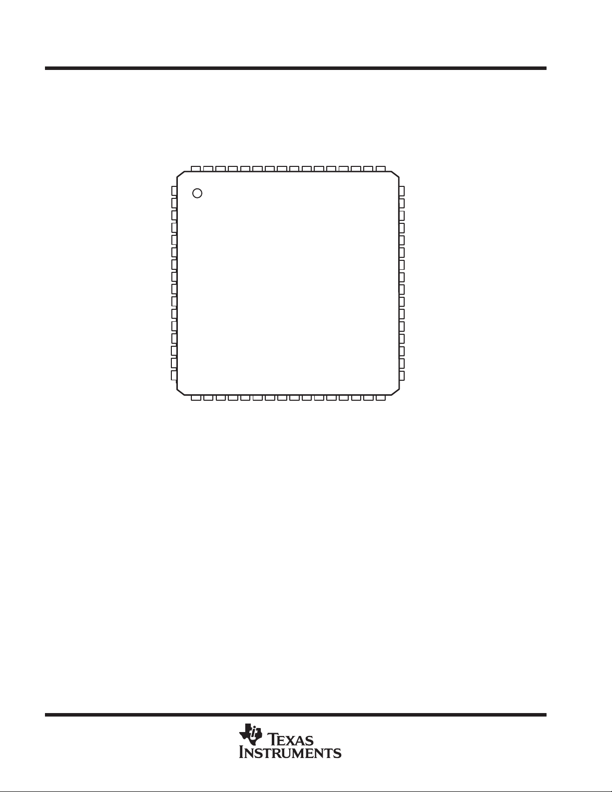
pin assignments
PAP PACKAGE
(TOP VIEW)
NC
OUT3
63 62 61 60 5964 58 56 55 5457
1
NC
OUT4
GNDLED
OUT5
OUT6
GNDLED
OUT7
OUT8
GNDLED
OUT9
OUT10
GNDLED
OUT11
NC
NC
NC
2
3
4
5
6
7
8
9
10
11
12
13
14
15
16
17 18
19
NC
OUT12
NC – No internal connection
GNDLED
OUT2
OUT1
21 22 23 24
20
OUT13
OUT14
GNDLED
GNDLED
OUT0NCNC
NC
OUT15
GNDLED
BCENA
GNDLOG
MODEVTSENANCSIN
53 52 51 50 49
25 26 27 28 29
IREF
CCLED
WDCAP
V
GNDANA
CCLOG
30 31 32
NC
CCANA
V
48
47
46
45
44
43
42
41
40
39
38
37
36
35
34
33
SOUT
MCENA
TEST2
SOMODE
GSCLK
BLANK
RSEL1
RSEL0
SCLK
XENABLE
XOE
WDTRG
XLATCH
XDOWN1
XDOWN2
TEST1
BOUT
GSOUT
2
POST OFFICE BOX 655303 • DALLAS, TEXAS 75265
Page 3
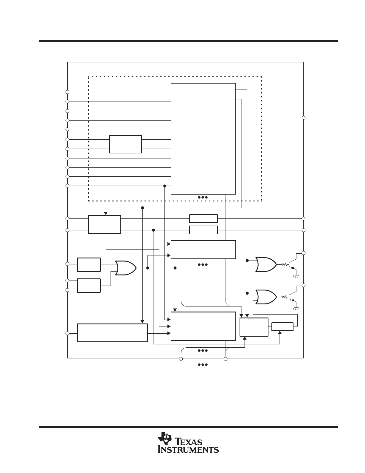
functional block diagram
TLC5905
LED DRIVER
SLLS401 – NOVEMBER 1999
Shift Register and Data Latch
MCENA
BCENA
RSEL0
RSEL1
SIN
XENABLE
SCLK
SOMODE
XOE
XLATCH
MODE
GSCLK
BLANK
TSENA
Gray Scale
TSD
8 bits
Counter
SCLK
Controller
OVM
Shift Register
Data Latch
Brightness Control
Shift Register
Data Latch
Gray Scale Control
Shift Register
Data Latch
DELEY
DELEY BOUT
16 x 8 bits
Comparator
SOUT
GSOUT
XDOWN1
WDTRG
WDCAP
IREF
NOTE: All the input terminals are with Schmitt-triggered inverter except IREF and WDCAP.
WDT
Current Reference
Circuit
Constant Current Driver
16 bits
OUT0 OUT15
16 bits
OVM Comp
XDOWN2
LATCH
POST OFFICE BOX 655303 • DALLAS, TEXAS 75265
3
Page 4
TLC5905
LED DRIVER
SLLS401 – NOVEMBER 1999
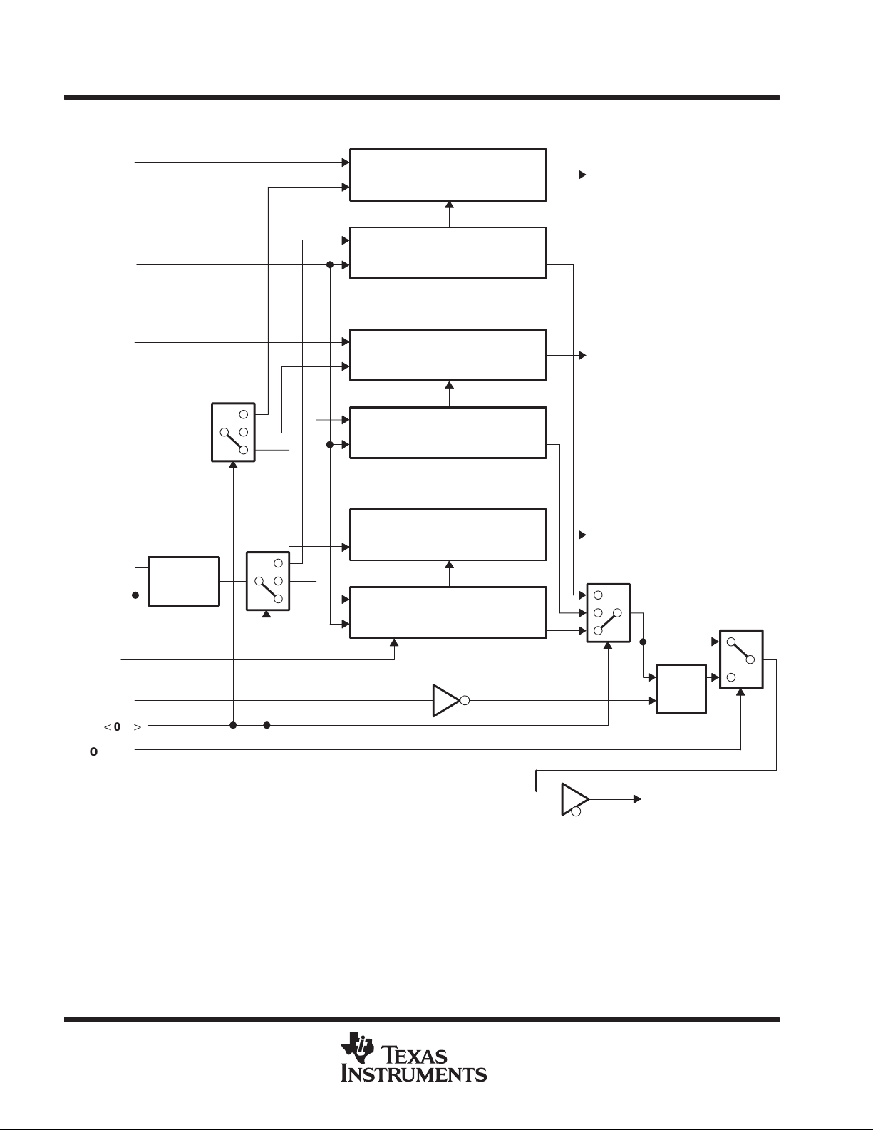
functional block diagram for shift register and data latch
MCENA
SIN
BCENA
XLATCH
XENABLE
SCLK
SCLK
Controller
OVM Data Latch
(1 x 8 bit)
OVM Shift Register
(8 x 1 bit)
Brightness Control Data Latch
(1 x 8 bit)
Brightness Control Shift Register
(8 x 1 bit)
Gray Scale Control Data Latch
(16 x 8 bit)
Gray Scale Control Shift Register
(128 x 1 bit / 64 x 1 bit)
16 bit OVM Comparator
XDOWN1, 2 Output Driver
Constant Current Driver Control
Gray Scale Clock Counter
16 x 8 bit Data Comparator
MODE
RSELt0–1
SOMODE
NOTE: Enclosed in ( ) is dependent on MODE pin selection.
u
XOE
(see Note)
1 bit
S/R
SOUT
4
POST OFFICE BOX 655303 • DALLAS, TEXAS 75265
Page 5
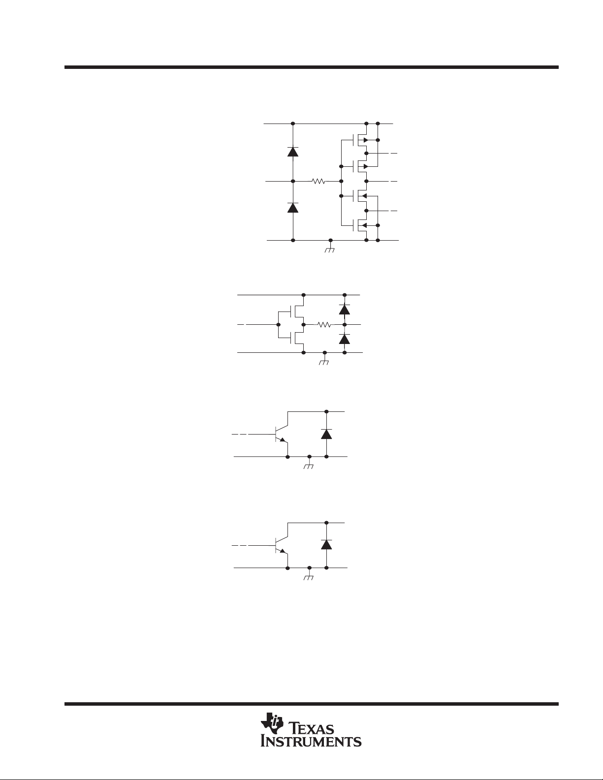
equivalent input and output schematic diagrams
TLC5905
LED DRIVER
SLLS401 – NOVEMBER 1999
Input
SOUT, GSOUT, BOUT
XDOWN1, XDOWN2
VCCLOG
INPUT
GNDLOG
VCCLOG
OUTPUT
GNDLOG
OUTn
XDOWN1, XDOWN2
GNDLOG
OUTn
GNDLED
POST OFFICE BOX 655303 • DALLAS, TEXAS 75265
5
Page 6
TLC5905
I/O
DESCRIPTION
Á
Á
Á
Á
Á
Á
Á
Á
Á
Á
Á
Á
Á
Á
Á
Á
Á
Á
Á
Á
Á
Á
Á
Á
Á
Á
Á
Á
Á
Á
Á
Á
Á
Á
Á
Á
Á
Á
Á
Á
Á
Á
Á
Á
Á
Á
Á
Á
Á
Á
Á
Á
Á
Á
Á
Á
Á
Á
Á
Á
Á
Á
Á
LED DRIVER
SLLS401 – NOVEMBER 1999
TERMINAL
NAME NO.
ÁÁÁÁ
BCENA
ÁÁÁÁ
ÁÁÁÁ
BLANK
BOUT
GSCLK
ÁÁÁÁ
GNDANA
GNDLED
GNDLOG
GSOUT
IREF
ÁÁÁÁ
MCENA
ÁÁÁÁ
MODE
NC
ÁÁÁÁ
OUT0 – OUT15
ÁÁÁÁ
ÁÁÁÁ
RSEL0
RSEL1
ÁÁÁÁ
ÁÁÁÁ
SCLK
ÁÁÁÁ
ÁÁÁÁ
SIN
SOMODE
ÁÁÁÁ
SOUT
ÁÁÁÁ
TEST1
TEST2
THERMAL PAD
TSENA
ÁÁÁÁ
ÁÁÁÁ
ÁÁÁÁ
ÁÁÁÁ
ÁÁÁÁ
ÁÁÁÁ
ÁÁÁÁ
1,7,10,16,17,24,
ÁÁÁÁ
29,50,56,57,64
2,4,5,8,9,12,13
ÁÁÁÁ
15,18,20,21,23
ÁÁÁÁ
ÁÁÁÁ
ÁÁÁÁ
ÁÁÁÁ
ÁÁÁÁ
ÁÁÁÁ
ÁÁÁÁ
package bottom
ÁÁÁÁ
55
45
34
46
28
3,6,11,14,
19,22,59,62
54
33
25
31
53
58,60,61,63,
43
44
42
49
47
32
35
48
51
Terminal Functions
Brightness control enable. When BCENA is low, the brightness control latch is set to the
Á
Á
Á
Á
I/O
Á
Á
ÁÁББББББББББББББББББББ
Á
Á
Á
Á
Á
Á
Á
Á
Á
ББББББББББББББББББББ
default value. The output current value in this status is 100% of the value set by an external
I
resistor. The frequency division ratio of GSCLK is1/1. When BCENA is high, writing to
ББББББББББББББББББББ
brightness control latch is enabled.
Blank(Light off). When BLANK is high, all the output of the constant current driver is turned
ББББББББББББББББББББ
off. The constant current output is turned on (LED on) when synchronized to the falling edge
I
of GCLK after next rising edge of GCLK when BLANK goes from high to low.
O
Blank signal delay. BOUT is an output with the addition of delay time to BLANK.
Clock input for gray scale. The gray scale display is accomplished by lighting the LED on until
I
ББББББББББББББББББББ
the number of GSCLK counted is equal to data latched.
Analog ground (internally connected to GNDLOG and GNDLED)
LED driver ground (internally connected to GNDANA and GNDLOG)
Logic ground (internally connected to GNDANA and GNDLED)
O
Clock delay for gray scale. GSOUT is an output with the addition of delay time to GSCLK.
Constant current value setting. LED current is set to the desired value by connecting an
external resistor between IREF and GND. The 37 times current is compared to current across
ББББББББББББББББББББ
the external resistor sink on the output terminal.
OVM enable. When MCENA is low, the OVM latch is set to the default value. The comparison
I
ББББББББББББББББББББ
voltage in this status is 0.3 V. When MCENA is high, writing to OVM latch is enabled.
8/16 bits select. When MODE is high, the 16 bits output is selected. When MODE is low, the
I
8 bits output is selected.
No internal connection
O
Constant current output
ББББББББББББББББББББ
Shift register data latch switching.
ББББББББББББББББББББ
When RSEL1 is low and RESL0 is low, gray scale data shift register latch is selected.
When RSEL1 is low and RESL0 is high, the brightness control register latch is selected.
I
ББББББББББББББББББББ
When RSEL1 is high and RSEL0 is low, the OVM register latch is selected.
When RSEL1 is high and RSEL0 high, no register latch is selected.
ББББББББББББББББББББ
Clock input for data transfer. The input data is from SIN. All data on the shift register selected
by RSEL0 and RSEL1, and output data at SOUT are sifted by 1 bit synchronizing to SCLK.
I
ББББББББББББББББББББ
The data except the SOUT is synchronized to the rising edge. The edge for data from SOUT
is determined by the level of SOMODE.
ББББББББББББББББББББ
Input for 1 bit serial data. These terminals are inputs for shift register for gray scale data,
I
brightness control and OVM. The register selected is determined by RSEL0, 1.
Timing select for data output. When SOMODE is low , SOUT is changed by synchronizing to
the rising edge of SCLK. When SOMODE is high, SOUT is changed by synchronizing to the
I
ББББББББББББББББББББ
falling edge of SCLK.
Output for 1 bit serial data with 3–state. These terminals are outputs for shift register for gray
O
ББББББББББББББББББББ
scale data, brightness control and OVM. The register selected is determined by RSEL0, 1.
TEST. Factory test terminal. TEST1 and TEST2 should be connected to GND for normal
I
operation.
Heat sink pad. This pad is connected to the lowest potential IC or thermal layer.
TSD (thermal shutdown) enable. When TSENA is high, TSD is enabled. When TSENA is low,
I
ББББББББББББББББББББ
TSD is disabled.
6
POST OFFICE BOX 655303 • DALLAS, TEXAS 75265
Page 7
I/O
DESCRIPTION
Á
Á
Á
Á
Á
Á
Á
Á
Á
Á
Á
Á
Á
Á
Á
Á
Á
Á
Á
Á
Á
Á
Á
Á
TERMINAL
NAME NO.
V
CCANA
V
CCLOG
V
CCLED
ÁÁÁÁ
WDCAP
ÁÁÁÁ
WDTRG
ÁÁÁÁ
XDOWN1
ÁÁÁÁ
XDOWN2
ÁÁÁÁ
XENABLE
ÁÁÁÁ
XLATCH
ÁÁÁÁ
XOE
ÁÁÁÁ
30
52
26
ÁÁÁÁ
27
ÁÁÁÁ
39
ÁÁÁÁ
37
ÁÁÁÁ
36
ÁÁÁÁ
41
ÁÁÁÁ
38
ÁÁÁÁ
40
ÁÁÁÁ
LED DRIVER
SLLS401 – NOVEMBER 1999
Terminal Functions (Continued)
Analog power supply voltage
Logic power supply voltage
LED driver power supply voltage
WDT (watchdog timer) detection time adjustment. WDT detection time is adjusted by
connecting a capacitor between WDCAP and GND. When WDCAP is directly connected
ББББББББББББББББББББ
I
to GND, the WDT function is disabled. In this case, WDTRG should be tied to a high or low
ББББББББББББББББББББ
level.
WDT (watchdog timer) trigger input. By applying a scan signal to this terminal, the scan
signal can be monitored by turning the constant current output off and protecting the LED
I
ББББББББББББББББББББ
from damage by burning when the scan signal is stopped during constant period designed.
Shutdown. XDOWN1 is configured as an open collector. It goes low when constant current
O
output is shut down by the WDT or TSD function.
ББББББББББББББББББББ
OVM comparator output. XDOWN2 is configured as open collector. It monitors terminal
voltage when constant current output is turned on. XDOWN2 goes low when this voltage is
O
ББББББББББББББББББББ
lower than the level selected by the OVM latch. When BLANK is set high, the previous level
is held.
SCLK enable. When XENABLE is low, data transfer is enabled. Data transfer starts on the
I
ББББББББББББББББББББ
rising edge of SCLK after XENABLE goes low. During XENABLE high, no data is transferred.
Latch. When XLATCH is high, data on shift register goes through latch. When XLATCH is
low, data is latched. Accordingly, if data on shift register is changed during XLATCH high,
I
ББББББББББББББББББББ
this new value is latched (level latch).
Data output enable. When XOE is low, the SOUT terminal is drived. When XOE is high, the
I
ББББББББББББББББББББ
SOUT terminal goes to high-impedance state.
TLC5905
absolute maximum ratings over operating free-air temperature (unless otherwise noted)
Logic supply voltage, V
CC(LOG)
Supply voltage for constant current circuit, V
Analog supply voltage, V
Output current (DC), I
CC(ANA)
OL(C)
Input voltage range, VI – 0.3 V to V
Output voltage range, V
Output voltage range, V
(SOUT)
(OUTn)
Storage temperature range, T
– 0.3 V to 7 V. . . . . . . . . . . . . . . . . . . . . . . . . . . . . . . . . . . . . . . . . . . . . . . . . . . . .
CC(LED)
– 0.3 V to 7 V. . . . . . . . . . . . . . . . . . . . . . . . . . . . . . . . . . .
– 0.3 V to 7 V. . . . . . . . . . . . . . . . . . . . . . . . . . . . . . . . . . . . . . . . . . . . . . . . . . . .
90 mA. . . . . . . . . . . . . . . . . . . . . . . . . . . . . . . . . . . . . . . . . . . . . . . . . . . . . . . . . . . . . . .
, V
(BOUT)
and V
–40°C to 125°C. . . . . . . . . . . . . . . . . . . . . . . . . . . . . . . . . . . . . . . . . . . . . . . . . . .
stg
and V
(XDOWNn)
(GSOUT)
– 0.3 V to V
– 0.3 V to 18 V. . . . . . . . . . . . . . . . . . . . . . . . . . . . . . . . . . . . . . .
CC(LOG)
CC(LOG)
†
+ 0.3 V. . . . . . . . . . . . . . . . . . . . . . . . . . . . . . . . . . . . . . . . . . . . . . . . .
+ 0.3 V. . . . . . . . . . . . . . . . . . .
Continuous total power dissipation at (or below) TA = 25°C 4.9 W. . . . . . . . . . . . . . . . . . . . . . . . . . . . . . . . . . . . .
Power dissipation rating at (or above) TA = 25°C 39.4 mW/°C. . . . . . . . . . . . . . . . . . . . . . . . . . . . . . . . . . . . . . .
†
Stresses beyond those listed under “absolute maximum ratings” may cause permanent damage to the device. These are stress ratings only, and
functional operation of the device at these or any other conditions beyond those indicated under “recommended operating conditions” is not
implied. Exposure to absolute-maximum-rated conditions for extended periods may affect device reliability.
NOTE 1: All voltage values are with respect to GNDLOG terminal.
POST OFFICE BOX 655303 • DALLAS, TEXAS 75265
7
Page 8
TLC5905
Á
Á
Á
Á
Á
Á
Á
Á
Á
Á
Á
Á
Á
Á
Á
Á
Á
Á
Á
Á
Á
mA
Low-level output current, I
SCLK clock frequenc
f
MH
GSCLK clock frequenc
f(
MH
GSCLK pulse duration (high or low level), t
ns
LED DRIVER
SLLS401 – NOVEMBER 1999
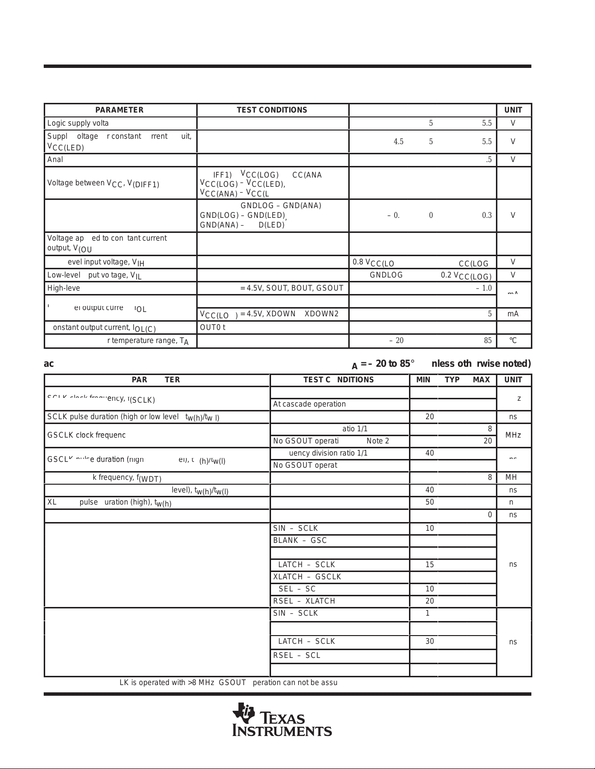
recommended operating conditions
dc characteristics
PARAMETER
Logic supply voltage, V
Supply voltage for constant current circuit,
ББББББББББ
V
CC(LED)
Analog power supply, V
Voltage between VCC, V
ББББББББББ
Voltage between GND, V
ББББББББББ
Voltage applied to constant current
output, V
ББББББББББ
(OUTn)
High-level input voltage, V
Low-level input voltage, V
High-level output current, I
p
Constant output current, I
Operating free–air temperature range, T
CC(LOG)
CC(ANA)
(DIFF1)
(DIFF2)
IH
IL
OH
OL
OL(C)
БББББББББÁÁÁÁ
V
(DIFF1)
V
CC(LOG)
БББББББББ
V
CC(ANA)
V
(DIFF2)
GND(LOG) – GND(LED),
БББББББББ
GND(ANA) – GND(LED)
OUT0 to OUT15 off
БББББББББ
V
CC(LOG)
V
CC(LOG)
V
CC(LOG)
OUT0 to OUT15
A
TEST CONDITIONS
= V
– V
– V
CC(LOG)
CC(LED),
CC(LED)
– V
CC(ANA)
= GNDLOG – GND(ANA)
= 4.5V, SOUT, BOUT, GSOUT
= 4.5V, SOUT, BOUT, GSOUT
= 4.5V, XDOWN1, XDOWN2
MIN
ÁÁÁ
ÁÁÁ
ÁÁÁÁÁÁÁÁÁ
0.8 V
CC(LOG)
GNDLOG
4.5
4.5
4.5
– 0.3
– 0.3
NOM
Á
Á
Á
5
5
ÁÁÁ
5
0
ÁÁÁ
0
ÁÁÁ
0.2 V
MAX
V
CC(LOG)
CC(LOG)
5
– 20
5.5
5.5
5.5
0.3
0.3
17
– 1.0
1.0
80
85
UNIT
V
V
Á
V
V
Á
V
Á
V
Á
V
V
5
mA
mA
°C
ac characteristics, V
CC(LOG)
PARAMETER
y,
(SCLK)
SCLK pulse duration (high or low level), t
y,
GSCLK)
p
WDTRG clock frequency, f
(WDT)
WDTRG pulse duration (high or low level), t
XLATCH pulse duration (high), t
Rise/fall time, tr/t
f
w(h)
= V
CC(ANA)
w(h)/tw(l)
w(h)/tw(l)
w(h)/tw(l)
= V
CC(LED)
= 4. 5 V to 5 . 5 V, T
TEST CONDITIONS
At single operation
At cascade operation (SOMODE = L)
Frequency division ratio 1/1
No GSOUT operation (see Note 2)
Frequency division ratio 1/1
No GSOUT operation (see Note 2)
SIN – SCLK
BLANK – GSCLK
XENABLE – SCLK
Setup time, t
su
XLATCH – SCLK
XLATCH – GSCLK
RSEL – SCLK
RSEL – XLATCH
SIN – SCLK
XENABLE – SCLK
Hold time, t
h
XLATCH – SCLK
RSEL – SCLK
RSEL – XLATCH
NOTE 2: When GSCLK is operated with >8 MHz, GSOUT operation can not be assured.
= – 20 to 85°C (u n l e s s o t h e r w i s e n o t e d)
A
MIN
TYP
MAX
UNIT
15
10
20
8
20
40
20
8
MHz
40
50
100
10
20
15
15
10
10
20
10
20
30
20
20
z
ns
z
ns
ns
ns
ns
ns
8
POST OFFICE BOX 655303 • DALLAS, TEXAS 75265
Page 9
Á
Á
Á
Á
Á
VOLLow-level output voltage
V
Á
Á
Á
Á
Á
(LOG)
y(g)
I
Supply current (analog)
mA
Á
Á
Á
Á
Á
Á
Á
Á
Á
Á
Á
Á
Á
()
Á
Á
Á
Á
Á
Á
Á
Á
Á
Á
Á
Á
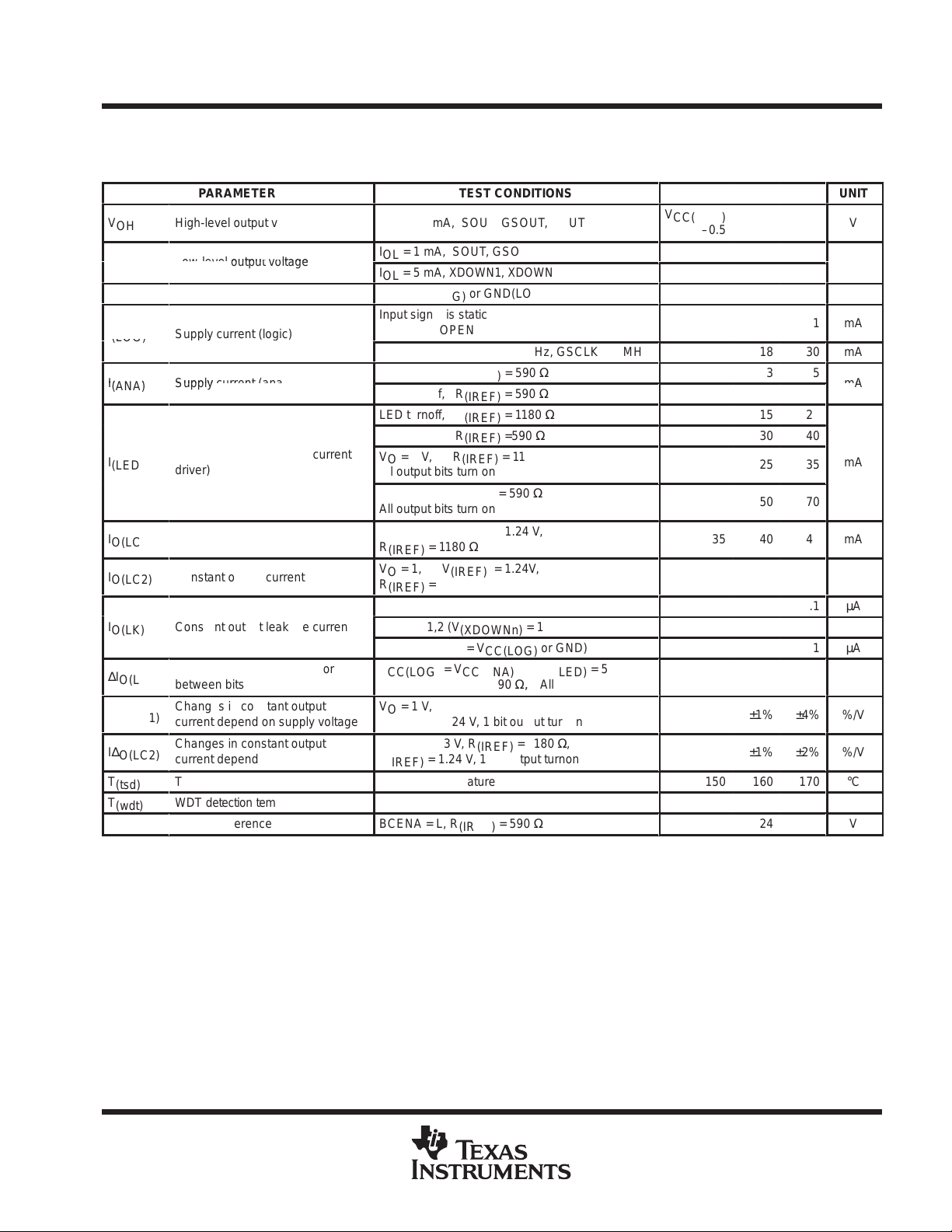
electrical characteristics,
= V
p
= V
CC(ANA)
CC(ANA)
MIN/MAX:V
TYP: V
V
I
I
I
I
I
I
∆I
I∆
I∆
T
T
V
OH
ÁÁ
I
ÁÁ
(ANA)
(LED)
ÁÁ
O(LC1)
ÁÁ
O(LC2)
O(LK)
O(LC)
ÁÁ
O(LC1)
O(LC2)
ÁÁ
(tsd)
(wdt)
(IREF)
CC(LOG)
High-level output voltage
Input current
Supply current (logic)
Supply current (constant current
driver)
Constant output current
Constant output current
Constant output leakage current
Constant output current error
between bits
Changes in constant output
current depend on supply voltage
Changes in constant output
current depend on output voltage
TSD detection temperature
WDT detection temperature
Voltage reference
CC(LOG)
PARAMETER
БББББББ
БББББББ
pp
БББББББ
БББББББ
БББББББ
БББББББ
= V
= V
= 4.5 V to 5.5 V, T
CC(LED)
CC(LED)
A
= 5 V, TA = 25°C (unless otherwise noted)
TEST CONDITIONS
IOH = –1 mA, SOUT, GSOUT, BOUT
БББББББББББ
IOL = 1 mA, SOUT, GSOUT, BOUT
IOL = 5 mA, XDOWN1, XDOWN2
VI = V
CC(LOG)
or GND(LOG)
Input signal is static, TSENA = H,
БББББББББББ
WDCAP = OPEN
Data transfer, SCLK = 15 MHz, GSCLK = 8 MHz
LED turnon, R
LED turnoff, R
LED turnoff, R
LED turnoff, R
VO = 1 V, R
All output bits turn on
БББББББББББ
VO = 1 V, R
All output bits turn on
VO = 1 V, V
БББББББББББ
R
(IREF)
VO = 1, V
R
(IREF)
(IREF)
= 1180 Ω
(IREF)
= 590 Ω
OUT0 to OUT15 (V
XDOWN1,2 (V
SOUT (V
V
VO = 1V , R
БББББББББББ
VO = 1 V, R
V
OUTn
CC(LOG)
= V
(IREF)
(IREF)
= 1.24 V, 1 bit output turnon
(IREF)
VO= 1 V to 3 V, R
БББББББББББ
V
= 1.24 V, 1 bit output turnon
(IREF)
= 590 Ω
(IREF)
= 590 Ω
(IREF)
= 1180 Ω
(IREF)
=590 Ω
(IREF)
= 1180 Ω
(IREF)
= 590 Ω
(IREF)
= 1.24 V,
= 1.24V,
= 15 V)
(OUTn)
(XDOWNn)
= V
CC(ANA)
= 15 V)
= V
or GND)
CC(LED)
CC(LOG)
= 590 Ω, All output bits turnon
= 1180 Ω,
= 1180 Ω,
(IREF)
Junction temperature
No external capacitor
BCENA = L, R
(IREF)
= 590 Ω
= –20 to 85°C
= 5 V,
LED DRIVER
SLLS401 – NOVEMBER 1999
MIN
V
CC(LOG)
ÁÁ
ÁÁÁÁÁÁ
ÁÁÁÁ
ÁÁ
ÁÁÁÁ
ÁÁÁÁ
TYP
–0.5
ÁÁÁÁÁ
18
3
3
15
30
25
50
35
70
Á
40
80
±1%
±1%
±1%
150
160
5
10
1.24
MAX
Á
Á
Á
Á
TLC5905
UNIT
0.5
0.5
±1
1
Á
30
5
5
20
40
35
Á
70
45
Á
90
0.1
1
1
±4%
Á
±4%
±2%
170
15
%/V
%/V
Á
V
µA
mA
mA
mA
mA
mA
µA
µA
µA
°C
ms
V
POST OFFICE BOX 655303 • DALLAS, TEXAS 75265
9
Page 10

TLC5905
LED DRIVER
SLLS401 – NOVEMBER 1999
switching characteristics, CL = 15pF,
MIN/MAX: V
TYP: V
trRise time
tfFall time
tdPropagation delay time
NOTE 3: Until SOUT will be turned on (drive) or turned off (Hi–Z).
CC(LOG)
CC(LOG)
= V
= V
CC(ANA)
PARAMETER
CC(ANA)
= V
= V
CC(LED)
CC(LED)
= 4.5 V to 5.5 V, T
= 5 V, T
= –20 to 85°C
= 25°C (unless otherwise noted)
A
TEST CONDITIONS
SOUT
GSOUT, BOUT
OUTn (see Figure 1)
SOUT
GSOUT, BOUT
OUTn (see Figure 1)
OUTn+1 – OUTn
BLANK↑ – OUT0
BLANK – BOUT
GSCLK↓ – OUT0
GSCLK – GSOUT
SCLK – SOUT
XOE↓ – SOUT (see Note 3)
XOE↑ – SOUT (see Note 3)
GSCLK – XDOWN2
A
MIN
20
20
15
10
10
TYP
250
200
350
350
12
13
10
35
40
40
30
20
15
MAX
8
5000
30
30
20
25
60
500
70
500
70
50
35
25
UNIT
ns
ns
ns
10
POST OFFICE BOX 655303 • DALLAS, TEXAS 75265
Page 11

TLC5905
LED DRIVER
SLLS401 – NOVEMBER 1999
PARAMETER MEASUREMENT INFORMATION
V
CC
90%
10%
100%
50%
0%
V
CC
IREF OUTn
590 Ω
GND
Figure 1. Rise Time and Fall Time Test Circuit for OUTn
V
IH
V
t
r
t
w(h)
t
f
t
IL
w(l)
100%
50%
0%
V
IH
V
IL
100%
50%
51 Ω
15 pF
0%
VIH or V
VIL or V
t
d
OH
OL
VIH or V
VIL or V
OH
OL
Figure 2. Timing Requirements
POST OFFICE BOX 655303 • DALLAS, TEXAS 75265
11
Page 12

TLC5905
LED DRIVER
SLLS401 – NOVEMBER 1999
PRINCIPLES OF OPERATION
constant current output selection by user (80 mA x16 bits or 120 mA x 8 bits)
When the MODE terminal is set to high, output is selected as 80 mA x 16 bits. When the MODE terminal is set
to low, output is selected as 120 mA x 8 bits. By this setting, the shift register latch for gray scale data is changed
to the configuration corresponding to the bit selected. Note that two constant output terminals should be tied
to LED such as OUT0-to-OUT1 and OUT2-to-OUT3 because they operate in pairs when the 8-bit output mode
is selected. Also, in this case, the current value on constant current output is the same as in 16-bit output mode.
Therefore, when output current of 120 mA is desired, the resister connected to the IREF terminal should be set
to the same value as the output current of 60 mA.
Table 1. Operation Mode Selection
MODE
H
L
80 mA × 16 bits
120 mA × 8 bits
OUTPUT
On the constant current output terminals (OUT0–15), approximately 37 times the current that flows through
external resistor, R
(connected between IREF and GND), can flow. The external resistor value is calculated
IREF
using the following equation.
R
(Ω) ≅ 37 × 1.24 (V) / I
(IREF)
(A) where BCENA is low.
OL(C)
Note that more current flows if IREF is connected directly to GND.
constant output current operation
The constant current output turns on (sink constant current), if all the gray scale data latched into the gray scale
latch is not zero on the falling edge of the gray scale clock after the next rising edge of the gray scale clock when
BLANK goes from high to low . After that, the number of the falling edge is counted by the 8-bit gray scale counter.
Then, output counted corresponding to the gray scale data is turned off (stop to sink constant current). If the
shift register for gray scale is updated during XLA TCH high, data on the gray scale data latch is also updated
affecting the number of the gray scale of constant current output. Accordingly, during on-state of constant
current output, XLA TCH should be kept at a low level and the gray scale data latch should be held. If there are
constant current output terminals unconnected (includes LED disconnection), the LED should be turned on after
writing zero to the gray scale data latch corresponding to the output unconnected. Unless this action is taken,
supply current on the constant current driver will increase resulting in influencing the current value for the
constant current output when turned on.
shift register latch
The device provides three kinds of shift register latchs including the gray scale data, brightness control, and
OVM. To write data into the shift register, SCLK and SIN are utilized. The selection of the shift register will be
done by RSEL0 and RSEL1 as shown in Table 2. Note that RSEL0 and RSEL1 should be changed when both
SCLK and XLATCH are low.
Table 2. Shift Register Latch Selection
RSEL0
L
L
H
H
12
RSEL1
L
H
L
H
POST OFFICE BOX 655303 • DALLAS, TEXAS 75265
SHIFT REGISTER LATCH SELECTED
Shift register latch for gray scale data
Shift register latch for brightness control
Shift register latch for OVM
N/A (SOUT is tied to low level)
Page 13

LED DRIVER
SLLS401 – NOVEMBER 1999
PRINCIPLES OF OPERATION
shift register latch for gray scale data
The shift register latch for gray scale data is set as a 64 x 1 bit configuration in the 8-bit mode, and as a 128
x 1 bit configuration in the 16-bit mode. The gray scale data, configured as 8 bits, represents the time when
constant current output is being turned on, and the data range is 0 to 255 (00h to FFh). When the gray scale
data is 0, the time is shortest, and the output is not turned on(light off). On the other hand, when the gray scale
data is 255, the time is longest, and it turns on during time of 255 clocks from GSCLK. The configuration of shift
register and latch for gray scale data is shown in Figure 3.
Latch for Gray Scale Data
TLC5905
XLATCH
SOUT
XLATCH
SOUT
OUT15 Data
(8 bits)
Shift Register for Gray Scale Data
MSB
128 121
Latch for Gray Scale Data
OUT15,14 Data
(8 bits)
Shift Register for Gray Scale Data
MSB
64 57
OUT14 Data
(8 bits)
120 113 16 9
16 Bit Mode (MODE=H, RSEL0 and RSEL1=L)
OUT13,12 Data
(8 bits)
56 49 16 9
8 Bit Mode (MODE=L, RSEL0 and RSEL1=L)
. . . . . . . . . .
. . . . . . . . . .
. . . . . . . . . .
. . . . . . . . . .
OUT1 Data
(8 bits)
OUT3,2 Data
(8 bits)
OUT0 Data
(8 bits)
LSB
8 0
OUT1,0 Data
(8 bits)
LSB
8 0
SCLK
SIN
SCLK
SIN
Figure 3. Relationship Between Shift Register and Latch for Gray Scale Data
POST OFFICE BOX 655303 • DALLAS, TEXAS 75265
13
Page 14

TLC5905
LED DRIVER
SLLS401 – NOVEMBER 1999
PRINCIPLES OF OPERATION
shift register latch for brightness control and OVM
The shift register latch for both the brightness control and OVM (output voltage monitor) is configured with a
1 x 1 byte. In the shift register latch for brightness control, the division ratio of GSCLK can be set and the output
current value on constant current output can be adjusted. In the shift register latch for OVM, the comparison
voltage at the OVM comparator on constant current output terminals (OUT0 to OUT15) can be set and the output
signal for both XDOWN1 and XDOWN2 can be forced to a low level. When powered up, the latch data is
indeterminate and shift register is not initialized. When these functions are used, data should be written to the
shift register latch prior to turning the constant current output on (BLANK=L). Also, it is inhibited from rewriting
the latch value for brightness control when the constant current output is turned on. When these functions are
not used, latch value can be set to the default value setting of BCENA or MCENA or to low level (tied to GND).
The configuration of the shift register and latch for brightness control and monitor control is shown in Figure 4.
Latch for Brightness Control
GSCLK Division Ratio Data Set Current Data Adj usted On Con stant Curr ent O utput
GSCLK Division Ratio Data Set
XLATCH
00011111
MSB LSB MSB LSB
(see Note)
Shift Register for Brightness Control
SOUT
XLATCH
SOUT
NOTE: Indicates default value at BCENA low if brightness control latch, at MCENA low if OVM latch.
8th bit
Latch for OVM
Shift Register for OVM
8th bit 7th bit 6th bit 5th bit 4th bit 3rd bit 2nd bit 1st bit
7th bit 6th bit 5th bit 4th bit 3rd bit 2nd bit 1st bit
Monitor Control Data
N/A
0001
MSB LSB
Figure 4. Relationship Between Shift Register and Latch for Brightness Control and OVM
write data to shift register latch
The shift register latch written is selected using the RSEL0 and RSEL1 terminal. The data is applied to the SIN
data input terminal and clocked into the shift register synchronizing to the rising edge of SCLK after XENABLE
is pulled low. The shift register for gray scale data is 64 bit length in the 8 bit mode resulting in 64 times of SCLK,
and 128 bit length in the16 bit mode resulting in 128 times of SCLK. Brigtness control and monitor control results
in eight times the SCLK input. At number of SCLK input for each case, data can be written into the shift register.
In this condition, when XLA TCH is pulled high, data in the shift register is clocked into latch (data through), and
when XLATCH is pulled low, data is held (latch).
SCLK
SIN
(see Note)
SCLK
SIN
14
POST OFFICE BOX 655303 • DALLAS, TEXAS 75265
Page 15

Á
Á
Á
Á
Á
Á
Á
Á
Á
Á
Á
Á
Á
Á
Á
Á
Á
Á
Á
LED DRIVER
SLLS401 – NOVEMBER 1999
PRINCIPLES OF OPERATION
brightness control function
By writing data into the brightness control latch, current on all constant current outputs can be adjusted to control
the variation of brightness between ICs and the division ratio for the gray scale clock can be set to control the
variation of brightness for the total panel system.
output current adjustment on all constant current outputs – brightness adjustment between ICs
By using the lower 5 bits of the brightness control latch, output current can be adjusted to 32 steps as 1 step
of 1.6% current ratio between 100% and 51.6% when the output current is set to 100% of an external resistor.
By using this function, the brightness control between modules (ICs) can be adjusted, sending the desired data
externally even if ICs are mounted on a print-circuit board. When BCENA is pulled low, the output current is set
to 100%.
Table 3. Relative Current Ratio For Total Constant Current Output
TLC5905
CODE
MSB 00000 LSB
.
.
ÁÁÁÁ
.
.
ÁÁÁÁ
11110
11111
†
BCENA is low.
†
CURRENT RATIO%
51.6
.
БББББ
БББББ
.
.
.
98.4
100
20 (mA)
10.3
.
.
ÁÁ
.
.
ÁÁ
19.3
20.0
80 (mA)
41.3
.
.
ÁÁ
.
.
ÁÁ
78.7
80.0
V
(TYP)
IREF
0.63
.
.
ÁÁÁ
.
.
ÁÁÁ
1.22
1.24
frequency division ratio setting for gray scale clock – panel brightness adjustment
By using the upper 3 bits of the brightness control latch, the gray scale clock can be divided into 1/1 to 1/8. If
the gray scale clock is set to 8 times the speed (256 × 8 = 2048) of frequency during horizontal scanning time,
the brightness can be adjusted to 8 steps by selecting the frequency division ratio. Therefore, the total panel
brightness can be adjusted at once, and applied to the brightness of day or night. When BCENA is pulled low,
the gray scale clock is not divided. When BCENA is pulled high, the brightness can be adjusted as shown in
Table 4.
Table 4. Relative Brightness Ratio For Total Constant Current Output
CODE
ÁÁÁÁ
MSB 000 LSB
ÁÁÁÁ
ÁÁÁÁ
.
.
.
.
110
111
†
BCENA is low.
FREQUENCY
DIVISION RATIO
БББББ
†
БББББ
БББББ
1/1
.
.
.
.
1/7
1/8
RELATIVE BRIGHTNESS RATIO
ББББББББ
(%)
12.5
ББББББББ
ББББББББ
.
.
.
.
87.5
100
OVM (output voltage monitor) function
By writing data into the OVM latch, the comparison voltage for voltage comparator of OUT0 to OUT15 can be
set and the output signal for XDOWN1 and XDOWN2 can be checked.
POST OFFICE BOX 655303 • DALLAS, TEXAS 75265
15
Page 16

TLC5905
LED DRIVER
SLLS401 – NOVEMBER 1999
PRINCIPLES OF OPERATION
OVM (output voltage monitor) function (continued)
OVM comparator
The OVM comparator compares the voltage on the constant current output terminal during turnon with
comparison voltage set by the OVM latch. When the voltage on the constant current output terminal is lower,
XDOWN2 goes low. As shown in Figure 5, the comparator is provided in every output portion, and the
comparison result corresponding to the output to be turned on appears in the XDOWN2 terminal. Since the
XDOWN2 terminal is an open-collector output, outputs of multiple ICs are brought together.
The output terminal for comparison result is XDOWN2 only . The voltage on all the constant current output can
be checked to monitor XDOWN2, turning output on in turn. The voltage on the constant current output, when
turned on, can also be measured, resulting in a change to the comparison voltage set by the OVM latch. Using
this function, the sensing (LOD function) LED disconnection (output voltage is below 0.3 V) and short circuit
(output voltage is extremely high) can be detected and specifies which LED has encountered this failure. Also,
by monitoring the output voltage and controlling the voltage across anode of the LED to minimize the voltage
on the constant current output (approximately 0.7 V at I
minimized. Furthermore, by setting BLANK to low during LED on, the previous comparison result can be held.
Thus, synchronizing timing to check XDOWN2 from the system to the LED lighting timing is not required. Note
that the gray scale data being turned on should be a minimum of 5 µs since the XDOWN2 output is required
approximately 5 µs after the constant current output is turned on. The comparison result is also required
approximately 5 µs after latch data is changed.
= 80 mA), the rising temperature of the chip can be
O
OUT0
Internal OUT0
Turn ON Signal
OUT1
Internal OUT1
Turn ON Signal
OUT14
Internal OUT014
Turn ON Signal
OUT15
Internal OUT015
Turn ON Signal
–
+
–
+
–
+
–
+
Comparison Voltage
XDOWN2
D
Q
LATCH
BLANK
When BLANK is high, hold the data
When BLANK is low, data is out.
16
Figure 5. OVM Functional Diagram
POST OFFICE BOX 655303 • DALLAS, TEXAS 75265
Page 17

XDOWN1
XDOWN2
LED DRIVER
SLLS401 – NOVEMBER 1999
PRINCIPLES OF OPERATION
OVM (output voltage monitor) function (continued)
output signal check for XDOWN1, XDOWN2
XDOWN1 or XDOWN2 can be forced to a low level by setting the appropriate latch value for OVM. This allows
investigation of the correct connection of XDOWN1 or XDOWN2 to the external system. Since both XDOWN1
and XDOWN2 terminal are open-collector outputs, outputs of multiple ICs are brought together.
OVM comparator setting
Setting the OVM latch is shown in Table 5. Note that the comparison voltage is set to the default value of 0.3 V
when MCENA tied to a low level.
Table 5. OVM Setting
TLC5905
MONITOR CONTROL DATA
MSB
†
MCENA is low.
0000
0001
0010
0011
0100
0101
0110
0111
1000
1001
1010
1011
1100
1101
1110
1111
†
LSB
SOUT output timing selection
COMPARISON
VOLTAGE
NO COMPARISON
0.3 V
0.4 V
0.5 V
0.6 V
0.7 V
0.8 V
0.9 V
1.0 V
1.1 V
1.2 V
1/3 × V
CC(ANA)
1/2 × V
CC(ANA)
2/3 × V
CC(ANA)
0.3 V
0.3 V
DEPEND ON TSD/WDT
DEPEND ON TSD/WDT
DEPEND ON TSD/WDT
DEPEND ON TSD/WDT
DEPEND ON TSD/WDT
DEPEND ON TSD/WDT
DEPEND ON TSD/WDT
DEPEND ON TSD/WDT
DEPEND ON TSD/WDT
DEPEND ON TSD/WDT
DEPEND ON TSD/WDT
DEPEND ON TSD/WDT
DEPEND ON TSD/WDT
DEPEND ON TSD/WDT
L
DEPEND ON TSD/WDT
HI–Z
DEPEND ON OVM COMPARATOR
DEPEND ON OVM COMPARATOR
DEPEND ON OVM COMPARATOR
DEPEND ON OVM COMPARATOR
DEPEND ON OVM COMPARATOR
DEPEND ON OVM COMPARATOR
DEPEND ON OVM COMPARATOR
DEPEND ON OVM COMPARATOR
DEPEND ON OVM COMPARATOR
DEPEND ON OVM COMPARATOR
DEPEND ON OVM COMPARATOR
DEPEND ON OVM COMPARATOR
DEPEND ON OVM COMPARATOR
DEPEND ON OVM COMPARATOR
L
The timing for the SOUT output can be switched by selecting the SOMODE level. When SOMODE is low, SOUT
is clocked out synchronizing to the rising edge of SCLK. When SOMODE is high, SOUT is clocked out
synchronizing to the falling edge of SCLK. When the shift operation with SOMODE high, data can be protected
from shift error even if the SCLK signal is buffered in serial externally . In this case, when ICs are connected in
cascade, the maximum data transfer speed will be slower than the case of SOMODE low.
protection
This device incorporates WDT and TSD functions. If the WDT or TSD is turned on, then the constant current
output is stopped and XDOWN1 goes low. Therefore, by monitoring XDOWN1 terminal, these failures can be
detected immediately . Since the XDOWN1 output is configured as an open collector, outputs of multiple ICs are
brought together.
POST OFFICE BOX 655303 • DALLAS, TEXAS 75265
17
Page 18

TLC5905
LED DRIVER
SLLS401 – NOVEMBER 1999
PRINCIPLES OF OPERATION
protection (continued)
WDT (watchdog timer)
The constant current output is forced to turn off and XDOWN1 goes low when the fixed period elapsed after the
signal applied to WDTRG has not been changed. Therefore, by a connecting scan signal (signal to control line
displayed) to WDTRG, the stop of the scan signal can be detected and the constant current output is turned
off preventing the LED from burning and damage by continuous LED turnon at the dynamic scanning operation.
The detection time can be set using an external capacitor, Cext. The typical value is approximately 10 ms without
a capacitor, 160 ms with a1000 pF capacitor and 1500 ms with a 0.01 µF capacitor. During static operation,
the WDT function is disabled connecting WDCAP to GND (high or low level should be applied to WDTRG). Note
that normal operation will be resumed changing the WDTRG level when WDT functions.
WDT operational time T (ms) ≅ 10 + 0.15 x Cext (pF)
TLC5905
1500
Scan Signal
WDTRG
WDCAP
160
10
0 0.001 0.01
Cext – External Capacitor – µF
Cext
Figure 6. WDT Operational Time and Usage Example
TSD (thermal shutdown)
When the junction temperature exceeds the limit, TSD functions and turns the constant current output off, and
XDOWN1 goes low . When TSD is used, TSENA is pulled high. When TSD is not used, TSENA is pulled low.
T o recover from constant current output of f-state to normal operation, the power supply should be turned off or
TSENA should be pulled low once.
18
POST OFFICE BOX 655303 • DALLAS, TEXAS 75265
Page 19

LED DRIVER
SLLS401 – NOVEMBER 1999
PRINCIPLES OF OPERATION
noise reduction
concurrent switching noise reduction
The concurrent switching noise has potential to occur when multiple outputs turn on or off at the same time. To
prevent this noise, the device has delay output terminals such as XGSOUT and BOUT for GSCLK (gray scale
clock) and BLANK (blanking signal) respectively . By connecting these outputs to GSCLK and BLANK terminals
of next stage IC, it allows differences in the switching time between ICs to be made. When GSCLK is output
to GSOUT through the device, duty will be changed between input and output, and the number of stages to be
connected will be limited depending on frequency.
output slope
When output current is 80 mA, the time to change constant current output to turnon and turnoff is approximately
150 ns and 250 ns respectively . It is effective in reducing concurrent switching noise that occurrs when multiple
outputs turn or off at the same time.
delay between constant current output
The constant current output has a delay time of approximately 30 ns between outputs. It means approximately
450 ns delay time exists between OUT0 and OUT15. This time difference by delay is effective for reduction of
concurrent switching noise as well as the output slope. This delay time has the same value in 8 bits or 16 bits
operation mode.
TLC5905
power supply
The followings should be taken into consideration.
D
V
CC(LOG)
differences between these terminals.
D
The bypass capacitor should be located between power the supply and GND to eliminate the variation of
power supply voltage.
GND
Although GNDLOG, GNDANA and GNDLED are internally tied together, these terminals should be externally
connected to reduce noise influence.
thermal pad
The thermal pad should be connected to GND to eliminate the noise influence since it is connected to the bottom
side of IC chip. Also, desired thermal effect will be obtained by connecting this pad to the PCB pattern with better
thermal conductivity .
, V
CC(ANA)
and V
CC(LED)
should be supplied by a single power supply to minimize voltage
POST OFFICE BOX 655303 • DALLAS, TEXAS 75265
19
Page 20

TLC5905
LED DRIVER
SLLS401 – NOVEMBER 1999
noise reduction (continued)
PRINCIPLES OF OPERATION
4.9
2.5
0
0 25 85–20
TA – Free–Air Temperature – °C
NOTES: A. This is based on simulation. When a TI recommended PCB is used, derate linearly at the rate of 39.4 mW/°C for operation above
25°C free-air temperature.
V
CC(LOG)=VCC(ANA)=VCC(LED)
B. The thermal impedance will be varied depending on mounting conditions. Since PAP package established low thermal
impedance by radiating heat from the thermal pad, the thermal pad should be soldered to the pattern with a low thermal
impedance.
C. The material for PCB should be selected considering the thermal characteristics since the temperature will rise around the
thermal pad.
= 5 V, I
O(LC)
= 80 mA, I
is typical value.
C(C)
3.2
1.48
0
Figure 7. Power Rating – Free-Air Temperature
20
POST OFFICE BOX 655303 • DALLAS, TEXAS 75265
Page 21

noise reduction (continued)
90
90
80
70
60
50
40
30
TLC5905
LED DRIVER
SLLS401 – NOVEMBER 1999
PRINCIPLES OF OPERATION
20
10
0
0.1
R
– kΩ
IREF
Conditions : VO = 1 V, V
I
(mA)
OLC
R
NOTE: The output current is in 16 bit mode. When in 8 bit mode (MODE=L), the output current is the sum of both outputs. This sum current should
be set from 10 mA to 120 mA. The resistor, R
(IREF)
(kW)
(IREF)
^
R
^
= 1.24 V
V
(IREF)
(IREF)
I
O(LC)
47
(V)
(kW)
(mA)
37
, should be located as close to the IREF terminal as possible to avoid the noise influence.
(IREF)
10.01.0
Figure 8. Current on Constant Current Output vs External Resistor
POST OFFICE BOX 655303 • DALLAS, TEXAS 75265
21
Page 22

22
POST OFFICE BOX 655303 DALLAS, TEXAS 75265
RSEL0
RSEL1
XOE
XENABLE
TLC5905
LED DRIVER
SLLS401 – november 1999
tsu(XENABLE–SCLK)
•
SCLK
SIN
XLATCH
SOUT
HI–Z
td(XOE↓–SOUT) td(SCLK–SOUT)
NOTE : MODE = H
t
tsu(SIN–SCLK)
SD00_A SD01_A SD02_A SD7F_A SD00_B SD7D_B SD7E_B SD7F_B SD00_C SD01_CSD7E_A
th(SIN–SCLK)
(SCLK) t
w(l)
th(XLATCH–SCLK)
1/f(
DCLK)
(SCLK)
w(h)
tsu(XLATCH–SCLK)
t
(XLATCH)
w(h)
SD00_A SD01_A SD7E_A SD7F_A SD00_B
th(XENABLE–SCLK)
td(XOE↑–SOUT)
Figure 9. Timing Diagram (Shift Register for Gray Scale Data)
Page 23

MCENA
RSEL0
POST OFFICE BOX 655303 DALLAS, TEXAS 75265
• 23
RSEL1
XOE
XENABLE
tsu(RSEL–SCLK)
SCLK
SIN
XLATCH
MCL_0
MCL_1–3
SOUT
Default Value 1
(Monitor Control Latch–Internal Signal)
Default Value 0
HI–Z
tsu(RSEL–XLATCH) th(RSEL–XLATCH)
SD01_ASD00_A
td(XOE↓–SOUT) td(SCLK–SOUT) td(XOE↑–SOUT)
SD07_A
SD00_A
th(XLATCH–SCLK)
t
(XLATCH)
w(h)
SD01_A SD06_A SD07_A SD00_B SD01_B
SD01_C SD02_C SD03_C SD04_CSD00_CSD07_BSD01_BSD00_B
Default Value 1
Default Value 0
th(RSEL–SCLK)
SLLS401 – november 1999
LED DRIVER
SD03_B
TLC5905
Figure 10. Timing Diagram (Shift Register for Monitor Control)
Page 24

24
BCENA
TLC5905
LED DRIVER
SLLS401 – november 1999
POST OFFICE BOX 655303 DALLAS, TEXAS 75265
•
RSEL0
RSEL1
XOE
XENABLE
tsu(RSEL–SCLK)
SCLK
SIN
XLATCH
BCL_0–4
BCL_5–7
Default Value 1
(Monitor Control Latch–Internal Signal)
Default Value 0
tsu(RSEL–XLATCH) th(RSEL–XLATCH)
SD01_ASD00_A
td(XOE↓–SOUT) td(SCLK–SOUT) td(XOE↑–SOUT)
SD07_A
th(XLATCH–SCLK)
t
(XLATCH)
w(h)
SD01_C SD02_C SD03_C SD04_CSD00_CSD07_BSD01_BSD00_B
Default Value 1
Default Value 0
th(RSEL–SCLK)
SOUT
HI–Z
SD00_A
SD01_A SD06_A SD07_A SD00_B SD01_B
Figure 11. Timing Diagram (Shift Register for Brightness Control)
SD03_B
Page 25

XLATCH
BLANK
tsu(XLATCH–GSCLK)
POST OFFICE BOX 655303 DALLAS, TEXAS 75265
• 25
GSCLK
WDTRG
t
w(l)
OUT0
OUT1
......
OUT15
XDOWN1
(WDTRG)
1/f(
WDT)
td(BLANK–OUT0)
td(OUTn+1–OUTn)
......
t
w(h)
(WDTRG)
tsu(BLANK–GSCLK)
OFF OFF
td(GSCLK–OUT0)
ON (see Note A)
td(BLANK–OUT0)
td(GSCLK–OUT0)
OFF
(see
Note A)
t
w(l)
(GSCLK)
td(OUTn+1–OUTn)
OFF OFF
OFF OFF OFF
ON (see Note A)
ON (see Note A)
OFF
...... ......
(see
Note A)
(see
Note A)
HI–Z
1/f(
t
w(dt)
GSCLK)
t
w(h)
Note A)
(GSCLK)
(see
(see
Note A)
Note A)
(see
XDOWN2
td(GSCLK–XDOWN2)
td(BLANK–BOUT)
BOUT
td(GSCLK–GSOUT)
GSOUT
NOTES: A. ON or OFF, or ON time is varied dpend on the gray scale data and BLANK.
B. LED disconnection
Figure 12. Timing Diagram (Constant Current Output)
(see NoteB)
(see NoteB)
SLLS401 – november 1999
LED DRIVER
TLC5905
Page 26

TLC5905
LED DRIVER
SLLS401 – NOVEMBER 1999
MECHANICAL DATA
PAP (S-PQFP-G64) PowerPAD PLASTIC QUAD FLATPACK
64
49
1,05
0,95
0,50
48
0,27
0,17
33
32
17
1
7,50 TYP
10,20
SQ
9,80
12,20
SQ
11,80
16
M
0,08
Seating Plane
Thermal Pad
(See Note D)
0,15
0,05
0,13 NOM
Gage Plane
0,25
0°–7°
0,75
0,45
1,20 MAX
NOTES: A. All linear dimensions are in millimeters.
PowerPAD is a trademark of Texas Instruments Incorporated.
26
B. This drawing is subject to change without notice.
C. Body dimensions do not include mold flash or protrusion.
D. The package thermal performance may be enhanced by bonding the thermal pad to an external thermal plane.
This pad is electrically and thermally connected to the backside of the die and possibly selected leads.
E. Falls within JEDEC MS-026
POST OFFICE BOX 655303 • DALLAS, TEXAS 75265
0,08
4147702/A 01/98
Page 27

IMPORTANT NOTICE
T exas Instruments and its subsidiaries (TI) reserve the right to make changes to their products or to discontinue
any product or service without notice, and advise customers to obtain the latest version of relevant information
to verify, before placing orders, that information being relied on is current and complete. All products are sold
subject to the terms and conditions of sale supplied at the time of order acknowledgement, including those
pertaining to warranty, patent infringement, and limitation of liability.
TI warrants performance of its semiconductor products to the specifications applicable at the time of sale in
accordance with TI’s standard warranty. Testing and other quality control techniques are utilized to the extent
TI deems necessary to support this warranty . Specific testing of all parameters of each device is not necessarily
performed, except those mandated by government requirements.
CERTAIN APPLICATIONS USING SEMICONDUCTOR PRODUCTS MAY INVOLVE POTENTIAL RISKS OF
DEATH, PERSONAL INJURY, OR SEVERE PROPERTY OR ENVIRONMENTAL DAMAGE (“CRITICAL
APPLICATIONS”). TI SEMICONDUCTOR PRODUCTS ARE NOT DESIGNED, AUTHORIZED, OR
WARRANTED TO BE SUITABLE FOR USE IN LIFE-SUPPORT DEVICES OR SYSTEMS OR OTHER
CRITICAL APPLICA TIONS. INCLUSION OF TI PRODUCTS IN SUCH APPLICATIONS IS UNDERST OOD TO
BE FULLY AT THE CUSTOMER’S RISK.
In order to minimize risks associated with the customer’s applications, adequate design and operating
safeguards must be provided by the customer to minimize inherent or procedural hazards.
TI assumes no liability for applications assistance or customer product design. TI does not warrant or represent
that any license, either express or implied, is granted under any patent right, copyright, mask work right, or other
intellectual property right of TI covering or relating to any combination, machine, or process in which such
semiconductor products or services might be or are used. TI’s publication of information regarding any third
party’s products or services does not constitute TI’s approval, warranty or endorsement thereof.
Copyright 1999, Texas Instruments Incorporated
 Loading...