

Page 1
TLC552C
DUAL LINCMOS TIMER
SLFS046 – FEBRUARY 1984 – REVISED MAY 1988
D
Very Low Power Consumption ...2 mW
Typ at VDD = 5 V
D
Capable of Operation in Astable Mode
D
CMOS Output Capable of Swinging Rail to
Rail
D
High Output-Current Capability
Sink 100 mA Typ
Source 10 mA Typ
D
Output Fully Compatible With CMOS, TTL,
and MOS
D
Low Supply Current Reduces Spikes
During Output Transitions
D
High-Impedance Inputs ...1012 Ω Typ
D
Single-Supply Operation From 1 V to 18 V
D
Functionally Interchangeable With the
NE556; Has Same Pinout
description
The TLC552 is a dual monolithic timing circuit
fabricated using TI LinCMOS process, which
provides full compatibility with CMOS, TTL, and
MOS logic and operation at frequencies up to
2 MHz. Accurate time delays and oscillations are
possible with smaller, less-expensive timing
capacitors than the NE555 because of the high
input impedance. Power consumption is low
across the full range of power supply voltages.
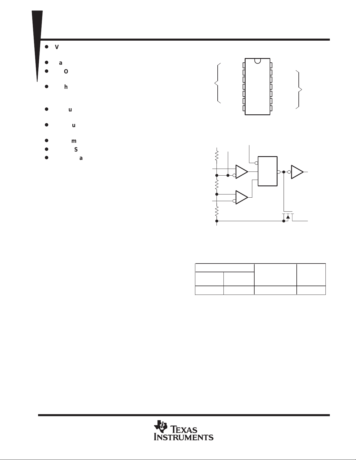
D OR N PACKAGE
(TOP VIEW)
TIMER
# 1
DSCH
THRES
CONT
RESET
OUT
TRIG
GND
1
2
3
4
5
6
7
14
13
12
11
10
9
8
V
DD
DSCH
THRES
CONT
RESET
OUT
TRIG
functional block diagram (each timer)
V
DD
CONT
R
THRES
R
TRIG
R
GND
RESET can override TRIG and THRES.
TRIG can override THRES.
RESET
R1
R1
S
TIMER
# 2
OUT
DSCH
Like the NE556, the TLC552 has a trigger level
approximately one-third of the supply voltage and
a threshold level approximately two-thirds of the
supply voltage. These levels can be altered by use
of the control voltage terminal. When the trigger
input falls below the trigger level, the flip-flop is set
and the output goes high. If the trigger input is
above the trigger level and the threshold input is
SYMBOLIZATION
DEVICE
TLC552C D,N 0°C to 70°C 3.8 mV
The D packages are available taped and reeled. Add the suffix R
to the device type when ordering (i.e., TLC552CDR).
AVAILABLE OPTIONS
PACKAGE
SUFFIX
OPERATING
TEMPERATURE
RANGE
above the threshold level, the flip-flop is reset and
the output is low. The reset input can override all other inputs and can be used to initiate a new
timing cycle. If the reset input is low, the flip-flop is reset and the output is low. Whenever the output is low, a
low-impedance path is provided between the discharge terminal and ground.
While the CMOS output is capable of sinking over 100 mA and sourcing over 10 mA, the TLC552 exhibits greatly
reduced supply-current spikes during output transitions. This minimizes the need for the large decoupling
capacitors required by the NE556.
LinCMOS is a trademark of Texas Instruments Incorporated.
PRODUCTION DATA information is current as of publication date.
Products conform to specifications per the terms of Texas Instruments
standard warranty. Production processing does not necessarily include
testing of all parameters.
Copyright 1988, Texas Instruments Incorporated
VT max
at 25°C
POST OFFICE BOX 655303 • DALLAS, TEXAS 75265
1
Page 2
TLC552C
DUAL LINCMOS TIMER
SLFS046 – FEBRUARY 1984 – REVISED MAY 1988
description (continued)
These devices have internal electrostatic discharge (ESD) protection circuits that will prevent catastrophic
failures at voltages up to 2000 V as tested under MIL-STD-883C, Method 3105.2. However, care should be
exercised in handling these devices as exposure to ESD may result in a degradation of the device parametric
performance.
All unused inputs should be tied to an appropriate logic level to prevent false triggering.
The TLC552C is characterized for operation from 0°C to 70°C.
FUNCTION TABLE
TRIGGER
RESET VOLTAGE
< MIN Irrelevant Irrelevant Low On
> MAX < MIN Irrelevant High Off
> MAX > MAX > MAX Low On
> MAX > MAX < MIN As previously established
†
For conditions shown as MIN or MAX, use the appropriate value specified under electrical characteristics.
†
VOLTAGE
†
absolute maximum ratings over operating free-air temperature range (unless otherwise noted)
Supply voltage, VDD (see Note 1) 18 V. . . . . . . . . . . . . . . . . . . . . . . . . . . . . . . . . . . . . . . . . . . . . . . . . . . . . . . . . . .
Input voltage range (any input) – 0.3 V to V
Sink current, DSCH or OUT 150 mA. . . . . . . . . . . . . . . . . . . . . . . . . . . . . . . . . . . . . . . . . . . . . . . . . . . . . . . . . . . . . .
Source current, OUT 15 mA. . . . . . . . . . . . . . . . . . . . . . . . . . . . . . . . . . . . . . . . . . . . . . . . . . . . . . . . . . . . . . . . . . . . .
Continuous total dissipation See Dissipation Rating Table. . . . . . . . . . . . . . . . . . . . . . . . . . . . . . . . . . . . . . . . . . .
Operating free-air temperature range 0°C to 75°C. . . . . . . . . . . . . . . . . . . . . . . . . . . . . . . . . . . . . . . . . . . . . . . . . .
Storage temperature range – 65°C to 150°C. . . . . . . . . . . . . . . . . . . . . . . . . . . . . . . . . . . . . . . . . . . . . . . . . . . . . . .
Lead temperature 1,6 mm (1/16 inch) from case for 10 seconds 260°C. . . . . . . . . . . . . . . . . . . . . . . . . . . . . . .
NOTES: 1. All voltage values are with respect to network ground terminal.
. . . . . . . . . . . . . . . . . . . . . . . . . . . . . . . . . . . . . . . . . . . . . . . . . . . .
THRESHOLD
VOLTAGE
†
OUTPUT
DISCHARGE
SWITCH
DD
PACKAGE
D
N
POWER RATING DERATING FACTOR ABOVE T
950 mW
1150 mW
recommended operating conditions
Supply voltage, V
Operating free-air temperature range, T
DD
A
DISSIPATION RATING TABLE
7.6 mW/°C
9.2 mW/°C
A
25°C
25°C
MIN MAX UNIT
1 18 V
0 70 °C
2
POST OFFICE BOX 655303 • DALLAS, TEXAS 75265
Page 3
Threshold voltage level
V
Threshold current
pA
Trigger voltage level
V
Trigger current
pA
Reset voltage level
V
Reset current
pA
Discharge switch on-state voltage
I
100 µA
V
Discharge switch off-state current
nA
Low-level output voltage
I
100 µA
V
High-level output voltage
I
A
V
Supply current
A
DUAL LINCMOS TIMER
SLFS046 – FEBRUARY 1984 – REVISED MAY 1988
electrical characteristics at specified free-air temperature, VDD = 1 V
PARAMETER TEST CONDITIONS T
Control voltage (open-circuit) as a percentage of supply voltage MAX 66.7%
=
OL
p
p
pp
†
Full range (MIN to MAX) is 0°C to 70°C.
OL
OH
=
= –10 µ
†
A
25°C 0.475 0.67 0.85
Full range 0.45 0.875
25°C 10
MAX 75
25°C 0.15 0.33 0.425
Full range 0.1 1.45
25°C 10
MAX 75
25°C 0.4 0.7 1
Full range 0.3 1
25°C 10
MAX 75
25°C 0.02 0.15
Full range 0.2
25°C 0.1
MAX 0.5
25°C 0.03 0.2
Full range 0.25
25°C 0.6 0.98
Full range 0.6
25°C 30 200
Full range 300
MIN TYP MAX UNIT
TLC552C
p
p
p
µ
POST OFFICE BOX 655303 • DALLAS, TEXAS 75265
3
Page 4

TLC552C
Threshold voltage level
V
Threshold current
pA
Trigger voltage level
V
Trigger current
pA
Reset voltage level
V
Reset current
pA
Discharge switch on-state voltage
I
mA
V
Discharge switch off-state current
nA
Low-level output voltage
I
mA
V
High-level output voltage
I
300 µA
V
Supply current
A
DUAL LINCMOS TIMER
SLFS046 – FEBRUARY 1984 – REVISED MAY 1988
electrical characteristics at specified free-air temperature, VDD = 2 V
PARAMETER TEST CONDITIONS T
Control voltage (open-circuit) as a percentage of supply voltage MAX 66.7%
= 1
OL
p
p
pp
†
Full range (MIN to MAX) is 0°C to 70°C.
OL
OH
= 1
= –
†
A
25°C 0.95 1.33 1.65
Full range 0.85 1.75
25°C 10
MAX 75
25°C 0.4 0.67 0.95
Full range 0.3 1.05
25°C 10
MAX 75
25°C 0.4 1.1 1.5
Full range 0.3 1.8
25°C 10
MAX 75
25°C 0.03 0.2
Full range 0.25
25°C 0.1
MAX 0.5
25°C 0.07 0.3
Full range 0.35
25°C 1.5 1.9
Full range 1.5
25°C 130 500
Full range 800
MIN TYP MAX UNIT
p
p
p
µ
4
POST OFFICE BOX 655303 • DALLAS, TEXAS 75265
Page 5

Threshold voltage level
V
Threshold current
pA
Trigger voltage level
V
Trigger current
pA
Reset voltage level
V
Reset current
pA
Discharge switch on-state voltage
I
mA
V
Discharge switch off-state current
nA
I
mA
Low-level output voltage
I
mA
V
I
mA
High-level output voltage
I
mA
V
Supply current
A
DUAL LINCMOS TIMER
SLFS046 – FEBRUARY 1984 – REVISED MAY 1988
electrical characteristics at specified free-air temperature, VDD = 5 V
PARAMETER TEST CONDITIONS T
Control voltage (open-circuit) as a percentage of supply voltage MAX 66.7%
= 10
OL
= 8
OL
p
p
pp
†
Full range (MIN to MAX) is 0°C to 70°C.
OL
OL
OH
= 5
= 3.2
= –1
†
A
25°C 2.8 3.3 3.8
Full range 2.7 3.9
25°C 10
MAX 75
25°C 1.36 1.66 1.96
Full range 1.26 2.06
25°C 10
MAX 75
25°C 0.4 1.1 1.5
Full range 0.3 1.8
25°C 10
MAX 75
25°C 0.14 0.5
Full range 0.6
25°C 0.1
MAX 0.5
25°C 0.21 0.4
Full range 0.5
25°C 0.13 0.3
Full range 0.4
25°C 0.08 0.3
Full range 0.35
25°C 4.1 4.8
Full range 4.1
25°C 340 700
Full range 1000
MIN TYP MAX UNIT
TLC552C
p
p
p
µ
POST OFFICE BOX 655303 • DALLAS, TEXAS 75265
5
Page 6

TLC552C
Threshold voltage level
V
Threshold current
pA
Trigger voltage level
V
Trigger current
pA
Reset voltage level
V
Reset current
pA
Discharge switch on-state voltage
I
100 mA
V
Discharge switch off-state current
nA
I
100 mA
Low-level output voltage
I
mA
V
I
mA
I
mA
High-level output voltage
I
mA
V
I
mA
Supply current
mA
DUAL LINCMOS TIMER
SLFS046 – FEBRUARY 1984 – REVISED MAY 1988
electrical characteristics at specified free-air temperature, VDD = 15 V
PARAMETER TEST CONDITIONS T
Control voltage (open-circuit) as a percentage of supply voltage MAX 66.7%
=
OL
=
OL
p
p
pp
†
Full range (MIN to MAX) is 0°C to 70°C.
OL
OL
OH
OH
OH
= 50
= 10
= –10
= –5
= –1
†
A
25°C 9.45 10 10.55
Full range 9.35 10.65
25°C 10
MAX 75
25°C 4.65 5 5.35
Full range 4.55 5.45
25°C 10
MAX 75
25°C 0.4 1.1 1.5
Full range 0.3 1.8
25°C 10
MAX 75
25°C 0.77 1.7
Full range 1.8
25°C 0.1
MAX 0.5
25°C 1.28 3.2
Full range 3.6
25°C 0.63 1
Full range 1.3
25°C 0.12 0.3
Full range 0.4
25°C 12.5 14.2
Full range 12.5
25°C 13.5 14.6
Full range 13.5
25°C 14.2 14.9
Full range 14.2
25°C 0.72 1.2
Full range 1.6
MIN TYP MAX UNIT
p
p
p
6
POST OFFICE BOX 655303 • DALLAS, TEXAS 75265
Page 7

Threshold voltage level
V
Threshold current
pA
Trigger voltage level
V
Trigger current
pA
Reset voltage level
V
Reset current
pA
Discharge switch on-state voltage
I
100 mA
V
Discharge switch off-state current
nA
Low-level output voltage
I
mA
V
High-level output voltage
I
mA
V
Supply current
mA
DD
,
AB
,
R
C
pF
ns
DUAL LINCMOS TIMER
SLFS046 – FEBRUARY 1984 – REVISED MAY 1988
electrical characteristics at specified free-air temperature, VDD = 18 V
PARAMETER TEST CONDITIONS T
Control voltage (open-circuit) as a percentage of supply voltage MAX 66.7%
=
OL
p
p
pp
†
Full range (MIN to MAX) is 0°C to 70°C.
OL
OH
= 3.2
= –1
†
A
25°C 11.4 12 12.6
Full range 10.9 12.7
25°C 10
MAX 75
25°C 5.6 6 6.4
Full range 5.5 6.5
25°C 10
MAX 75
25°C 0.4 1.1 1.5
Full range 0.3 1.8
25°C 10
MAX 75
25°C 0.72 1.5
Full range 1.6
25°C 0.1
MAX 0.5
25°C 0.04 0.3
Full range 0.35
25°C 17.3 17.9
Full range 17.3
25°C 0.84 1.2
Full range 1.6
MIN TYP MAX UNIT
TLC552C
p
p
p
operating characteristics, VDD = 5 V, TA = 25°C (unless otherwise noted)
PARAMETER TEST CONDITIONS MIN TYP MAX UNIT
Initial error of timing interval
Supply voltage sensitivity of timing interval
Output pulse rise time
Output pulse fall time
Maximum frequency in astable mode
‡
Timing interval error is defined as the difference between the measured value and the nominal value of a random sample.
NOTE 2: RA, RB, and CT are as defined in Figure 1.
‡
V
= 5 V to 15 V, R
CT = 0.1 µF,
= 10 MΩ,
L
RA = 470 Ω,
CT = 200 pF,
= R
See Note 2
RB = 200 Ω,
See Note 2
= 1 kΩ to 100 kΩ,
p
= 10
L
1.2 2.8 MHz
1% 3%
0.1 0.5 %/V
20 75
15 60
POST OFFICE BOX 655303 • DALLAS, TEXAS 75265
7
Page 8

TLC552C
DUAL LINCMOS TIMER
SLFS046 – FEBRUARY 1984 – REVISED MAY 1988
APPLICATION INFORMATION
V
DD
R
A
0.1 µF
R
B
C
T
0.1 µF
CONT V
RESET
DISCH
THRES
TRIG
DD
GND
OUT
R
L
Output
C
L
Figure 1. Circuit for Astable Operation
8
POST OFFICE BOX 655303 • DALLAS, TEXAS 75265
Page 9

IMPORTANT NOTICE
T exas Instruments and its subsidiaries (TI) reserve the right to make changes to their products or to discontinue
any product or service without notice, and advise customers to obtain the latest version of relevant information
to verify, before placing orders, that information being relied on is current and complete. All products are sold
subject to the terms and conditions of sale supplied at the time of order acknowledgement, including those
pertaining to warranty, patent infringement, and limitation of liability.
TI warrants performance of its semiconductor products to the specifications applicable at the time of sale in
accordance with TI’s standard warranty. Testing and other quality control techniques are utilized to the extent
TI deems necessary to support this warranty . Specific testing of all parameters of each device is not necessarily
performed, except those mandated by government requirements.
CERTAIN APPLICA TIONS USING SEMICONDUCT OR PRODUCTS MAY INVOLVE POTENTIAL RISKS OF
DEATH, PERSONAL INJURY, OR SEVERE PROPERTY OR ENVIRONMENTAL DAMAGE (“CRITICAL
APPLICATIONS”). TI SEMICONDUCTOR PRODUCTS ARE NOT DESIGNED, AUTHORIZED, OR
WARRANTED TO BE SUITABLE FOR USE IN LIFE-SUPPORT DEVICES OR SYSTEMS OR OTHER
CRITICAL APPLICA TIONS. INCLUSION OF TI PRODUCTS IN SUCH APPLICATIONS IS UNDERST OOD TO
BE FULLY AT THE CUSTOMER’S RISK.
In order to minimize risks associated with the customer’s applications, adequate design and operating
safeguards must be provided by the customer to minimize inherent or procedural hazards.
TI assumes no liability for applications assistance or customer product design. TI does not warrant or represent
that any license, either express or implied, is granted under any patent right, copyright, mask work right, or other
intellectual property right of TI covering or relating to any combination, machine, or process in which such
semiconductor products or services might be or are used. TI’s publication of information regarding any third
party’s products or services does not constitute TI’s approval, warranty or endorsement thereof.
Copyright 1998, Texas Instruments Incorporated
 Loading...