

Page 1
U
TLC542C, TLC542I
8-BIT ANALOG-TO-DIGITAL CONVERTERS
WITH SERIAL CONTROL AND 11 INPUTS
SLAS075A – FEBRUARY 1989 – REVISED MARCH 1995
D
8-Bit Resolution A/D Converter
D
Microprocessor Peripheral or Stand-Alone
Operation
D
On-Chip 12-Channel Analog Multiplexer
D
Built-in Self-Test Mode
D
Software-Controllable Sample and Hold
D
Total Unadjusted Error... ±0.5 LSB Max
D
Direct Replacement for Motorola
MC145041
D
On-Board System Clock
D
End-of-Conversion (EOC) Output
D
Pinout and Control Signals Compatible
INPUT A0
INPUT A1
INPUT A2
INPUT A3
INPUT A4
INPUT A5
INPUT A6
INPUT A7
INPUT A8
With the TLC1542/3 10-Bit A/D Converters
D
CMOS Technology
PARAMETER VALUE
Channel Acquisition/Sample Time 16 µs
Conversion TIme (Max) 20 µs
Samples per Second (Max) 25 × 10
Power Dissipation (Max) 10 mW
description
The TLC542 is a CMOS converter built around an
8-bit switched-capacitor successive-approximation
3
INPUT A3
INPUT A4
INPUT A5
INPUT A6
INPUT A7
analog-to-digital converter. The device is designed
for serial interface to a microprocessor or peripheral
via a 3-state output with three inputs [including I/O
CLOCK, CS
(chip select), and ADDRESS INPUT].
The TLC542 allows high-speed data transfers and
sample rates of up to 40,000 samples per second.
In addition to the high-speed converter and
versatile control logic, an on-chip 12-channel
analog multiplexer can sample any one of 1 1 inputs or an internal “self-test” voltage, and the sample and hold
is started under microprocessor control. At the end of conversion, the end-of-conversion (EOC) output pin goes
high to indicate that conversion is complete. Detailed information on interfacing to most popular
microprocessors is readily available from the factory.
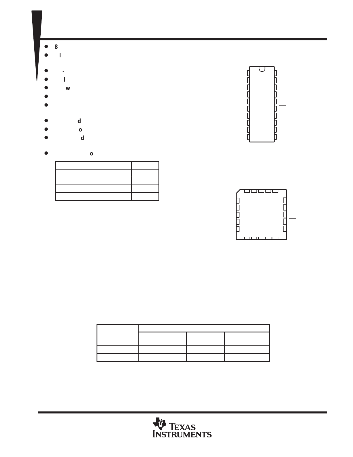
AVAILABLE OPTIONS
PACKAGE
T
A
0°C to 70°C — TLC542CN TLC542CDW
–40°C to 85°C TLC542IFN TLC542IN TLC542IDW
CHIP CARRIER
(FN)
PLASTIC DIP
(N)
DW OR N PACKAGE
(TOP VIEW)
1
2
3
4
5
6
7
8
9
GND
SMALL OUTLINE
10
FN PACKAGE
(TOP VIEW)
INPUT A2
INPUT A1
3212019
4
5
6
7
8
910111213
GND
INPUT A8
(DW)
V
20
CC
EOC
19
I/O CLOCK
18
ADDRESS INPUT
17
DATA OUT
16
CS
15
REF+
14
REF–
13
INPUT A10
12
INPUT A9
11
CC
INPUT A0
V
EOC
18
17
16
15
14
REF–
INPUT A9
INPUT A10
I/O CLOCK
ADDRESS INP
DATA OUT
CS
REF+
PRODUCTION DATA information is current as of publication date.
Products conform to specifications per the terms of Texas Instruments
standard warranty. Production processing does not necessarily include
testing of all parameters.
POST OFFICE BOX 655303 • DALLAS, TEXAS 75265
Copyright 1995, Texas Instruments Incorporated
1
Page 2
TLC542C, TLC542I
8-BIT ANALOG-TO-DIGITAL CONVERTERS
WITH SERIAL CONTROL AND 11 INPUTS
SLAS075A – FEBRUARY 1989 – REVISED MARCH 1995
description (continued)
The converter incorporated in the TLC542 features differential high-impedance reference inputs that facilitate
ratiometric conversion, scaling, and isolation of analog circuitry from logic and supply noises. A switchedcapacitor design allows low-error (±0.5 LSB) conversion in 20 µs over the full operating temperature range.
The TLC542C is characterized for operation from 0°C to 70°C and the TLC542I is characterized for operation
from –40°C to 85°C.
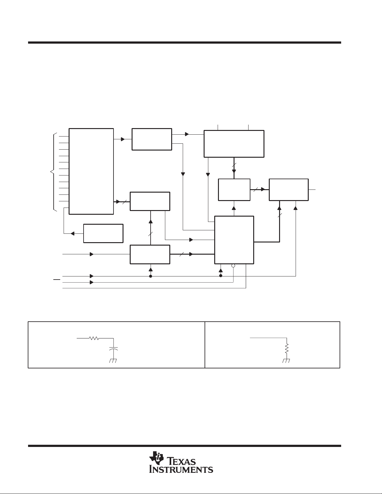
functional block diagram
REF+ REF–
Analog
Inputs
ADDRESS
INPUT
I/O CLOCK
CS
EOC
12-Channel
Analog
Multiplexer
Self-Test
Reference
typical equivalent inputs
Sample and
4
Input Address
Register
Multiplexer
Hold
4
Input
8-Bit
Analog-to-Digital
Converter
(Switched-Capacitors)
8
Output
Data
Register
Control Logic
and I/O
2
Counters
8
8-to-1 Data
Selector and
Driver
4
DATA
OUT
INPUT CIRCUIT IMPEDANCE DURING SAMPLING MODE INPUT CIRCUIT IMPEDANCE DURING HOLD MODE
INPUT
A0–A10
2
1 kΩ TYP
Ci = 60 pF TYP
(equivalent input
capacitance)
POST OFFICE BOX 655303 • DALLAS, TEXAS 75265
INPUT
A0–A10
5 MΩ TYP
Page 3
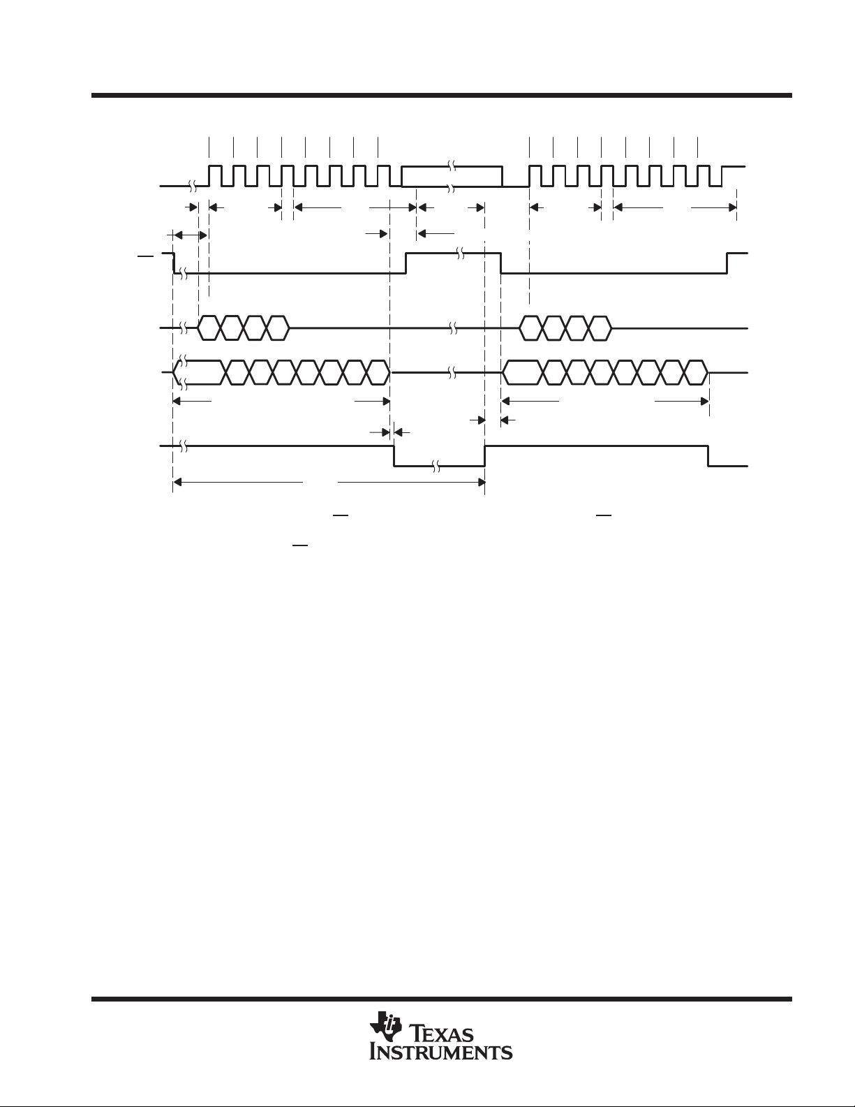
operating sequence
1 2345678 1 2345678
I/O
CLOCK
t
t
su(CS)
CS
su(A)
(see Note A)
Access
Cycle B
t
acq
8-BIT ANALOG-TO-DIGITAL CONVERTERS
WITH SERIAL CONTROL AND 11 INPUTS
Don’t Care
t
conv
12 Internal System Clocks ≤ 12 µs
TLC542C, TLC542I
SLAS075A – FEBRUARY 1989 – REVISED MARCH 1995
Access
Cycle C
t
acq
MSB LSB
ADDRESS
INPUT
DATA
OUT
EOC
NOTES: A. To minimize errors caused by noise at the chip select input, the internal circuitry waits for two rising edges and one falling edge
B. The output is 3-stated on CS
B3 B2 B1 B0 C3 C2 C1 C0
Previous Conversion Data A Conversion Data B
MSB
(see Note B)
of the internal system clock after CS
specifications. Therefore, no attempt should be made to clock-in an address until the minimum chip select setup time has elapsed.
Don’t Care Don’t Care
Hi-Z State
See Note B
LSB
t
t
d(I/O–EOC)
t
cycle
↓ before responding to control input signals. The CS setup time is given by the t
going high or on the negative edge of the eighth I/O clock.
d(EOC–DATA)
MSB LSB
B7 B6 B5 B4 B3 B2 B1 B0A7 A6 A5 A4 A3 A2 A1 A0
MSB LSB
Hi-Z
State
su(CS)
absolute maximum ratings over operating free-air temperature range (unless otherwise noted)
Supply voltage, V
Input voltage range (any input) –0.3 V to V
Output voltage range –0.3 V to V
Peak input current range (any input) ±20 mA. . . . . . . . . . . . . . . . . . . . . . . . . . . . . . . . . . . . . . . . . . . . . . . . . . . . . .
Peak total input current (all inputs) ±30 mA. . . . . . . . . . . . . . . . . . . . . . . . . . . . . . . . . . . . . . . . . . . . . . . . . . . . . . . .
Operating free-air temperature range: TLC542C 0°C to 70°C. . . . . . . . . . . . . . . . . . . . . . . . . . . . . . . . . . . . . . . .
Storage temperature range –65°C to 150°C. . . . . . . . . . . . . . . . . . . . . . . . . . . . . . . . . . . . . . . . . . . . . . . . . . . . . . .
Case temperature for 10 seconds: FN package 260°C. . . . . . . . . . . . . . . . . . . . . . . . . . . . . . . . . . . . . . . . . . . . .
Lead temperature 1,6 mm (1/16 inch) from case for 10 seconds: DW or N package 260°C. . . . . . . . . . . . . .
†
Stresses beyond those listed under “absolute maximum ratings” may cause permanent damage to the device. These are stress ratings only, and
functional operation of the device at these or any other conditions beyond those indicated under “recommended operating conditions” is not
implied. Exposure to absolute-maximum-rated conditions for extended periods may affect device reliability.
NOTE 1: All voltage values are with respect to digital ground with REF– and GND wired together (unless otherwise noted).
(see Note 1) 6.5 V. . . . . . . . . . . . . . . . . . . . . . . . . . . . . . . . . . . . . . . . . . . . . . . . . . . . . . . . . .
CC
TLC542l –40°C to 85°C. . . . . . . . . . . . . . . . . . . . . . . . . . . . . . . . . . . . . .
CC
CC
+ 0.3 V. . . . . . . . . . . . . . . . . . . . . . . . . . . . . . . . . . . . . . . . . . . . . .
+ 0.3 V. . . . . . . . . . . . . . . . . . . . . . . . . . . . . . . . . . . . . . . . . . . . . . . . . . . . . . .
†
POST OFFICE BOX 655303 • DALLAS, TEXAS 75265
3
Page 4
TLC542C, TLC542I
I/O CLOCK transition time, t
(see Note 3)
ns
Operating free-air temperature, T
°C
(g )
A
Selected channel leakage current
CC
,
A
CiInput capacitance
pF
8-BIT ANALOG-TO-DIGITAL CONVERTERS
WITH SERIAL CONTROL AND 11 INPUTS
SLAS075A – FEBRUARY 1989 – REVISED MARCH 1995
recommended operating conditions, V
Supply voltage, V
Positive reference voltage, V
Negative reference voltage, V
Differential reference voltage, V
Analog input voltage (see Note 3) 0 V
High-level control input voltage, V
Low-level control input voltage, V
Setup time, address bits at data input before I/O CLOCK↑, t
Hold time, address bits after I/O CLOCK↑, t
Hold time, CS low after 8th I/O CLOCK↑, t
Setup time, CS low before clocking in first address bit, t
Input/output clock frequency, f
Input/output clock high, t
Input/output clock low, t
p
NOTES: 2. Analog input voltages greater than that applied to REF+ convert as all ones (11111111), while input voltages less than that applied
CC
(see Note 2) V
ref+
(see Note 2) –0.1 0 V
ref–
– V
ref+
IH
IL
clock(I/O)
wH(I/O)
wL(I/O)
t
p
to REF – convert as all zeros (00000000). For proper operation, REF+ must be at least 1 V higher than REF–. Also, the total
unadjusted error may increase as this differential reference voltage falls below 4.75 V.
3. This is the time required for the clock input signal to fall from VIH min to VIL max or to rise from VIL max to VIH min. In the vicinity
of normal room temperature, the devices function with input clock transition time as slow as 2 µs for remote data acquisition
applications where the sensor and the A/D converter are placed several feet away from the controlling microprocessor.
4. To minimize errors caused by noise at the chip select input, the internal circuitry waits for two rising edges and one falling edge of
the internal system clock after CS
specifications. Therefore, no attempt should be made to clock-in address data until the minimum chip select setup time has elapsed.
A
(see Note 2) 1 V
ref–
h(A)
h(CS)
f
clock(I/O)
f
clock(I/O)
TLC542C 0 70
TLC542I –40 85
↓ before responding to control input signals. The CS setup time is given by the t
= 4.75 to 5.5 V
CC
MIN NOM MAX UNIT
4.75 5 5.5 V
ref–VCC
2 V
su(A)
(see Note 4) 3.8 µs
su(CS)
≤ 525 kHz 100
> 525 kHz 40
400 ns
0 ns
0 ns
0 1.1 MHz
404 ns
404 ns
VCC + 0.1 V
CCVCC
ref+
+ 0.2 V
CC
V
V
0.8 V
°
su(CS)
electrical characteristics over recommended operating temperature range, VCC = V
= 1.1 MHz (unless otherwise noted)
5.5 V, f
V
V
I
I
I
I
†
clock(I/O)
High-level output voltage (DATA OUT) VCC = 4.75 V, IOH = –360 µA 2.4 V
OH
Low-level output voltage VCC = 4.75 V, IOL = 1.6 mA 0.4 V
OL
Off-state (high-impedance state)
output current
High-level input current VI = V
IH
Low-level input current VI = 0 –0.005 –2.5 µA
IL
Operating supply current CS at 0 V 1.2 2 mA
CC
Maximum static analog reference current into
ref
REF+
p
All typical values are at TA = 25°C.
PARAMETER TEST CONDITIONS MIN TYP†MAX UNIT
VO = VCC, CS at V
VO = 0,
CC
Selected at V
Unselected channel at 0 V
V
= VCC, V
ref+
p
Analog inputs 7 55
Control inputs 5 15
,
CC
CS at V
CC
0.005 2 µA
0°C to 70 °C 0.4
–40°C to 85°C –0.4
= GND 10 µA
ref–
= 4.75 V to
ref+
–10
10
µ
µ
p
4
POST OFFICE BOX 655303 • DALLAS, TEXAS 75265
Page 5

TLC542C, TLC542I
8-BIT ANALOG-TO-DIGITAL CONVERTERS
WITH SERIAL CONTROL AND 11 INPUTS
SLAS075A – FEBRUARY 1989 – REVISED MARCH 1995
operating characteristics over recommended operating free-air temperature range,
= V
V
CC
E
L
E
ZS
E
FS
t
conv
t
cycle
t
acq
t
v
t
d(IO-DATA)
t
d(IO-EOC)
t
d(EOC-DATA)
t
, t
PZH
PZL
t
, t
PHZ
PLZ
t
r(EOC)
t
f(EOC)
t
r(bus)
t
f(bus)
†
All typical values are at TA = 25°C
NOTES: 2. Analog input voltages greater than that applied to REF+ convert to all ones (11111111), while input voltages less than that applied
= 4.75 to 5.5 V, f
ref+
PARAMETER TEST CONDITIONS MIN TYP
Linearity error (see Note 5) ±0.5 LSB
Zero-scale error (see Note 6) See Note 2 ±0.5 LSB
Full-scale error (see Note 6) See Note 2 ±0.5 LSB
Total unadjusted error (see Note 7) ±0.5 LSB
Self-test output code
Conversion time See operating sequence 20 µs
Total access and conversion cycle time See operating sequence 40 µs
Channel acquisition time (sample cycle) See operating sequence 16 µs
Time ouput data remains valid after I/O CLK↓ See Figure 5 10 ns
Delay time, I/O CLK↓ to data output valid See Figure 5 400 ns
Delay time, 8th I/O CLK↓ to EOC↓ See Figure 6 500 ns
Delay time, EOC↑ to data out (MSB) See Figure 7 400 ns
Delay time, CS↓ to data out (MSB) See Figure 2 3.4 µs
Delay time, CS↑ to data out (MSB) See Figure 2 150 ns
Rise time See Figure 7 100 ns
Fall time See Figure 6 100 ns
Data bus rise time See Figure 5 300 ns
Data bus fall time See Figure 5 300 ns
to REF – convert to all zeros (00000000). For proper operation, REF+ must be at least 1 V higher than REF–. Also, the total
unadjusted error may increase as this differential reference voltage falls below 4.75 V.
5. Linearity error is the maximum deviation from the best straight line through the A/D transfer characteristics.
6. Zero-scale Error is the difference between 00000000 and the converted output for zero input voltage; full-scale error is the dif ference
between 11111111 and the converted output for full-scale input voltage.
7. Total unadjusted error is the sum of linearity, zero-scale, and full-scale errors.
8. Both the input address and the output codes are expressed in positive logic. The A1 1 analog input signal is internally genera ted and
is used for test purposes.
clock(I/O)
= 1 MHZ
Input A11 address = 1011,
See Note 8
01111101
(126)
128
†
1000001 1
MAX UNIT
(130)
POST OFFICE BOX 655303 • DALLAS, TEXAS 75265
5
Page 6

TLC542C, TLC542I
8-BIT ANALOG-TO-DIGITAL CONVERTERS
WITH SERIAL CONTROL AND 11 INPUTS
SLAS075A – FEBRUARY 1989 – REVISED MARCH 1995
PARAMETER MEASUREMENT INFORMATION
CS
t
PZH
DATA OUT
1.4 V
Output
Under Test
C
(see Note A)
LOAD CIRCUIT FOR
NOTE A: CL = 50 pF
, t
PZL
L
td, tr, AND t
0.8 V
2.4 V
0.4 V
3 kΩ
f
Test
Point
2 V
Output
Under Test
C
(see Note A)
L
LOAD CIRCUIT FOR
t
AND t
PZH
PHZ
Figure 1. Load Circuits
t
, t
PHZ
PLZ
90%
10%
CLOCK
A
I/O
3 kΩ
n
Test
Point
Output
Under Test
(see Note A)
LOAD CIRCUIT FOR
t
PZL
Address
Valid
2 V
0.8 V
t
su(A)
2 V
C
L
V
CC
AND t
3 kΩ
PLZ
Test
Point
t
h(A)
Figure 2. CS to Data Output Timing
CS
I/O CLOCK
t
su(CS)
0.8 V
2 V
Figure 4. Figure 4. CS to I/O CLOCK Timing
Figure 3. Address Timing
2 V
8th
Clock
0.8 V
t
h(CS)
6
POST OFFICE BOX 655303 • DALLAS, TEXAS 75265
Page 7

TLC542C, TLC542I
8-BIT ANALOG-TO-DIGITAL CONVERTERS
WITH SERIAL CONTROL AND 11 INPUTS
SLAS075A – FEBRUARY 1989 – REVISED MARCH 1995
PARAMETER MEASUREMENT INFORMATION
t
t
f(I/O)
r(I/O)
I/O CLOCK
t
DATA OUT
I/O CLOCK
EOC
2 V
0.8 V
f
d(I/O-DATA)
t
v
2.4 V
0.4 V
2.4 V
0.4 V
Figure 5. Data Output Timing
8th
Clock
t
d(I/O-EOC)
t
f(EOC)
Figure 6. EOC Timing
2 V
0.8 V
clock(I/O)
t
r(bus)
0.8 V
2.4 V
, t
0.8 V
f(bus)
0.4 V
EOC
DATA OUT
t
r(EOC)
0.4 V
2.4 V
t
d(EOC-DATA)
2.4 V
0.4 V
Figure 7. Data Output to EOC Timing
Valid MSB
POST OFFICE BOX 655303 • DALLAS, TEXAS 75265
7
Page 8

TLC542C, TLC542I
8-BIT ANALOG-TO-DIGITAL CONVERTERS
WITH SERIAL CONTROL AND 11 INPUTS
SLAS075A – FEBRUARY 1989 – REVISED MARCH 1995
APPLICATION INFORMATION
simplified analog input analysis
Using the equivalent circuit in Figure 8, the time required to charge the analog input capacitance from 0 to V
within 1/2 LSB can be derived as follows:
The capacitance charging voltage is given by
–t
= VS 1–e
V
C
( )
c/RtCi
where
= Rs + r
R
t
i
The final voltage to 1/2 LSB is given by
(1/2 LSB) = VS – (VS/512)
C
Equating equation 1 to equation 2 and solving for time t
–t
–(VS/512) = VS 1–e
V
S
( )
c/RtCi
gives
c
and
t
(1/2 LSB) = Rt × Ci × ln(512) (4)
c
Therefore, with the values given the time for the analog input signal to settle is
(1/2 LSB) = (Rs + 1 kΩ) × 60 pF × ln(512)
t
c
(5)
This time must be less than the converter sample time shown in the timing diagrams.
Driving Source
†
TLC542
S
(1)
(2)V
(3)
R
s
V
S
VI= Input Voltage at INPUT A0–A10
VS= External Driving Source Voltage
Rs= Source Resistance
ri= Input Resistance
Ci= Input Capacitance
†
Driving source requirements:
• Noise and distortion for the source must be equivalent to the
resolution of the converter.
• Rs must be real at the input frequency.
V
I
r
i
1 kΩ MAX
V
C
C
i
50 pF MAX
Figure 8. Equivalent Input Circuit Including the Driving Source
8
POST OFFICE BOX 655303 • DALLAS, TEXAS 75265
Page 9

TLC542C, TLC542I
8-BIT ANALOG-TO-DIGITAL CONVERTERS
WITH SERIAL CONTROL AND 11 INPUTS
SLAS075A – FEBRUARY 1989 – REVISED MARCH 1995
PRINCIPLES OF OPERATION
The TLC542 is a complete data acquisition system on a single chip. The device includes such functions as analog
multiplexer, sample and hold, 8-bit A/D converter, data and control registers, and control logic. Three control inputs
(I/O CLOCK, CS
inputs and a TTL-compatible 3-state output are intended for serial communications with a microprocessor or
microcomputer. With judicious interface timing, the TLC542 can complete a conversion in 20 µs, while complete
input-conversion-output cycles can be repeated every 40 µs. Furthermore, this fast conversion can be executed on
any of 11 inputs or its built-in self-test and in any order desired by the controlling processor.
(chip select), and ADDRESS INPUT) are included for flexibility and access speed. These control
When CS
terminals are disabled. When additional TLC542 devices are used, this feature allows each of these terminals, with
the exception of the CS
devices. Thus, this feature minimizes the control logic terminals required when using multiple A/D devices.
The control sequence is designed to minimize the time and effort required to initiate conversion and obtain the
conversion result. A normal control sequence is as follows:
CS
can be kept low during periods of multiple conversion. If CS is taken high, it must remain high until the end of
conversion. Otherwise, a valid falling edge of CS
is high, the DATA OUT terminal is in a 3-state condition, and the ADDRESS INPUT and I/O CLOCK
terminal, to share a control logic point with their counterpart terminals on additional A/D
1. CS
2. On the first four rising edges of the I/O CLOCK, a new positive-logic multiplexer address is shifted in, with
3. Three clock cycles are applied to the I/O CLOCK terminal and the sixth, seventh, and eighth conversion
4. The final eighth clock cycle is applied to the I/O CLOCK terminal. The falling edge of this clock cycle initiates
is brought low. To minimize errors caused by noise at the CS input, the internal circuitry waits for two
rising edges and then a falling edge of the internal system clock before recognizing the low CS
The MSB of the result of the previous conversion automatically appears on the DATA OUT terminal.
the MSB of this address shifted first. The negative edges of these four I/O CLOCK pulses shift out the
second, third, fourth, and fifth most significant bits of the result of the previous conversion. The on-chip
sample and hold begins sampling the newly addressed analog input after the fourth falling edge of the I/O
CLOCK. The sampling operation basically involves charging the internal capacitors to the level of the analog
input voltage.
bits are shifted out on the negative edges of these clock cycles.
a 12-system clock (≈ 12 µs) additional sampling period while the output is in the high-impedance state.
Conversion is then performed during the next 20 µs. After this final I/O CLOCK cycle, CS
the I/O CLOCK must remain low for at least 20 µs to allow for the conversion function.
causes a reset condition, which aborts the conversion process.
transition.
must go high or
A new conversion may be started and the ongoing conversion simultaneously aborted by performing steps 1 through
4 before the 20-µs conversion time has elapsed. Such action yields the conversion result of the previous conversion
and not the ongoing conversion.
The end-of-conversion (EOC) output goes low on the negative edge of the eighth I/O CLOCK. The subsequent
low-to-high transition of EOC indicates the A/D conversion is complete and the conversion is ready for transfer.
POST OFFICE BOX 655303 • DALLAS, TEXAS 75265
9
Page 10

TLC542C, TLC542I
8-BIT ANALOG-TO-DIGITAL CONVERTERS
WITH SERIAL CONTROL AND 11 INPUTS
SLAS075A – FEBRUARY 1989 – REVISED MARCH 1995
10
POST OFFICE BOX 655303 • DALLAS, TEXAS 75265
Page 11

IMPORTANT NOTICE
T exas Instruments and its subsidiaries (TI) reserve the right to make changes to their products or to discontinue
any product or service without notice, and advise customers to obtain the latest version of relevant information
to verify, before placing orders, that information being relied on is current and complete. All products are sold
subject to the terms and conditions of sale supplied at the time of order acknowledgement, including those
pertaining to warranty, patent infringement, and limitation of liability.
TI warrants performance of its semiconductor products to the specifications applicable at the time of sale in
accordance with TI’s standard warranty. Testing and other quality control techniques are utilized to the extent
TI deems necessary to support this warranty . Specific testing of all parameters of each device is not necessarily
performed, except those mandated by government requirements.
CERT AIN APPLICATIONS USING SEMICONDUCTOR PRODUCTS MAY INVOLVE POTENTIAL RISKS OF
DEATH, PERSONAL INJURY, OR SEVERE PROPERTY OR ENVIRONMENTAL DAMAGE (“CRITICAL
APPLICATIONS”). TI SEMICONDUCTOR PRODUCTS ARE NOT DESIGNED, AUTHORIZED, OR
WARRANTED TO BE SUITABLE FOR USE IN LIFE-SUPPORT DEVICES OR SYSTEMS OR OTHER
CRITICAL APPLICA TIONS. INCLUSION OF TI PRODUCTS IN SUCH APPLICATIONS IS UNDERST OOD TO
BE FULLY AT THE CUSTOMER’S RISK.
In order to minimize risks associated with the customer’s applications, adequate design and operating
safeguards must be provided by the customer to minimize inherent or procedural hazards.
TI assumes no liability for applications assistance or customer product design. TI does not warrant or represent
that any license, either express or implied, is granted under any patent right, copyright, mask work right, or other
intellectual property right of TI covering or relating to any combination, machine, or process in which such
semiconductor products or services might be or are used. TI’s publication of information regarding any third
party’s products or services does not constitute TI’s approval, warranty or endorsement thereof.
Copyright 1999, Texas Instruments Incorporated
 Loading...