

Page 1
TLC320AD535C/I
Dual Channel V oice/Data Codec
2000 Mixed Signal Products
Data Manual
SLAS202B
Page 2

IMPORTANT NOTICE
T exas Instruments and its subsidiaries (TI) reserve the right to make changes to their products or to discontinue
any product or service without notice, and advise customers to obtain the latest version of relevant information
to verify, before placing orders, that information being relied on is current and complete. All products are sold
subject to the terms and conditions of sale supplied at the time of order acknowledgement, including those
pertaining to warranty, patent infringement, and limitation of liability.
TI warrants performance of its semiconductor products to the specifications applicable at the time of sale in
accordance with TI’s standard warranty. Testing and other quality control techniques are utilized to the extent
TI deems necessary to support this warranty. Specific testing of all parameters of each device is not necessarily
performed, except those mandated by government requirements.
CERT AIN APPLICATIONS USING SEMICONDUCTOR PRODUCTS MAY INVOLVE POTENTIAL RISKS OF
DEATH, PERSONAL INJURY, OR SEVERE PROPERTY OR ENVIRONMENTAL DAMAGE (“CRITICAL
APPLICATIONS”). TI SEMICONDUCTOR PRODUCTS ARE NOT DESIGNED, AUTHORIZED, OR
WARRANTED TO BE SUITABLE FOR USE IN LIFE-SUPPORT DEVICES OR SYSTEMS OR OTHER
CRITICAL APPLICATIONS. INCLUSION OF TI PRODUCTS IN SUCH APPLICA TIONS IS UNDERSTOOD T O
BE FULLY AT THE CUSTOMER’S RISK.
In order to minimize risks associated with the customer’s applications, adequate design and operating
safeguards must be provided by the customer to minimize inherent or procedural hazards.
TI assumes no liability for applications assistance or customer product design. TI does not warrant or represent
that any license, either express or implied, is granted under any patent right, copyright, mask work right, or other
intellectual property right of TI covering or relating to any combination, machine, or process in which such
semiconductor products or services might be or are used. TI’s publication of information regarding any third
party’s products or services does not constitute TI’s approval, warranty or endorsement thereof.
Copyright 2000, Texas Instruments Incorporated
Page 3

iii
Contents
Section Title Page
1 Introduction 1–1. . . . . . . . . . . . . . . . . . . . . . . . . . . . . . . . . . . . . . . . . . . . . . . . . . . . . .
1.1 Features 1–1. . . . . . . . . . . . . . . . . . . . . . . . . . . . . . . . . . . . . . . . . . . . . . . . . . .
1.2 Functional Block Diagram 1–2. . . . . . . . . . . . . . . . . . . . . . . . . . . . . . . . . . . .
1.3 Voice Channel Codec Logic Diagram 1–3. . . . . . . . . . . . . . . . . . . . . . . . . .
1.4 Data Channel Codec Logic Diagram 1–4. . . . . . . . . . . . . . . . . . . . . . . . . . .
1.5 Terminal Assignments 1–4. . . . . . . . . . . . . . . . . . . . . . . . . . . . . . . . . . . . . . . .
1.6 Ordering Information 1–5. . . . . . . . . . . . . . . . . . . . . . . . . . . . . . . . . . . . . . . . .
1.7 Terminal Functions 1–5. . . . . . . . . . . . . . . . . . . . . . . . . . . . . . . . . . . . . . . . . .
2 Functional Description 2–1. . . . . . . . . . . . . . . . . . . . . . . . . . . . . . . . . . . . . . . . . . . .
2.1 Device Requirements and System Overview 2–1. . . . . . . . . . . . . . . . . . . .
2.2 Codec Functions 2–1. . . . . . . . . . . . . . . . . . . . . . . . . . . . . . . . . . . . . . . . . . . .
2.3 Hybrid Functions 2–1. . . . . . . . . . . . . . . . . . . . . . . . . . . . . . . . . . . . . . . . . . . .
2.4 Voice Channel Analog 2–1. . . . . . . . . . . . . . . . . . . . . . . . . . . . . . . . . . . . . . . .
2.5 Miscellaneous Logic and Other Circuitry 2–1. . . . . . . . . . . . . . . . . . . . . . . .
3 Codec Functional Description 3–1. . . . . . . . . . . . . . . . . . . . . . . . . . . . . . . . . . . . .
3.1 Operating Frequencies 3–1. . . . . . . . . . . . . . . . . . . . . . . . . . . . . . . . . . . . . . .
3.2 ADC Signal Channel 3–1. . . . . . . . . . . . . . . . . . . . . . . . . . . . . . . . . . . . . . . . .
3.3 DAC Signal Channel 3–1. . . . . . . . . . . . . . . . . . . . . . . . . . . . . . . . . . . . . . . . .
3.4 Sigma-Delta ADC 3–1. . . . . . . . . . . . . . . . . . . . . . . . . . . . . . . . . . . . . . . . . . .
3.5 Decimation Filter 3–1. . . . . . . . . . . . . . . . . . . . . . . . . . . . . . . . . . . . . . . . . . . .
3.6 Sigma-Delta DAC 3–2. . . . . . . . . . . . . . . . . . . . . . . . . . . . . . . . . . . . . . . . . . .
3.7 Interpolation Filter 3–2. . . . . . . . . . . . . . . . . . . . . . . . . . . . . . . . . . . . . . . . . . .
3.8 Analog and Digital Loopbacks 3–2. . . . . . . . . . . . . . . . . . . . . . . . . . . . . . . . .
3.9 Software Power Down 3–2. . . . . . . . . . . . . . . . . . . . . . . . . . . . . . . . . . . . . . .
3.10 Reset Circuit 3–2. . . . . . . . . . . . . . . . . . . . . . . . . . . . . . . . . . . . . . . . . . . . . . . .
3.11 Test Module 3–3. . . . . . . . . . . . . . . . . . . . . . . . . . . . . . . . . . . . . . . . . . . . . . . .
4 Serial Communications 4–1. . . . . . . . . . . . . . . . . . . . . . . . . . . . . . . . . . . . . . . . . . .
4.1 Primary Serial Communication 4–1. . . . . . . . . . . . . . . . . . . . . . . . . . . . . . . .
4.1.1 FS High Mode Primary Communication Timing 4–2. . . . . . . . .
4.1.2 FS Low Mode Primary Communication Timing 4–2. . . . . . . . . .
4.2 Secondary Serial Communication 4–3. . . . . . . . . . . . . . . . . . . . . . . . . . . . .
4.2.1 FS High Mode Secondary Communication Timing 4–4. . . . . . .
4.2.2 FS Low Mode Secondary Communication Timing 4–4. . . . . . .
5 Specifications 5–1. . . . . . . . . . . . . . . . . . . . . . . . . . . . . . . . . . . . . . . . . . . . . . . . . . . .
5.1 Absolute Maximum Ratings Over Operating Free-Air
Temperature Range 5–1. . . . . . . . . . . . . . . . . . . . . . . . . . . . . . . . . . . . . . . . . .
5.2 Recommended Operating Conditions 5–1. . . . . . . . . . . . . . . . . . . . . . . . . .
Page 4

iv
5.3 Electrical Characteristics Over Operating Free-Air Temperature
Range, DV
DD
= 5 V/3.3 V, xAVDD = 5 V/3.3 V,
MV
DD
= 5 V/3.3 V 5–1. . . . . . . . . . . . . . . . . . . . . . . . . . . . . . . . . . . . . . . . . . .
5.3.1 Digital Inputs and Outputs, f
s
= 8 kHz,
Outputs Not Loaded 5–1. . . . . . . . . . . . . . . . . . . . . . . . . . . . . . . . .
5.3.2 ADC Channel, f
s
= 8 kHz 5–2. . . . . . . . . . . . . . . . . . . . . . . . . . . .
5.3.3 ADC Dynamic Performance, f
s
= 8 kHz 5–2. . . . . . . . . . . . . . . .
5.3.3.1 ADC Signal-to-Noise 5–2. . . . . . . . . . . . . . . . . . . . .
5.3.3.2 ADC Signal-to-Distortion 5–2. . . . . . . . . . . . . . . . . .
5.3.3.3 ADC Signal-to-Distortion + Noise 5–2. . . . . . . . . .
5.3.4 ADC Characteristics 5–3. . . . . . . . . . . . . . . . . . . . . . . . . . . . . . . .
5.3.5 DAC Channel, f
s
= 8 kHz 5–3. . . . . . . . . . . . . . . . . . . . . . . . . . . .
5.3.6 DAC Dynamic Performance 5–3. . . . . . . . . . . . . . . . . . . . . . . . . .
5.3.6.1 DAC Signal-to-Noise 5–3. . . . . . . . . . . . . . . . . . . . .
5.3.6.2 DAC Signal-to-Distortion 5–3. . . . . . . . . . . . . . . . . .
5.3.6.3 DAC Signal-to-Distortion + Noise 5–3. . . . . . . . . .
5.3.7 DAC Characteristics 5–4. . . . . . . . . . . . . . . . . . . . . . . . . . . . . . . .
5.3.8 Logic DC Electrical Characteristics 5–4. . . . . . . . . . . . . . . . . . . .
5.3.9 Power Supply Rejection 5–4. . . . . . . . . . . . . . . . . . . . . . . . . . . . .
5.3.10 Power Supply 5–4. . . . . . . . . . . . . . . . . . . . . . . . . . . . . . . . . . . . . .
5.3.11 Reset Circuit 5–5. . . . . . . . . . . . . . . . . . . . . . . . . . . . . . . . . . . . . . .
5.3.12 Flash Write Enable Circuit 5–5. . . . . . . . . . . . . . . . . . . . . . . . . . .
5.3.13 8-Ω Drive 5–5. . . . . . . . . . . . . . . . . . . . . . . . . . . . . . . . . . . . . . . . . .
5.4 Timing Characteristics 5–5. . . . . . . . . . . . . . . . . . . . . . . . . . . . . . . . . . . . . . .
5.4.1 Timing Requirements 5–5. . . . . . . . . . . . . . . . . . . . . . . . . . . . . . . .
5.4.2 Switching Characteristics 5–5. . . . . . . . . . . . . . . . . . . . . . . . . . . .
5.5 Parameter Measurement Information 5–6. . . . . . . . . . . . . . . . . . . . . . . . . .
6 Application Information 6–1. . . . . . . . . . . . . . . . . . . . . . . . . . . . . . . . . . . . . . . . . . .
A Programmable Register Set A–1. . . . . . . . . . . . . . . . . . . . . . . . . . . . . . . . . . . . . . .
B Mechanical Data B–1. . . . . . . . . . . . . . . . . . . . . . . . . . . . . . . . . . . . . . . . . . . . . . . . . .
Page 5

v
List of Illustrations
Figure Title Page
4–1 Primary Communication DIN and DOUT Data Format 4–1. . . . . . . . . . . . . . . . .
4–2 FS High Mode Primary Serial Communication Timing 4–2. . . . . . . . . . . . . . . . . .
4–3 FS Low Mode Primary Serial Communication Timing 4–2. . . . . . . . . . . . . . . . . .
4–4 Secondary Communication DIN and DOUT Data Format 4–3. . . . . . . . . . . . . . .
4–5 FS Output During Software Secondary Serial Communication Request
(FS High Mode) 4–4. . . . . . . . . . . . . . . . . . . . . . . . . . . . . . . . . . . . . . . . . . . . . . . .
4–6 FS Output During Software Secondary Serial Communication Request
(FS Low Mode) 4–4. . . . . . . . . . . . . . . . . . . . . . . . . . . . . . . . . . . . . . . . . . . . . . . . .
5–1 Serial Communication Timing for FS High Mode 5–6. . . . . . . . . . . . . . . . . . . . . .
5–2 ADC Decimation Filter Response 5–6. . . . . . . . . . . . . . . . . . . . . . . . . . . . . . . . . . .
5–3 ADC Decimation Filter Passband Ripple 5–7. . . . . . . . . . . . . . . . . . . . . . . . . . . . .
5–4 DAC Interpolation Filter Response 5–7. . . . . . . . . . . . . . . . . . . . . . . . . . . . . . . . . .
5–5 DAC Interpolation Filter Passband Ripple 5–8. . . . . . . . . . . . . . . . . . . . . . . . . . . .
6–1 Functional Block of a Typical Application 6–1. . . . . . . . . . . . . . . . . . . . . . . . . . . . .
6–2 Voice Channel Codec Typical Application 6–2. . . . . . . . . . . . . . . . . . . . . . . . . . . .
6–3 Data Channel Codec Typical Application 6–3. . . . . . . . . . . . . . . . . . . . . . . . . . . . .
List of Tables
Table Title Page
4–1 Least-Significant-Bit Control Function 4–3. . . . . . . . . . . . . . . . . . . . . . . . . . . . . . . .
Page 6

vi
Page 7

1–1
1 Introduction
The TLC320AD535 dual channel voice/data codec is a mixed-signal broadband connectivity device. The
TLC320AD535 is comprised of a two-channel codec and analog hybrid circuitry with two independent serial ports for
communication with the host processor and external resistors and capacitors for setting gain and filter poles. The
device also contains microphone bias and amplification, audio mixing capabilities in the voice channel,
programmable gain control, and three (SPKR_LEFT, SPKR_RIGHT, and MONOUT) speaker drivers.The device
operates with either a 5-V analog, a 5-V digital, and a 5-V monitor power supply or a 3.3-V analog, a 3.3-V digital,
and a 5-V monitor power supply or 5-V analog, 3.3-V digital, and 5-V monitor power supply . It is available in a single
64-pin PM (QFP) package.
1.1 Features
• Analog, Digital, and Monitor Amp Power Supplies: 5 V or 3.3 V
• Separate Software Power-Down Modes for Data and Voice Channels
• Independent Voice and Data Channel Sample Rates up to 11.025 kHz
• 16-Bit Signal Processing
• Dynamic Range of 80 dB in the Data and Voice Channels
• Total Signal-to-Noise + Distortion of 77 dB for the ADCs
• Total Signal-to-Noise + Distortion of 74 dB for the DACs
• Programmable Gain Amplifiers
• 600-Ω T API Audio and Data Channel Drivers
• 60-Ω Headphone Driver With Programmable Gain Amplifier
• 8-Ω AT41 Differential Speaker Driver With Programmable Gain Amplifier
• Maximum Microphone Bias of 5 mA at 2.5 V/1.5 V
• Maximum Handset Reference of 2.5 mA at 2.5 V/1.5 V
• Maximum Data Channel Reference of 10 mA at 2.5 V/1.5 V
• 5-V MV
DD
Power Reset Circuit
• Flash Write Enable Circuit, for Writing the Flash Memory Device
• Available in a 64-Pin PM (QFP) Package Operating From –40°C to 85°C
Page 8
1–2
1.2 Functional Block Diagram
Data
Channel
Serial
Port
Data Channel
Codec
H
Y
B
R
I
D
A
M
P
DRVR
DRVR
BIAS/
AMPL
Voice Channel
Codec
Voice
Channel
Serial
Port
Power
Reset
Circuit
Flash
Write
Enable
Control
Logic
Page 9
1–3
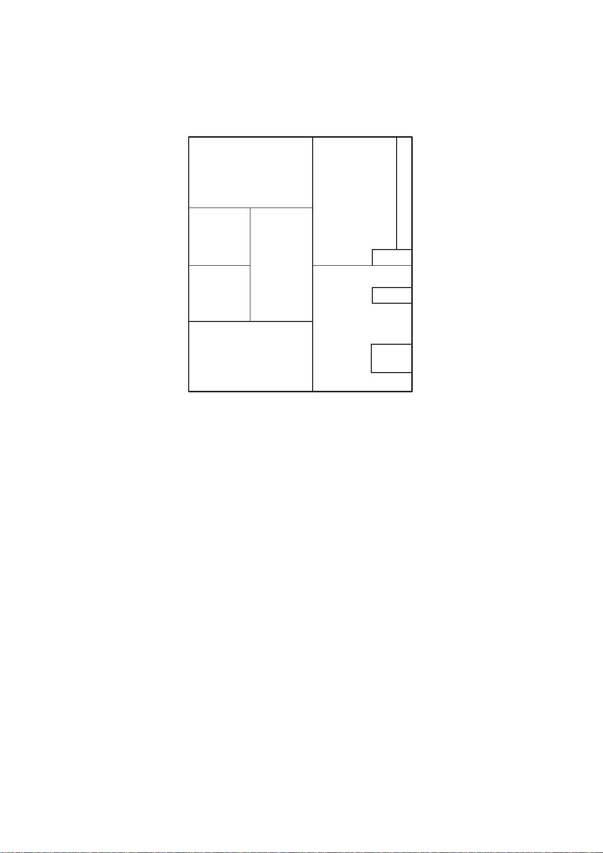
1.3 Voice Channel Codec Logic Diagram
+
–
Mic Preamp
20/0 dB Gain
Phantom Power
2.5 V/1.5 V @ 5 mA
MIC_AUDIO
MIC_BIAS
+
–
HSRXM
HSRXP
HSTX_OUT
+
–
HSTX_IN
Handset TX (Hybrid)
Handset RX (Hybrid)
+
–
HS_BUF
600-Ω Handset Out Buffer
0 dB or Mute
16-Bit
DAC
+
–
Line_Out PGA
12 to –36 dB
1.5 dB Noiseless Steps
31 Steps and Mute
+
–
Line_In PGA
12 to –36 dB
1.5 dB Noiseless Steps
31 Steps and Mute
16-Bit
ADC
+
–
+
–
+
–
60-Ω Pwr Spkr Buffer
0 dB or Mute
( Same Polarity)
SPKR_LEFT
TAPI_OUT
600-Ω
Out Buffer
0 dB or Mute
SPKR_RIGHT
HS_REF
HSRX_FB
M
I
X
E
R
–1
+
–
TAPI Preamp
20/0 dB Gain
TAPI_IN
2.5 V/1.5 V
2.5 V/1.5 V
2.5 V/1.5 V
2.5 V/1.5 V
2.5 V/1.5 V
Internal
2.5 V/1.5 V
Page 10
1–4
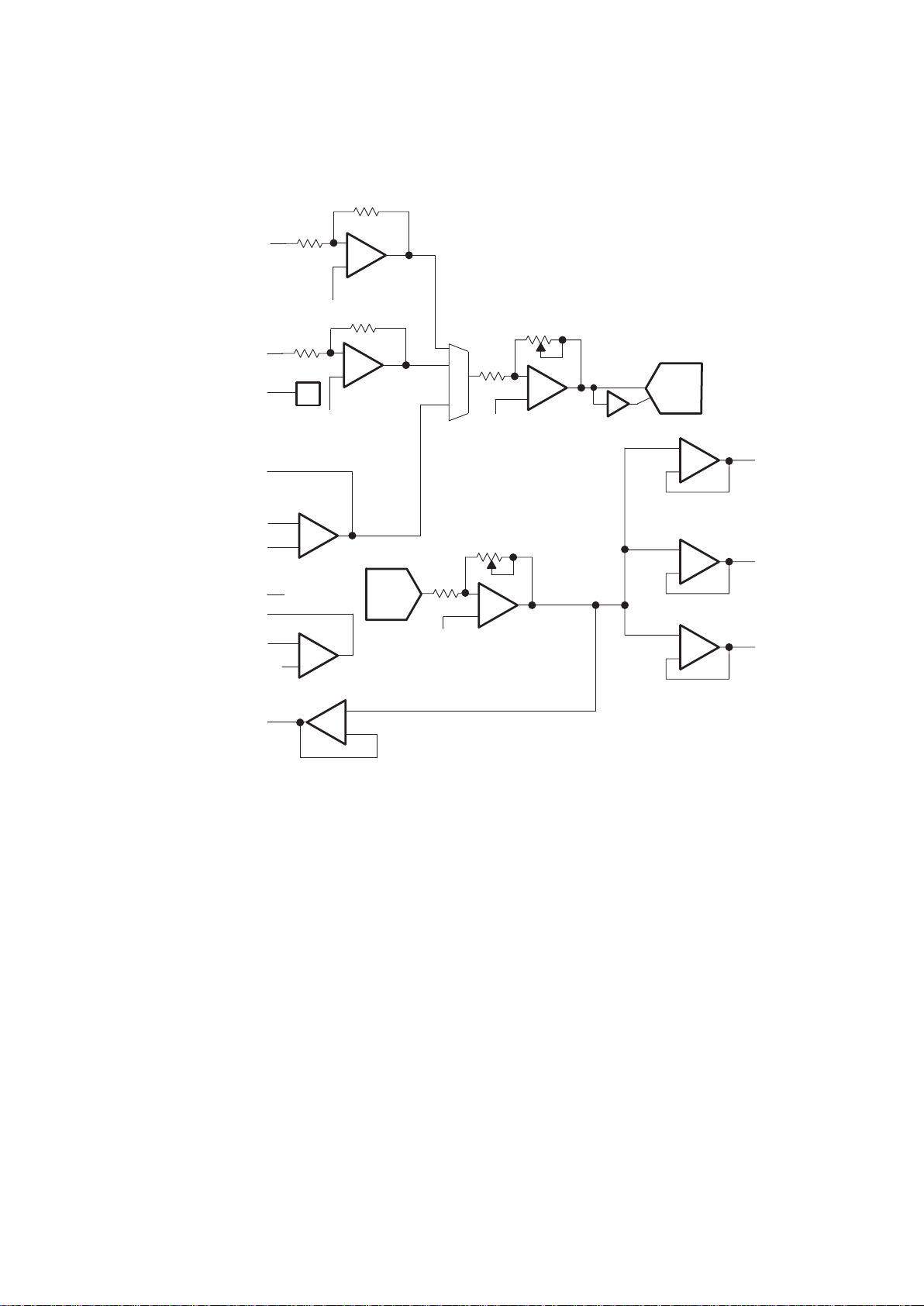
1.4 Data Channel Codec Logic Diagram
+
–
DTRX_FB
DTRXM
DTRXP
+
–
16-Bit
ADC
Data (Hybrid)
2.5 V/1.5 V
Data_In PGA
0/6/12/18 dB Gain
with Mute
+
–
Data (Hybrid)
DTTX_OUT
DTTX_IN
2.5 V/1.5 V
+
–
2.5 V/1.5 V
16-Bit
DAC
DT_BUF
+
–
+
–
0/–6/–12/–18 dB or Mute
600-Ω Data_Out PGA
8 Ω Speaker Buffer
0 dB or Mute
Mon_Out PGA
0-3-6-9-12 dB Gain
with Mute
MONOUTP
MONOUTM
2.5 V/1.5 V
@ 10 mA
M
U
X
–1
DT_REF
1.5 Terminal Assignments
1
2
3
4
5
6
7
8
9
10
39
40
41
42
43
44
45
46
47
48
VREFP_ADC
DAV
DD
DREFP_DAC
VAV
DD
VREFM_ADC
V
SS
DREFM_DAC
HSRXM
HSRXP
DTRXM
VAV
SS
VREFP_DAC
DAV
SS
DREFP_ADC
NC
DREFM_ADC
DTRX_FB
VREFM_DAC
HSRX_FB
NC
11
12
13
14
15
16
33
34
35
36
37
38
HSTX_OUT
DT_REF
DTTX_OUT
HS_REF
HSTX_IN
DTRXP
DTTX_IN
HS_BUF
NC
DT_BUF
NC
SI_SEL
1718 19 20 21 22 23 2425 26 27 282930 31 32
646362 61 60 59 58 5756 55 5453 52 51 50 49
NC–Make no external connection
FLSH_OUT
DT_FS
DT_DOUT
DV
DV
DD
SS
DT_SCLK
DT_DIN
DT_MCLK
VC_DIN
VC_DOUT
VC_MCLK
VC_SCLK
VC_FS
FLSH_IN
RESET
POR
NCNCMONOUTP
MVDDMONOUTM
MVSSNC
FIL T
MIC_BIAS
MIC_AUDIO
TEST1
TEST2
SPKR_RIGHT
SPKR_LEFT
TAPI_IN
TAPI_OUT
TLC320AD535C/I
Page 11
1–5
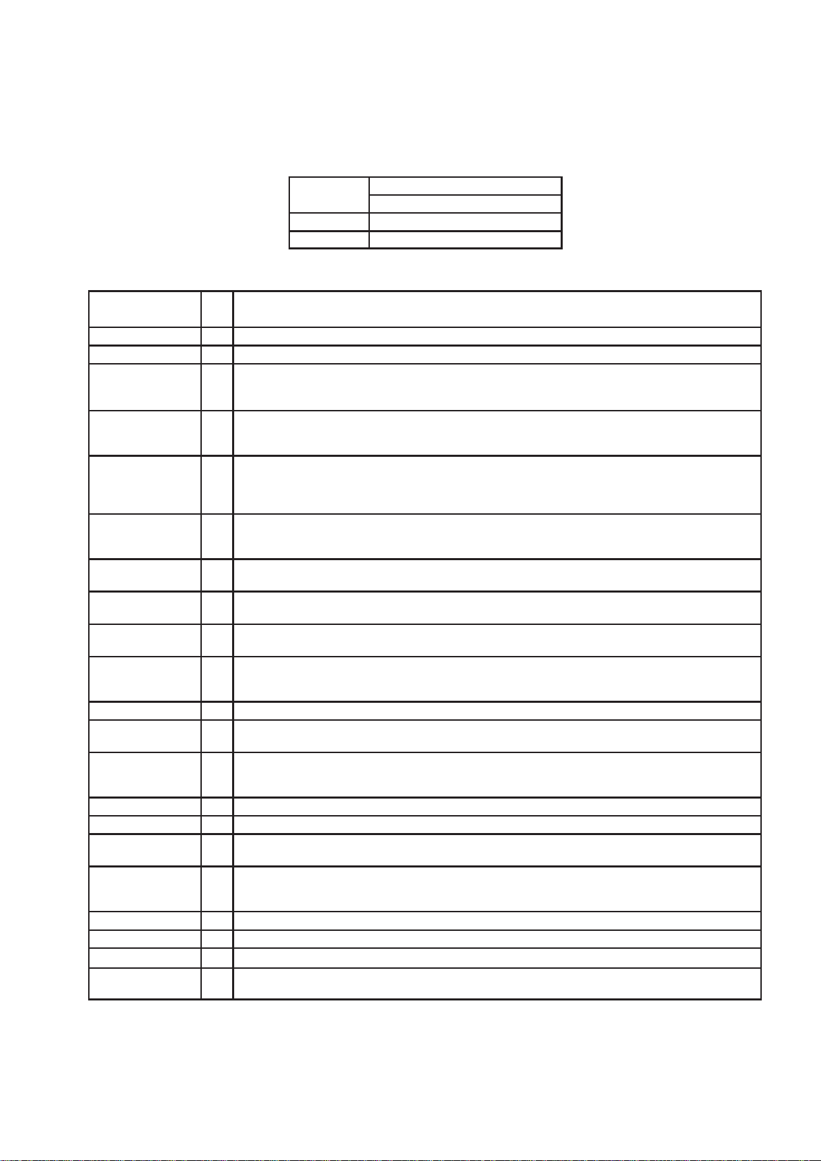
1.6 Ordering Information
PACKAGE
T
A
PLASTIC QUAD FLATPACK (PM)
0°C to 70°C TLC320AD535
–40°C to 85°C TLC320AD535I
1.7 Terminal Functions
TERMINAL
NAME NO.
I/O
DESCRIPTION
DAV
DD
2 I Data channel analog power supply (5 V/3.3 V)
DAV
SS
5 I Data channel analog ground
DREFM_ADC 7 O Data channel ADC voltage reference filter output. DREFM_ADC provides low-pass filtering for the internal
bandgap reference. The optimal ceramic capacitor value is 0.1 µF, which is connected between DREFM_ADC
and DREFP_ADC. The nominal DC voltage at this terminal is 0 V.
DREFM_DAC 4 O Data channel DAC voltage reference filter output. DREFM_DAC provides low-pass filtering for the internal
bandgap reference. The optimal ceramic capacitor value is 0.1 µF, which is connected between DREFM_DAC
and DREFP_DAC. The nominal dc voltage at this terminal is 0 V.
DREFP_ADC 6 O Data channel ADC voltage reference filter output. DREFP_ADC provides low-pass filtering for the internal
bandgap reference. The optimal ceramic capacitor value is 0.1 µF, which is connected between DREFM_ADC
and DREFP_ADC. The dc voltage at this terminal is 3.375 V at 5-V DAVDD supply and 2.25 V at 3.3-V DAV
DD
supply.
DREFP_DAC 3 O Data channel DAC voltage reference filter output. DREFP_DAC provides low-pass filtering for the internal
bandgap reference. The optimal ceramic capacitor value is 0.1 µF, which is connected between DREFM_DAC
and DREFP_DAC. The dc voltage at this terminal is 3.375 V at 5-DAVDD supply and 2.25 V at 3.3-DAVDD supply.
DT_BUF 15 O Data channel buffer amp analog output. DT_BUF is programmed for 0-dB gain or is muted using the control
registers. This output is normally fed to the DTTX_IN terminal through an input resistor.
DT_DIN 26 I Data channel digital data input. DT_DIN handles DAC input data as well as control register programming
information during the data channel frame sync interval and is synchronized to DT_SCLK.
DT_DOUT 22 O Data channel digital data output. Data channel ADC output bits are transmitted during the data channel frame
sync period that is synchronized to DT_SCLK. DT_DOUT is at high impedance when DT_FS is not activated.
DT_FS 21 O Data channel serial port frame sync signal. DT_FS signals the beginning of transmit for ADC data and receiving
of DAC data in the data channel. This signal can be active high (FS high mode) or active low (FS low mode)
depending on the voltage applied to SI_SEL (See Section 4,
Serial Communications
for more details).
DT_MCLK 27 I Data channel master clock input. All of the internal clocks for the data channel are derived from this clock.
DT_REF 12 O Handset amplifier reference voltage. The voltage at this pin is set at 2.5 V for a 5-V DA VDD supply and 1.5 V for
a 3.3-V DAVDD supply. The maximum source current at this terminal is 2.5 mA.
DTRX_FB 9 O Data channel receive path amplifier feedback node. DTRX_FB connects to the output of the data channel receive
path amplifier and allows a parallel resistor/capacitor to be placed in the amplifier feedback path for setting gain
and filter poles.
DTRXM 10 I Data channel receive path amplifier analog inverting input
DTRXP 11 I Data channel receive path amplifier analog noninverting input.
DT_SCLK 25 O Data channel shift clock signal. This signal clocks serial data into DT_DIN and out of DT_DOUT during the data
channel frame-sync interval. DT_SCLK = DT_MCLK/2
DTTX_IN 14 I Data channel transmit amplifier analog inverting input. This node is normally fed by the DT_BUF output through
an input resistor. The noninverting input of the amplifier is connected internally to 2.5 V for 5 V supply and 1.5
V for 3.3 V supply.
DTTX_OUT 13 O Data channel transmit amplifier analog output
DV
DD
24 I Digital power supply (5 V/3.3 V).
DV
SS
23 I Digital ground
FILT 57 O Bandgap filter node. FILT provides decoupling of the 3.375-V bandgap reference. The optimal capacitor value
is 0.1 µF (ceramic). This node should not be used as a voltage source.
Page 12

1–6
1.7 Terminal Functions (Continued)
TERMINAL
NAME NO.
I/O
DESCRIPTION
FLSH_IN 18 I External logic input. When brought low FLSH_IN enables the FLSH_OUT output.
FLSH_OUT 17 O Power output to write/erase flash EEPROM device (such as Intel 28F400B or AMD Am29F400). Outputs 5 V
(± 10%) at 45 mA maximum when FLSH_IN is brought low. FLSH_OUT does not go to a logic high state when
off. There is an internal NMOS pull down to maintain the specified voltage. An external pull down is not required.
HS_BUF 35 O Handset buffer amplifier analog output. HS_BUF can be programmed for 0-dB gain or muted using the control
registers. This output is normally fed to the HSTX_IN terminal through an input resistor.
HS_REF 38 O Handset amplifier reference voltage HS_REF is set at 2.5 V for 5-V supply and 1.5 V for 3.3-V supply. The
maximum source current at this terminal is 2.5 mA.
HSRX_FB 41 O Feedback node for handset receive path amplifier . HSRX_FB is connected to the output of the handset receive
path amplifier and allows a parallel resistor/capacitor to be placed in the amplifier feedback path for setting gain
and filter poles.
HSRXM 40 I Handset receive path amplifier analog inverting input
HSRXP 39 I Handset receive path amplifier analog noninverting input
HSTX_IN 36 I Handset transmit amplifier analog inverting input. This node is normally fed by the HSBUF output through an
input resistor. The noninverting input of the amplifier is connected internally to 2.5 V for 5 V supply and 1.5 V
for 3.3 V supply.
HSTX_OUT 37 O Handset transmit amplifier analog output
MIC_AUDIO 55 I Microphone preamplifier analog input. MIC_AUDIO can be programmed to add either 0-dB or 20-dB gain using
the control registers.
MIC_BIAS 56 O Output that provides 2.5 V/1.5 V bias for electret microphone. The maximum source current at this terminal
is 5 mA.
MONOUTM 60 O 8 Ω monitor speaker amplifier analog output. MONOUTM is set for 0-dB gain or is muted using the control
registers.
MONOUTP 62 O 8 Ω monitor speaker amplifier analog output. MONOUTP is set for 0-dB gain or is muted using the control
registers.
MV
DD
61 I Monitor amplifier supply (5 V/3.3 V)
MV
SS
59 I Monitor amplifier ground
NC All terminals marked NC should be left unconnected.
POR 20 O Power on reset signal. POR remains low while the 5-V supply at MVDD is below its threshold voltage and for
40 ms after it rises above the reset threshold.
RESET 19 I Codec device reset. RESET initializes all device internal registers to their default values. This signal is active
low.
SI_SEL 33 I Serial interface mode select. When SI_SEL is tied to DV
DD,
the serial port is in FS high mode. When SI_SEL
is tied to DVSS, the serial port is in FS low mode (See Section 4,
Serial Communications
for more details).
SPKR_LEFT 51 O Analog output from 60-Ω speaker line amplifier. SPKR_LEFT is set for 0-dB gain or is muted using the control
registers.
SPKR_RIGHT 52 O Analog output from 60-Ω speaker line amplifier . SPKR_RIGHT is set for 0-dB gain or is muted using the control
registers.
TAPI_IN 50 I Analog input to the TAPI (or sound card) preamplifier which can be programmed to add either 0 dB or 20 dB
gain via the control registers.
TAPI_OUT 49 O TAPI buffer amplifier analog output. This 600-Ω amplifier is set for 0-dB gain or is muted using the control
registers.
TEST1 54 I/O T est input/output port. TEST1 is for factory testing only and should be left unconnected.
TEST2 53 I/O T est input/output port. TEST2 is for factory testing only and should be left unconnected.
VAV
DD
48 I Voice channel analog power supply (5 V/3.3 V)
VAV
SS
45 I Voice channel analog ground
VC_DIN 28 I Voice channel digital data input. VC_DIN handles DAC input data as well as control register programming
information during the voice channel frame sync interval. VC_DIN is synchronized to VC_SCLK.
Page 13
1–7
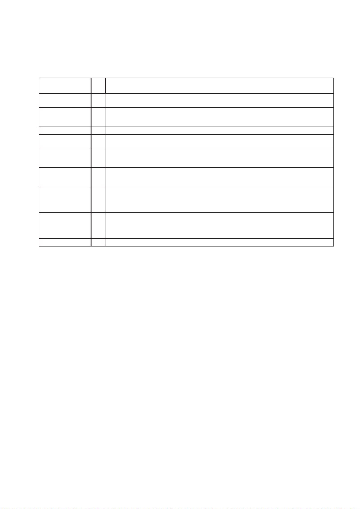
1.7 Terminal Functions (Continued)
TERMINAL
NAME NO.
I/O
DESCRIPTION
VC_DOUT 29 O Voice channel digital data output. Voice channel ADC output bits are transmitted during the voice channel frame
sync period synchronized to VC_SCLK. VC_DOUT is at high impedance when VC_FS is not activated.
VC_FS 32 O V oice channel serial port frame sync signal. VC_FS signals the beginning of transmit for ADC data and receive
of DAC data in the voice channel. This signal can be active high (FS high mode) or active low (FS low mode)
depending on the voltage applied to SI_SEL (see Section 4,
Serial Communication
for more details).
VC_MCLK 30 I Voice channel master clock input. All internal clocks for the voice channel are derived from this clock.
VC_SCLK 31 O Voice channel shift clock signal. VC_SCLK clocks serial data into VC_DIN and out of VC_DOUT during the
voice channel frame-sync interval. VC_SCLK = VC_MCLK/2
VREFM_ADC 46 O Voice channel ADC voltage reference filter output. VREFM_ADC provides low-pass filtering of the internal
bandgap reference. The optimal ceramic capacitor value is 0.1 µF , which is connected between VREFM_ADC
and VREFP_ADC. The nominal dc voltage at this terminal is 0 V.
VREFM_DAC 43 O Voice channel DAC voltage reference filter output. VREFM_DAC provides low-pass filtering of the internal
bandgap reference. The optimal ceramic capacitor value is 0.1 µF , which is connected between VREFM_DAC
and VREFP_DAC. The nominal dc voltage at this terminal is 0 V.
VREFP_ADC 47 O Voice channel ADC voltage reference filter output. VREFP_ADC provides low-pass filtering the internal
bandgap reference. The optimal ceramic capacitor value is 0.1 µF , which is connected between VREFM_ADC
and VREFP_ADC. The dc voltage at this terminal is 3.375 V with a 5-V V A VDD supply and 2.25 V with a 3.3-V
VAVDD supply.
VREFP_DAC 44 O Voice channel DAC voltage reference filter output. VREFP_DAC provides low-pass filtering the internal
bandgap reference. The optimal ceramic capacitor value is 0.1 µF , which is connected between VREFM_DAC
and VREFP_DAC. The dc voltage at this terminal is 3.375 V with a 5-V V A VDD supply and 2.25 V with a 3.3-V
VAVDD supply.
V
SS
1 I Internal substrate connection. VSS should be tied to either DAVSS or VAVSS for normal operation.
Page 14

1–8
Page 15

2–1
2 Functional Description
2.1 Device Requirements and System Overview
The TLC320AD535 device consists of two codec channels, a hybrid circuit with external resistors and capacitors for
setting gain and filter poles, two independent serial ports, and other miscellaneous logic functions.
2.2 Codec Functions
The codec portion of the TLC320AD535 device performs the functions required for two channels of analog-to-digital
conversion, digital-to-analog conversion, lowpass filtering, control of analog input and output gains, internal
oversampling coupled with internal decimation and interpolation, and two 16-bit serial port interfaces to the host
processor. The two serial ports operate independently and are capable of operating at different sample rates. The
maximum sample rate of either codec channel is 11.025 kHz.
2.3 Hybrid Functions
The hybrid circuitry in the data channel includes integrated amplifiers whose gains and filter pole frequencies are set
by external resistors and capacitors. This allows maximum flexibility to make adjustments for board variations and
international standards while providing integration of the function. The filter amplifier stages in the data channel are
followed by a programmable gain amplifier, which feeds 8-Ω differential speaker drivers for the AT41 call progress
monitor speakers. The monitor speaker driver can be programmed for 0-dB gain or muted through the control 2
register. The source for the monitor speaker input can be either the output of the amplified DAC output (Data_Out
PGA) or the ADC input signal through control register 1 (See
Appendix A
).
A 2.5 V/1.5 V reference voltage (DT_REF) is provided as a reference for the transformer. It is necessary to reference
to 2.5 V/1.5 V (rather than ground), since the amplifiers are powered off by single-rail supplies. DT_REF is 2.5 V when
DA V
DD
is 5 V and 1.5 V when DAVDD is 3.3 V.
2.4 Voice Channel Analog
The analog circuitry in the voice channel includes a microphone bias, which sources a maximum of 5 mA at 2.5 V/
1.5 V, and preamplifiers for the microphone, which can be selected for 0-dB or 20-dB gain. The device also has a
handset interface with receive and transmit amplifiers. These three inputs can be summed in any combination and
the result sent to a Line_In programmable gain amplifier (PGA) stage with gain range from 12 dB to –36 dB in 1.5
dB noiseless steps. This feeds the voice channel ADC. In the DAC path, the output of the DAC is sent to a Line-Out
PGA with gain range from 12 dB to –36 dB in 1.5 dB noiseless steps. This feeds both a 600-Ω TAPI output driver and
a 60-Ω mono speaker driver that can be muted or programmed for 0-dB gain. The time-out for noiseless gain change
or the maximum time the system can wait for a zero crossing of a signal before it will effect the gain change request
is approximately 9 ms.
2.5 Miscellaneous Logic and Other Circuitry
The logic functions include the circuitry required to implement two independent serial ports and control register
programming through secondary communication on those serial ports. There are five control registers that are
programmed during secondary communications from either the data channel serial port or the voice channel serial
port. These control registers set amplifier gains, choose multiplexer inputs, select loopback functions, and read the
ADC overflow flags. The device also includes a power-on reset (POR) circuit to monitor the 5-V MV
DD
power supply
in the system and provides a reset signal when the supply MVDD voltage drops below its threshold voltage. In addition,
there is a flash write enable (FWE) circuit that takes an external logic input and provides 40 mA of current to power
the write enable circuit of an external memory device. The flash write enable circuit is powered from the digital power
supply .
Page 16

2–2
Page 17

3–1
3 Codec Functional Description
3.1 Operating Frequencies
The TLC320AD535 is capable of supporting any sample rate up to the maximum sample rate of 1 1.025 kHz in either
the data channel or voice channel. The sample rate is set by the frequency of the codec master clock that is input
to the serial port for that channel.
The sampling (conversion) frequency is derived from the internally-generated codec master clock divider circuit by
the following equation:
fs+
Sampling (conversion) frequency
+ǒXX_MCLKń512
Ǔ
(1)
XX_SCLK+XX_MCLKń2
Where XX_MCLK refers to either the voice channel or data channel codec clock (VC_MCLK or DT_MCLK) fed to
the codec externally by the clock rate divider circuit. The clock rate divider circuit divides the system master clock
to obtain the necessary clock frequency to feed the codecs.
The inverse of the sampling frequency is the conversion period. The sample rates of the voice and data channels
can be set independently by their respective codec master clocks. The two codec channels can be sampled at
different rates simultaneously.
3.2 ADC Signal Channel
The input signals are amplified and filtered by on-chip buffers before being applied to their respective ADC input. In
the case of the voice channel, inputs from a microphone input and the handset input may be summed together before
being amplified/attenuated by the ADC line PGA. The ADC converts the signal into discrete output digital words in
2s-complement format, corresponding to the analog signal value at the sampling time. These 16-bit digital words,
representing sampled values of the analog input signal, are sent to the host through the serial port interface for their
respective channels. If the ADC reaches its maximum value, a control register flag is set. This overflow bit resides
at D0 in the data channel control register 2 or the voice channel control register 5. These bits can only be read from
their respective serial ports, and the overflow flag is cleared only if it is read through the voice channel serial port,
and similarly for the data channel. The ADC and DAC conversions are synchronous and phase-locked.
3.3 DAC Signal Channel
The DAC receives the 16-bit data words (2s complement) from the host through the serial port interface for each
channel. The data is converted to analog voltages by their respective sigma-delta DACs comprised of a digital
interpolation filter and a digital modulator. The outputs of the DACs are each then passed to internal low pass filters
to complete the signal reconstruction resulting in an analog signal. Those analog signals are then buffered and
amplified by an output driver capable of driving the required load. The gain of these output amplifiers is programmed
by the
+codec control registers, as shown in
Appendix A
.
3.4 Sigma-Delta ADC
Each ADC is an oversampling sigma-delta modulator. The ADC provides high resolution and low noise performance
using oversampling techniques and the noise shaping advantages of sigma-delta modulators.
3.5 Decimation Filter
Each decimation filter reduces the digital data rate to the sampling rate. This is accomplished by decimating with a
ratio equal to the oversampling ratio. The output of this filter is a 16-bit 2s-complement data word clocking at the
selected sample rate.
Page 18

3–2
3.6 Sigma-Delta DAC
Each DAC is an oversampling sigma-delta modulator. The DAC performs high-resolution, low-noise digital-to-analog
conversion using oversampling sigma-delta techniques.
3.7 Interpolation Filter
Each interpolation filter resamples the digital data at a rate of N times the incoming sample rate, where N is the
oversampling ratio. The high-speed data output from this filter is then applied to the sigma-delta DAC.
3.8 Analog and Digital Loopbacks
The test capabilities include an analog loopback and digital loopback. The loopbacks provide a means of testing the
ADC/DAC channels and are used for in-circuit system-level tests. The loopback feeds the ADC output to the DAC
input on the IC for each individual channel. The analog loopback functions test only the codec portions of the device
and do not include the hybrid amplifiers.
Analog loopback loops the DAC output back into the ADC input of the same channel. Digital loopback loops the ADC
output back into the DAC input of the respective channel. Analog loopback is enabled by setting the D4 bit in the
control register 1 for the data channel or control register 3 for the voice channel. Digital loopback is enabled by setting
the D5 bit high in control register 1 for the data channel or control register 3 for the voice channel.
3.9 Software Power Down
The software power down resets all internal counters, but leaves the contents of the programmable control registers
unchanged for the selected channel. The device has separate and independent software power down bits for the
voice and data channels. The software power down feature is invoked by setting the D6 bit high in control register
1 for the data channel or setting the D6 bit in control register 3 for the voice channel. There is no hardware power
down function in the TLC320AD535.
3.10 Reset Circuit
This circuit monitors the 5-V MVDD power supply coming into the device from the bus and asserts an active low
power-on-reset ( POR) signal whenever this supply voltage drops below its threshold voltage. The reset signal
remains low while the supply voltage is below the threshold voltage. It remains low for 40 ms (nominal) after the supply
voltage has risen above the reset threshold voltage. Once the voltage rises above the threshold, an internal counter
is activated and holds the POR signal low for an additional 40 ms (nominal). The signal then goes high and remains
high as long as the MV
DD
supply remains in the acceptable voltage range. This circuit is, in effect, on initial power
up of the device and POR is held low until the supply voltage rises above the threshold. In addition, a reset is triggered
if a transient spike of sufficient magnitude and duration occurs. The supply must drop below the threshold voltage
for a period of time greater than the delay time shown in the following table (delay time, MVDD to reset). If a spike
occurs that drops below the threshold, but the supply voltage returns above the threshold within the delay time, POR
remains in the high state.
Page 19

3–3
40 ms
20 µs
Detection of Threshold
Crossing as MV
DD
Goes High
20 µs
Detection of Threshold
Crossing as MV
DD
Goes Low
40 ms
Detection of Threshold
Crossing as MVDD Goes High
POR
0 V
MV
DD
V
(TO)
PARAMETER MIN NOM MAX UNIT
Delay time, MVDD to reset 10 20 40 µs
Delay time reset pulse (POR) 20 40 80 ms
Threshold voltage V
(TO)
5-V MV
DD
4.5 4.63 4.75 V
3.11 Test Module
The test module serves the purpose of facilitating design verification testing and simplifying factory production testing.
There are two input/output terminals (TEST1 and TEST2) dedicated to implementing the test functions. The function
of these terminals is for factory self-test only , and no connection (NC) should be made to either of these terminals.
Page 20

3–4
Page 21

4–1
4 Serial Communications
DT_DOUT, DT_DIN, DT_SCLK, and DT_FS are the serial communication signals for the data channel serial port,
while VC_DOUT, VC_DIN, VC_SCLK, and VC_FS are the serial communication signals for the voice channel serial
port. The digital output data from the ADC is taken from DT_DOUT (or VC_DOUT). The digital input data for the DAC
is applied to DT_DIN (or VC_DIN). The synchronization clock for the serial communication data and the frame-sync
is taken from DT_SCLK and VC_SCLK for the data and voice channels, respectively. The frame-sync pulse which
signals the beginning of the ADC and DAC data transfer interval is taken from DT_FS and VC_FS for the data and
voice channels, respectively .
For signal data transmitted from the ADC or to the DAC, a primary serial communication is used. A secondary
communication reads or writes words to the control registers, which control both the options and the circuit
configurations of the device.
The purpose of primary and secondary communications is to allow conversion data and control data to be transferred
across the same serial port. A primary transfer is always dedicated to conversion data. A secondary transfer is used
to set up or read the control register values described in
Appendix A, Programmable Register Set
. A primary transfer
occurs for every conversion period. A secondary transfer occurs only when requested. Secondary serial
communication is requested by software - D0 of the primary data input to DT_DIN for the data channel serial port or
to VC_DIN for the voice channel serial port. A secondary request can be made for the voice channel without making
a secondary request for the data channel, or vice versa. Control registers 1 and 2 can only be written to or read from
the data channel serial port. Control registers 3 through 6 can only be written to or read from the voice channel serial
port.
4.1 Primary Serial Communication
Primary serial communication transmits and receives conversion signal data. The DAC word length is 15 bits and
the last bit of the primary 16-bit serial communication word is a control bit used to request secondary serial
communication. For all serial communications, the most significant bit is transferred first. For the 16-bit ADC word,
D15 is the most significant bit, and D0 is the least significant bit. For the 15-bit DAC data word in a primary
communication, D15 is the most significant bit, D1 is the least significant bit, and D0 is used for the secondary
communication request control. All digital data values are in 2s-complement data format. Refer to Figure 4–1.
D15–D1 D0XX_DIN
D15–D0
D/A Data
XX_DOUT
Secondary
Communication Request
A/D Data
Figure 4–1. Primary Communication DIN and DOUT Data Format
Page 22

4–2
4.1.1 FS High Mode Primary Communication Timing
There are two possible modes for serial data transfer. One mode is the FS high mode which is selected by tying the
SI_SEL pin to DVDD. Figure 4–2 shows the timing relationship for XX_SCLK, XX_FS, XX_DOUT and XX_DIN in a
primary communication for either the voice or data channel when in FS high mode. The timing sequence for this
operation is as follows:
1. XX_FS is brought high and remains high for one XX_SCLK period, then goes low.
2. A 16-bit word is transmitted from the ADC (DT_DOUT and VC_DOUT) and a 16-bit word is received for DAC
conversion (DT_DIN and VC_DIN).
D15 D14 D13 D12 D11 D10 D9 D8 D7 D6 D5 D4 D3 D2 D1 D0
D15 D14 D13 D12 D11 D10 D9 D8 D7 D6 D5 D4 D3 D2 D1 D0
XX_FS
XX_SCLK
XX_DIN
XX_DOUT
Figure 4–2. FS High Mode Primary Serial Communication Timing
4.1.2 FS Low Mode Primary Communication Timing
The second possible serial interface mode is the FS low mode, which is selected by tying the SI_SEL pin to DVSS.
This mode differs from the FS high mode in that the frame sync signal (FS) is active low , data transfer starts on the
falling edge of XX_FS, and XX_FS remains low throughout the data transfer. Figure 4–3 shows the timing relationship
for XX_SCLK, XX_FS, XX_DOUT and XX_DIN in a primary communication for either the voice or data channel when
in FS low mode. The timing sequence for this operation is as follows:
1. XX_FS is brought low by the TLC320AD535.
2. A 16-bit word is transmitted from the ADC (DT_DOUT and VC_DOUT) and a 16-bit word is received for DAC
conversion (DT_DIN and VC_DIN).
3. XX_FS is brought high signaling the end of the data transfer.
D15 D14 D13 D12
D11
D10 D9 D8 D7 D6 D5 D4 D3 D2 D1 D0
D15 D14 D13 D12
D11 D10
D9 D8 D7 D6 D5 D4 D3 D2 D1 D0
XX_FS
XX_SCLK
XX_DIN
XX_DOUT
Figure 4–3. FS Low Mode Primary Serial Communication Timing
Page 23

4–3
4.2 Secondary Serial Communication
Secondary serial communication reads or writes 16-bit words that program both the options and the circuit
configurations of the device for either the voice channel or the data channel. Register programming always occurs
during secondary communication for that channel. Control registers 1 and 2 can only be written to or read from the
data channel serial port. Control registers 3 through 6 can only be written to or read from the voice channel serial port.
Four primary and secondary communication cycles are required to program the four voice channel registers. In the
same manner, two primary and secondary communication cycles are necessary to program the data channel control
registers. If the default value for a particular register is desired, then the register addressing can be omitted during
secondary communications. The NOOP (no operation) command addresses a pseudo-register, register 0, and no
register programming takes place during this secondary communication. This can be used for either the data channel
or the voice channel serial port.
During a secondary communication, a register is written to or read from. When writing a value to a register, the
DT_DIN (or VC_DIN) line contains the value to be written. The data returned on DT_DOUT (or VC_DOUT) is 00h.
The method for requesting a secondary communication is by asserting the least significant bit (D0) of DT_DIN (or
VC_DIN) high as shown in Table 4–1.
Table 4–1. Least-Significant-Bit Control Function
CONTROL BIT D0 CONTROL BIT FUNCTION
0 No secondary communication request
1 Secondary communication request
Figure 4–4 shows the data format XX_DIN and XX_DOUT during secondary communication.
D15–D0
–– –– 1 D12 D11 D10 D9 D8
D7–D0
Don’t Care
D15
XX_DIN
(Read)
–– –– 0 D12 D11 D10 D9 D8
D7–D0
Register Data
D15
XX_DIN
(Write)
Register AddressR/W
Register Data
D15–D8 D7–D0
AII 0
AII 0
XX_DOUT
(Read)
XX_DOUT
(Write)
Figure 4–4. Secondary Communication DIN and DOUT Data Format
Page 24

4–4
4.2.1 FS High Mode Secondary Communication Timing
On the rising edge of SCLK, coinciding with the falling edge of FS for that channel, D15–D0 is input serially to DT_DIN
(or VC_DIN), and D15–D0 is output serially on DT_DOUT (or VC_DOUT). If a secondary communication request is
made, FS goes high again 128 SCLKs after the beginning of the primary frame to signal the beginning of the
secondary frame one SCLK period later. See Figure 4–5.
XX_DIN
Data (D0=1) Register R/W Data (D0=0)
XX_FS
PSPP
Secondary Communication
Request
No Secondary
Communication Request
128 XX_SCLKs
Figure 4–5. FS Output During Software Secondary Serial Communication Request (FS High Mode)
4.2.2 FS Low Mode Secondary Communication Timing
On the falling edge of XX_FS for that channel, D15–D0 is input serially to XX_DIN and D15–D0 is output serially on
XX_DOUT . XX_FS remains low during the data transfer and then returns high. If a secondary communication request
is made, XX_FS goes low 128 SCLKs after the beginning of the primary frame to signal the beginning of the secondary
frame. See Figure 4–6.
XX_DIN
XX_FS
Data (D0=1) Register R/W Data (D0=0)
PSP
Secondary Communication
Request
No Secondary
Communication Request
128 XX_SCLKs
Figure 4–6. FS Output During Software Secondary Serial Communication Request (FS Low Mode)
Page 25

5–1
5 Specifications
5.1 Absolute Maximum Ratings Over Operating Free-Air Temperature Range
(Unless Otherwise Noted)
†
Supply voltage range, DVDD, AVDD (see Note 1) –0.3 V to 7 V. . . . . . . . . . . . . . . . . . . . . . . . . . . . . . . . . . . . . .
Output voltage range, all digital output signals –0.3 V to DV
DD
+ 0.3 V. . . . . . . . . . . . . . . . . . . . . . . . . . . . . . .
Input voltage range, all digital input signals –0.3 V to DV
DD
+ 0.3 V. . . . . . . . . . . . . . . . . . . . . . . . . . . . . . . . . .
Case temperature for 10 seconds: PM package 260°C. . . . . . . . . . . . . . . . . . . . . . . . . . . . . . . . . . . . . . . . . . . . .
Operating free-air temperature range, TA –40°C to 85°C. . . . . . . . . . . . . . . . . . . . . . . . . . . . . . . . . . . . . . . . . . .
Storage temperature range, T
stg
–65°C to 150°C. . . . . . . . . . . . . . . . . . . . . . . . . . . . . . . . . . . . . . . . . . . . . . . . . .
†
Stresses beyond those listed under “absolute maximum ratings” may cause permanent damage to the device. These are stress ratings only and
functional operation of the device at these or any other conditions beyond those indicated under “recommended operating conditions” is not
implied. Exposure to absolute-maximum-rated conditions for extended periods may affect device reliability.
NOTE 1: All voltage values are with respect to VSS.
5.2 Recommended Operating Conditions
MIN NOM MAX UNIT
pp
3.3-V supply 3 3.3 3.6
Suppl
y v
oltage, DAV
DD
,
VAV
DD
,
MV
DD
,
DV
DD
(see Note 2)
5-V supply 4.5 5 5.5
V
Analog signal peak-to-peak input voltage{, DT_RXM, DT_RXP, MIC_AUDIO, TAPI_IN,
3.3-V supply 2 V
gg g,_ ,_ , _ , _,
HS_RXM, HS_RXP, V
I(analog)
5-V supply 3 V
Differential output load resistance, T API_OUT, DT_BUF, HS_BUF, R
L
600 Ω
Differential output load resistance, MONOUTP, MONOUTM, R
L
8 Ω
Differential output load resistance, SPKR_RIGHT, SPKR_LEFT , R
L
60 Ω
Input impedance, MIC_AUDIO 50 kΩ
Master clock 5.645 MHz
Load capacitance, C
L
20 pF
ADC or DAC conversion rate 8 11.025 kHz
Operating free-air temperature, T
A
–40 85 °C
†
Preamplifier gain set to 0 dB
NOTE 2: Voltages at analog inputs and outputs and xVDD are with respect to the xVSS terminal.
5.3 Electrical Characteristics Over Operating Free-Air Temperature Range,
DV
DD
= 5 V/3.3 V, xAV
DD
= 5 V/3.3 V, MVDD=5 V/3.3 V
5.3.1 Digital Inputs and Outputs, fs = 8 kHz, Outputs Not Loaded
PARAMETER TEST CONDITIONS MIN TYP MAX UNIT
V
OH
High-level output voltage, any digital output IO = –360 µA 2.4 DVDD+0.5 V
V
OL
Low-level output voltage, any digital output IO = 2 mA DVSS–0.5 0.4 V
I
IH
High-level input current, any digital input VIH = 5 V 10 µA
I
IL
Low-level input current, any digital input VIL = 0.6 V 10 µA
C
i
Input capacitance, any digital input 10 pF
C
o
Output capacitance, any digital output 10 pF
I
I(lkg)
Input leakage current, any digital input 30 µA
I
OZ
Output leakage current, any digital output 30 µA
Page 26

5–2
5.3.2 ADC Channel, fs = 8 kHz (see Note 3)
PARAMETER TEST CONDITIONS MIN TYP MAX UNIT
0 to 300 Hz –0.5 0.2
300 Hz to 3 kHz –0.5 0.25
3.3 kHz –0.5 0.3
Filter gain relative to gain at 1020 H
z
3.6 kHz –3
dB
4 kHz –35
≥ 4.4 kHz –74
NOTE 3: The filter gain outside of the passband is measured with respect to the gain at 1020 Hz. The analog input test signal is a sine wave with
0 dB = 3 V
I(PP)
at 5-V supply and 0 dB = 2 V
I(PP)
at 3.3-V supply voltage as the reference level for the ADC analog input signal. The
–3-dB passband is 0 to 3600 Hz for an 8-kHz sample rate. This pass-band scales linearly with the sample rate.
5.3.3 ADC Dynamic Performance, fs = 8 kHz
5.3.3.1 ADC Signal-to-Noise (see Note 4)
PARAMETER TEST CONDITIONS MIN TYP MAX UNIT
VI = –1 dB 75 80
Signal-to-noise ratio (SNR)
VI = –9 dB 67 72
dB
VI = –40 dB 36 36
NOTE 4: The test condition is a 1020-Hz input signal with an 8-kHz conversion rate. Input and output are referred to 2.5 V for 5-V supply and
1.5 V for 3.3-V supply. The output configuration is in a 3.3 V single ended mode.
5.3.3.2 ADC Signal-to-Distortion (see Note 4)
PARAMETER TEST CONDITIONS MIN TYP MAX UNIT
VI = –3 dB 73 78
Signal-to-total harmonic distortion (THD)
VI = –9 dB 77 82
dB
VI = –40 dB 56 61
NOTE 4: The test condition is a 1020-Hz input signal with an 8-kHz conversion rate. Input and output are referred to 2.5 V for 5-V supply and
1.5 V for 3.3-V supply. The output configuration is in a 3.3 V single ended mode.
5.3.3.3 ADC Signal-to-Distortion + Noise (see Note 4)
PARAMETER TEST CONDITIONS MIN TYP MAX UNIT
VI = –3dB 72 77
Signal-to-total harmonic distortion + noise (THD + N)
VI = –9 dB 68 73
dB
VI = –40 dB 37 42
NOTE 4: The test condition is a 1020-Hz input signal with an 8-kHz conversion rate. Input and output are referred to 2.5 V for 5-V supply and
1.5 V for 3.3-V supply. The output configuration is in a 3.3 V single ended mode.
Page 27

5–3
5.3.4 ADC Characteristics
PARAMETER TEST CONDITIONS MIN TYP MAX UNIT
V
I(PP)
Peak-input voltage, TAPI_IN, MIC_AUDIO Preamp gain = 0 dB 3 V
Dynamic range 80 dB
Intrachannel isolation 85 dB
E
G
Gain error VI = –1 dB at 1020 kHz ±0.6 dB
E
O(ADC)
ADC channel offset error including hybrid amplifiers
With a 0.1-µF capacitor between
CAP_D and DTRX_FB
5 mV
E
O(ADC)
ADC channel offset error including hybrid amplifiers
With no capacitor between CAP_D
and DTRX_FB
20 mV
Idle channel noise (on-chip reference) 26 75 µV rms
Channel delay 17/f
s
s
5.3.5 DAC Channel, fs = 8 kHz (see Note 5)
PARAMETER TEST CONDITIONS MIN TYP MAX UNIT
0 to 300 Hz –0.5 0.3
300 Hz to 3 kHz –0.25 0.25
3.3 kHz –0.35 0.3
Filter gain relative to gain at 1020 H
z
3.6 kHz –3
dB
4 kHz –35
≥ 4.4 kHz –70
NOTE 5: The filter gain outside of the passband is measured with respect to the gain at 1020 Hz. The input signal is the digital equivalent of a
sine wave (digital full scale = 0 dB). The –3 dB passband is 0 to 3600 Hz for an 8-kHz sample rate. This pass band scales linearly with
the sample rate.
5.3.6 DAC Dynamic Performance
5.3.6.1 DAC Signal-to-Noise (see Note 6)
PARAMETER TEST CONDITIONS MIN TYP MAX UNIT
VI = 0 dB 71 76
Signal-to-noise ratio (SNR)
VI = –9 dB 62 67
dB
VI = –40 dB 31 36
NOTE 6: The test condition is a 1020-Hz input signal with an 8-kHz conversion rate. The output configuration is in a 3.3 V single ended mode.
5.3.6.2 DAC Signal-to-Distortion (see Note 6)
PARAMETER TEST CONDITIONS MIN TYP MAX UNIT
VI = –3 dB 78 83
Signal-to-total harmonic distortion (THD)
VI = –9 dB 70 75
dB
VI = –40 dB 56 61
NOTE 6: The test condition is a 1020-Hz input signal with an 8-kHz conversion rate. The output configuration is in a 3.3 V single ended mode.
5.3.6.3 DAC Signal-to-Distortion + Noise (see Note 6)
PARAMETER TEST CONDITIONS MIN TYP MAX UNIT
VI = –3 dB 69 74
Signal-to-total harmonic distortion + noise (THD + N)
VI = –9 dB 63 68
dB
VI = –40 dB 30 35
NOTE 6: The test condition is a 1020-Hz input signal with an 8-kHz conversion rate. The output configuration is in a 3.3 V single ended mode.
Page 28

5–4
5.3.7 DAC Characteristics
PARAMETER TEST CONDITIONS MIN TYP MAX UNIT
Dynamic range 79 dB
Intrachannel isolation 85 dB
E
G
Gain error VI = –1 dB at 1020 kHz ±0.7 dB
Idle channel narrow-band noise 0 kHz to 4 kHz (see Note 7) 125 µV rms
Channel delay 18/f
s
s
V
OO
Output offset voltage, HS_BUF, DT_BUF DIN = All zeros 25 mV
p
Differential with respect to MVDD/2
p
5 V –1.78 1.78
VOAnalog output voltage, MONOUTP-MONOUTM
and full-scale digital input
(see Note 8)
3.3 V –1.2 1.2
V
Analog output voltage, TAPI_OUT, SPKR_LEFT, Single-ended with respect to
5 V –2 2 V
V
O
gg
SPKR_RIGHT
g
HS_REF and full-scale digital input
3.3 V –1.5 1.5 V
NOTES: 7. The conversion rate is 8 kHz.
8. This amplifier should only be used in differential mode. Common mode: 2.5 V in 5 V supply and 1.5 V in 3.3 V supply.
5.3.8 Logic DC Electrical Characteristics
PARAMETER MIN TYP MAX UNIT
V
IL
Low-level input voltage –0.3 1.5 V
V
IH
High-level input voltage 2.4 DV
DD+
0.3 V
I
I(lkg)
Input leakage current 10 µA
I
O(lkg)
Output leakage current 10 µA
V
OH
High-level output voltage at rated load current 2.4 DVDD–0.5 V
V
OL
Low-level output voltage at rated load current DVSS–0.5 0.4 V
5.3.9 Power Supply Rejection (see Note 9)
PARAMETER TEST CONDITIONS MIN TYP MAX UNIT
V
DD1
Supply-voltage rejection ratio, ADC channel DAVDD and VAV
DD
fi = 0 to fs/2 50
V
DD2
Supply-voltage rejection ratio, ADC channel, DV
DD
fi = 0 to fs/2 40
V
DD3
Supply-voltage rejection ratio, DAC channel, DAVDD and VAV
DD
fi = 0 to fs/2 50
dB
V
DD4
Supply-voltage rejection ratio, DAC channel, DV
DD
fi = 0 to 30 kHz 50
NOTE 9: Power supply rejection measurements are made with both the ADC and the DAC channels idle and a 200 mV peak-to-peak signal
applied to the appropriate supply .
5.3.10 Power Supply
PARAMETER TEST CONDITIONS MIN TYP MAX UNIT
I
DD(analog)
Codec power supply current, analog (including hybrid and drivers) Operating 40 60 mA
I
DD(digital)
Codec power supply current, digital Operating 10 mA
I
DD(monitor)
Power supply current, 8 Ω monitor speaker driver Operating 135 315 mA
Page 29

5–5
5.3.11 Reset Circuit
PARAMETER TEST CONDITIONS MIN TYP MAX UNIT
V
(TO)
Reset threshold voltage TA= –40°C to 85°C for 5 V 4.50 4.75 V
V
OL
POR output low-level voltage I
(SINK)
= 1.2 mA 0.3 V
V
OL
POR output low-level voltage I
(SINK)
= 3.2 mA 0.4 V
V
OH
POR output high-level voltage I = –500 µA 0.8 DV
DD
V
t
d(RPD)
POR low delay time after threshold exceeded 20 40 80 ms
t
d(RDD)
Delay time after threshold crossed before POR activates 10 20 40 µs
5.3.12 Flash Write Enable Circuit
PARAMETER TEST CONDITIONS MIN TYP MAX UNIT
p
FLSH_IN low (5 V supply) 4.5 5 5.5
V
OH(FLSH_OUT)
Output high-level voltage, FLSH_OUT
FLSH_IN low (3.3 V supply) 2.5 3 3.5
V
V
OL(FLSH_OUT)
Output low-level voltage, FLSH_OUT FLSH_IN high 0 1.5 V
p
FLSH_IN low (5 V supply) 40 45 mA
I
O(FLSH_OUT)
Out ut current, FLSH_OUT
FLSH_IN low (3.3 V supply) 25 mA
5.3.13 8-Ω Drive
PARAMETER TEST CONDITIONS MIN TYP MAX UNIT
Output gain when PGA gain is mute –96
Output gain when PGA gain is 0 dB
–12 dB (input)
–1.5 0.7 1.5
dB
Output gain when PGA gain is 12 dB 10.5 12.5 13.5
5.4 Timing Characteristics (see Parameter Measurement Information)
5.4.1 Timing Requirements
PARAMETER MIN TYP MAX UNIT
t
d1
Delay time, XX_SCLK↑ to XX_FS↓ 0 ns
t
su1
Setup time, XX_DIN, before XX_SCLK low 25 ns
t
h1
Hold time, XX_DIN, after XX_SCLK high 20 ns
t
d3
Delay time, XX_MCLK↓ to XX_SCLK↑ 50 ns
t
wH
Pulse duration, XX_MCLK high 32 ns
t
wL
Pulse duration, XX_MCLK low 20 ns
t
pW
RESET input pulse width 10MCLKS ns
5.4.2 Switching Characteristics
PARAMETER TEST CONDITIONS MIN TYP MAX
UNIT
t
d2
Delay time, XX_SLCK↑ to XX_DOUT 20
t
en1
Enable time, XX_FS↓ to XX_DOUT
CL = 20 pF
25
ns
t
dis1
Disable time, XX_FS↑ to XX_DOUT Hi-Z 20
Page 30

5–6
5.5 Parameter Measurement Information
t
wH
t
d3
t
wL
t
d1
t
d2
t
en1
t
dis1
D15 D14
D15 D14
t
su1
t
h1
XX_MCLK
XX_SCLK
XX_FS
XX_DOUT
XX_DIN
Figure 5–1. Serial Communication Timing for FS High Mode
–40
0.8 1.6 2.4 3.2 4 4.8
–20
0
5.6 6.4 7.2
–60
–100
– 120
–80
fI – Input Frequency – kHz
Attenuation – dB
Figure 5–2. ADC Decimation Filter Response
Page 31

5–7
0.6
0.4 0.8 1.2 1.6 2 2.4
0.8
2.8 3.2
0.4
–0.4
–0.6
–0.2
fI – Input Frequency – kHz
Attenuation – dB
0.2
0
–0.8
Figure 5–3. ADC Decimation Filter Passband Ripple
–40
0.8 1.6 2.4 3.2 4 4.8
–20
0
5.6 6.4 7.2
–60
–100
– 120
–80
fI – Input Frequency – kHz
Attenuation – dB
Figure 5–4. DAC Interpolation Filter Response
Page 32

5–8
0.6
0.4 0.8 1.2 1.6 2 2.4
0.8
2.8 3.2
0.4
–0.4
–0.6
–0.2
fI – Input Frequency – kHz
Attenuation – dB
0.2
0
–0.8
Figure 5–5. DAC Interpolation Filter Passband Ripple
Page 33

6–1
6 Application Information
Data
Channel
Serial
Port
Data Channel
Codec
H
Y
B
R
I
D
A
M
P
DRVR
DRVR
BIAS/
AMPL
Voice Channel
Codec
Voice
Channel
Serial
Port
Power
Reset
Circuit
Flash
Write
Enable
Control
Logic
TAPI I/F
SPKR
AT41
SPKR
Matching
Network
POTS
Headset I/F
MIC
Figure 6–1. Functional Block of a Typical Application
Page 34

6–2
+
–
Mic Preamp
20/0 dB Gain
Phantom Power
2.5 V/1.5 V @ 5 mA
MIC_AUDIO
MIC_BIAS
+
–
HSRXP
HSTX_OUT
+
–
HSTX_IN
Handset TX (Hybrid)
Handset RX (Hybrid)
+
–
HS_BUF
600 Ω Handset Out Buffer
0 dB or Mute
16-Bit
DAC
+
–
Line_Out PGA 12 to –36 dB
1.5 dB Noiseless Steps
31 Steps and Mute
+
–
Line_In PGA 12 to –36 dB
1.5 dB Noiseless Steps
31 Steps and Mute
16-Bit
ADC
+
–
60 Ω Pwr Spkr Buffer
0 dB or Mute
( Same Polarity)
SPKR_LEFT
TAPI_OUT
600 Ω TPI Out Buffer
0 dB or Mute
SPKR_RIGHT
HS_REF
HSRX_FB
Voice Channel Codec
0.33 µF
2.2 kΩ
††
††
††
†
†
†
†
2.2 µF
2.2 µF
2.2 µF
–1
From
Hand Set
HSRXM
†
Required to meet communication standards
+
–
+
–
M
I
X
E
R
+
–
TAPI Preamp
20/0 dB Gain
TAPI_IN
2.5 V/1.5 V
2.5 V/1.5 V
2.5 V/1.5 V
2.5 V/1.5 V
2.5 V/1.5 V
2.5 V/1.5 V
Internal
Figure 6–2. Voice Channel Codec Typical Application
Page 35

6–3
DTRXM
DTRXP
+
–
16-Bit
ADC
Data (Hybrid)
2.5 V/1.5 V
Data_In PGA
0/6/12/18 dB Gain
With Mute
Data (Hybrid)
DTTX_OUT
DTTX_IN
+
–
16-Bit
DAC
DT_BUF
+
–
+
–
0/-6/-12/-18 dB or Mute
600 Ω Data_Out PGA
8 Ω Speaker Buffer
0 dB or Mute
Mon_Out PGA
0-3-6-9-12 dB Gain
with Mute
MONOUTP
MONOUTM
M
U
X
+
–
DTREF (2.5 V @ 10 mA)
+
–
††
††
††
†
†
†
†
AT41
T1
Primary
(Line)
†
Required to meet communication standards
–1
2.5 V/1.5 V
2.5 V/1.5 V
2.5 V/1.5 V
Figure 6–3. Data Channel Codec Typical Application
Page 36

6–4
Page 37

A–1
Appendix A
Programmable Register Set
Bits D12–D8 in a secondary serial communication comprise the address of the register that is written with data carried
in bits D7–D0. D13 determines a read or write cycle to the addressed register. When low (0), a write cycle is selected.
Table A–1 shows the register map.
T able A–1. Register Map
REGISTER NO. D15 D14 D13 D12 D11 D10 D9 D8 REGISTER NAME
0 0 0 R/W 0 0 0 0 0 No operation
1 0 0 R/W 0 0 0 0 1 Control 1
2 0 0 R/W 0 0 0 1 0 Control 2
3 0 0 R/W 0 0 0 1 1 Control 3
4 0 0 R/W 0 0 1 0 0 Control 4
5 0 0 R/W 0 0 1 0 1 Control 5
6 0 0 R/W 0 0 1 1 0 Control 6
Table A–2. Control Register 1, Data Channel Control
D7 D6 D5 D4†D3 D2 D1 D0 DESCRIPTION
1 — — 0 — — — — Software reset for data channel asserted
0 — — 0 — — — — Software reset for data channel not asserted
— 1 — 0 — — — — S/W power down for data channel enabled
— 0 — 0 — — — — S/W power down for data channel disabled
— — 1 0 — — — — Data channel digital loopback asserted
— — 0 0 — — — — Data channel digital loopback not asserted
— — — 0 1 — — — Select data_in PGA for monitor amp input
— — — 0 0 — — — Select DAC output for monitor amp input
— — — 0 — 1 — 1 Monitor amp PGA gain = 12 dB
— — — 0 — 1 0 Monitor amp PGA gain = 9 dB
— — — 0 — 0 1 1 Monitor amp PGA gain = 6 dB
— — — 0 — 0 1 0 Monitor amp PGA gain = 3 dB
— — — 0 — 0 0 1 Monitor amp PGA gain = 0 dB
— — — 0 — 0 0 0 Monitor amp PGA gain = mute
†
D4 = reserved
Default value: 00000000
Page 38

A–2
Table A–3. Control Register 2, Data Channel Control
D7 D6 D5 D4 D3 D2 D1 D0 DESCRIPTION
1 0 0 — — — — — Data in (DTRX) PGA gain = mute
0 1 1 — — — — — Data in (DTRX) PGA gain = 18 dB
0 1 0 — — — — — Data in (DTRX) PGA gain = 12 dB
0 0 1 — — — — — Data in (DTRX) PGA gain = 6 dB
0 0 0 — — — — — Data in (DTRX) PGA gain = 0 dB
— — — 1 0 0 — — DAC data out PGA gain = mute
— — — 0 1 1 — — DAC data out PGA gain = –18 dB
— — — 0 1 0 — — DAC data out PGA gain = –12 dB
— — — 0 0 1 — — DAC data out PGA gain = –6 dB
— — — 0 0 0 — — DAC data out PGA gain = 0 dB
— — — — — — 1 — 8 ohm monitor speaker driver gain = 0 dB
— — — — — — 0 — 8 ohm monitor speaker driver gain = mute
— — — — — — — X Data channel ADC overflow indicator: ← 1 = overflow
Default value: 00000000
Table A–4. Control Register 3, Voice Channel Control
D7 D6 D5 D4 D3 D2 D1 D0 DESCRIPTION
1 — — — — — — — Voice channel software reset
0 — — — — — — — Voice channel software reset not asserted
— 1 — — — — — — Software power down for voice channel enabled
— 0 — — — — — — Software power down for voice channel disabled
— — 1 — — — — — Voice channel digital loopback
— — 0 — — — — — Voice channel digital loopback not asserted
— — — 1 — — — — Voice channel digital loopback
— — — 0 — — — — Voice channel digital loopback not asserted
— — — — 1 — — — TAPI preamp seleted for ADC input
— — — — 0 — — — TAPI preamp not selected for ADC input
— — — — — 1 — — Microphone preamp selected for ADC input
— — — — — 0 — — Microphone preamp not selected for ADC input
— — — — — — 1 — Handset preamp not selected for ADC input
— — — — — — 0 — Handset preamp selected for ADC input
— — — — — — — 1 TAPI output buffer gain = mute
— — — — — — — 0 TAPI output buffer gain = 0 dB
Default value: 00000000
Page 39

A–3
Table A–5. Control Register 4, Voice Channel Control
D7 D6 D5 D4 D3 D2 D1 D0 DESCRIPTION
1 — — — — — — — TAPI_IN preamp gain = 20 dB
0 — — — — — — — TAPI preamp gain = 0 dB
— 1 — — — — — — Microphone preamp gain = 20 dB
— 0 — — — — — — Microphone preamp gain = 0 dB
— — 1 1 0 0 0 0 Voice ADC input PGA gain = mute
— — 1 0 0 0 0 1 Voice ADC input PGA gain = 12 dB
— — 1 0 0 0 0 0 Voice ADC input PGA gain = 10.5 dB
— — 0 1 1 1 1 1 Voice ADC input PGA gain = 9 dB
— — 0 1 1 1 1 0 Voice ADC input PGA gain = 7.5 dB
— — 0 1 1 1 0 1 Voice ADC input PGA gain = 6 dB
— — 0 1 1 1 0 0 Voice ADC input PGA gain = 4.5 dB
— — 0 1 1 0 1 1 Voice ADC input PGA gain = 3 dB
— — 0 1 1 0 1 0 Voice ADC input PGA gain = 1.5 dB
— — 0 1 1 0 0 1 Voice ADC input PGA gain = 0 dB
— — 0 1 1 0 0 0 Voice ADC input PGA gain = –1.5 dB
— — 0 1 0 1 1 1 Voice ADC input PGA gain = –3 dB
— — 0 1 0 1 1 0 Voice ADC input PGA gain = –4.5 dB
— — 0 1 0 1 0 1 Voice ADC input PGA gain = –6 dB
— — 0 1 0 1 0 0 Voice ADC input PGA gain = –7.5 dB
— — 0 1 0 0 1 1 Voice ADC input PGA gain = –9 dB
— — 0 1 0 0 1 0 Voice ADC input PGA gain = –10.5 dB
— — 0 1 0 0 0 1 Voice ADC input PGA gain = –12 dB
— — 0 1 0 0 0 0 Voice ADC input PGA gain = –13.5 dB
— — 0 0 1 1 1 1 Voice ADC input PGA gain = –15 dB
— — 0 0 1 1 1 0 Voice ADC input PGA gain = –16.5 dB
— — 0 0 1 1 0 1 Voice ADC input PGA gain = –18 dB
— — 0 0 1 1 0 0 Voice ADC input PGA gain = –19.5 dB
— — 0 0 1 0 1 1 Voice ADC input PGA gain = –21 dB
— — 0 0 1 0 1 0 Voice ADC input PGA gain = –22.5 dB
— — 0 0 1 0 0 1 Voice ADC input PGA gain = –24 dB
— — 0 0 1 0 0 0 Voice ADC input PGA gain = –25.5 dB
— — 0 0 0 1 1 1 Voice ADC input PGA gain = –27 dB
— — 0 0 0 1 1 0 Voice ADC input PGA gain = –28.5 dB
— — 0 0 0 1 0 1 Voice ADC input PGA gain = –30 dB
— — 0 0 0 1 0 0 Voice ADC input PGA gain = –31.5 dB
— — 0 0 0 0 1 1 Voice ADC input PGA gain = –33 dB
— — 0 0 0 0 1 0 Voice ADC input PGA gain = –34.5 dB
— — 0 0 0 0 0 1 Voice ADC input PGA gain = –36 dB
— — 0 0 0 0 0 0 Voice ADC input PGA gain = 0 dB
Default value: 00000000
Page 40

A–4
Table A–6. Control Register 5, Voice Channel Control
D7 D6 D5 D4 D3 D2 D1 D0 DESCRIPTION
1 1 0 0 0 0 — — Voice DAC output PGA gain = mute
1 0 0 0 0 1 — — Voice DAC output PGA gain = 12 dB
1 0 0 0 0 0 — — Voice DAC output PGA gain = 10.5 dB
0 1 1 1 1 1 — — Voice DAC output PGA gain = 9 dB
0 1 1 1 1 0 — — Voice DAC output PGA gain = 7.5 dB
0 1 1 1 0 1 — — Voice DAC output PGA gain = 6 dB
0 1 1 1 0 0 — — Voice DAC output PGA gain = 4.5 dB
0 1 1 0 1 1 — — Voice DAC output PGA gain = 3 dB
0 1 1 0 1 0 — — Voice DAC output PGA gain = 1.5 dB
0 1 1 0 0 1 — — Voice DAC output PGA gain = 0 dB
0 1 1 0 0 0 — — Voice DAC output PGA gain = –1.5 dB
0 1 0 1 1 1 — — Voice DAC output PGA gain = –3 dB
0 1 0 1 1 0 — — Voice DAC output PGA gain = –4.5 dB
0 1 0 1 0 1 — — Voice DAC output PGA gain = –6 dB
0 1 0 1 0 0 — — Voice DAC output PGA gain = –7.5 dB
0 1 0 0 1 1 — — Voice DAC output PGA gain = –9 dB
0 1 0 0 1 0 — — Voice DAC output PGA gain = –10.5 dB
0 1 0 0 0 1 — — Voice DAC output PGA gain = –12 dB
0 1 0 0 0 0 — — Voice DAC output PGA gain = –13.5 dB
0 0 1 1 1 1 — — Voice DAC output PGA gain = –15 dB
0 0 1 1 1 0 — — Voice DAC output PGA gain = –16.5 dB
0 0 1 1 0 1 — — Voice DAC output PGA gain = –18 dB
0 0 1 1 0 0 — — Voice DAC output PGA gain = –19.5 dB
0 0 1 0 1 1 — — Voice DAC output PGA gain = –21 dB
0 0 1 0 0 1 — — Voice DAC output PGA gain = –24 dB
0 0 1 0 0 0 — — Voice DAC output PGA gain = –25.5 dB
0 0 0 1 1 1 — — Voice DAC output PGA gain = –27 dB
0 0 0 1 1 0 — — Voice DAC output PGA gain = –28.5 dB
0 0 0 1 0 1 — — Voice DAC output PGA gain = –30 dB
0 0 0 1 0 0 — — Voice DAC output PGA gain = –31.5 dB
0 0 0 0 1 1 — — Voice DAC output PGA gain = –33 dB
0 0 0 0 1 0 — — Voice DAC output PGA gain = –34.5 dB
0 0 0 0 0 1 — — Voice DAC output PGA gain = –36 dB
0 0 0 0 0 0 — — Voice DAC output PGA gain = 0 dB
— — — — — — 1 — 60 Ω Spkr_L/R buffer gain = 0 dB
— — — — — — 0 — 60 Ω Spkr_L/R buffer gain = mute
— — — — — — — X Voice channel ADC overflow: 1 = overflow
Default value: 00000000
Table A–7. Control Register 6, Voice Channel Control
D7 D6 D5 D4 D3 D2 D1 D0 DESCRIPTION
1 — — — — — — — Handset out buffer gain = mute
0 — — — — — — — Handset out buffer gain = 0 dB
— X X X X X X X Reserved
Default value: 00000000
Page 41

B–1
Appendix B
Mechanical Data
PM (S-PQFP-G64)
PLASTIC QUAD FLATPACK
4040152/C 11/96
32
17
0,13 NOM
0,25
0,45
0,75
Seating Plane
0,05 MIN
Gage Plane
0,27
33
16
48
1
0,17
49
64
SQ
SQ
10,20
11,80
12,20
9,80
7,50 TYP
1,60 MAX
1,45
1,35
0,08
0,50
M
0,08
0°–7°
NOTES: A. All linear dimensions are in millimeters.
B. This drawing is subject to change without notice.
C. Falls within JEDEC MS-026
D. May also be thermally enhanced plastic with leads connected to the die pads.
Page 42

B–2
Page 43

IMPORTANT NOTICE
T exas Instruments and its subsidiaries (TI) reserve the right to make changes to their products or to discontinue
any product or service without notice, and advise customers to obtain the latest version of relevant information
to verify, before placing orders, that information being relied on is current and complete. All products are sold
subject to the terms and conditions of sale supplied at the time of order acknowledgement, including those
pertaining to warranty, patent infringement, and limitation of liability.
TI warrants performance of its semiconductor products to the specifications applicable at the time of sale in
accordance with TI’s standard warranty. Testing and other quality control techniques are utilized to the extent
TI deems necessary to support this warranty. Specific testing of all parameters of each device is not necessarily
performed, except those mandated by government requirements.
CERT AIN APPLICATIONS USING SEMICONDUCTOR PRODUCTS MAY INVOLVE POTENTIAL RISKS OF
DEATH, PERSONAL INJURY, OR SEVERE PROPERTY OR ENVIRONMENTAL DAMAGE (“CRITICAL
APPLICATIONS”). TI SEMICONDUCTOR PRODUCTS ARE NOT DESIGNED, AUTHORIZED, OR
WARRANTED TO BE SUITABLE FOR USE IN LIFE-SUPPORT DEVICES OR SYSTEMS OR OTHER
CRITICAL APPLICATIONS. INCLUSION OF TI PRODUCTS IN SUCH APPLICA TIONS IS UNDERSTOOD T O
BE FULLY AT THE CUSTOMER’S RISK.
In order to minimize risks associated with the customer’s applications, adequate design and operating
safeguards must be provided by the customer to minimize inherent or procedural hazards.
TI assumes no liability for applications assistance or customer product design. TI does not warrant or represent
that any license, either express or implied, is granted under any patent right, copyright, mask work right, or other
intellectual property right of TI covering or relating to any combination, machine, or process in which such
semiconductor products or services might be or are used. TI’s publication of information regarding any third
party’s products or services does not constitute TI’s approval, warranty or endorsement thereof.
Copyright 2000, Texas Instruments Incorporated
 Loading...