

Datasheet TLC386T, TLC386D, TLC386S, TLC386A, TLC336D Datasheet (SGS Thomson Microelectronics)
...Page 1
TL C116 -- -> TLC3 86
FEATURES
VERYLOW IGT= 5mAmax
.
LOWIH=15mA max
.
DESCRIPTION
The TLC116 ---> TLC386 T/D/S/A triac family
uses a high performance glass passivated PNPN
technology.
These parts are suitable for general purpose applications where gate high sensitivity is required.
Application on 4Q such as phase control and static
T/D/S/A
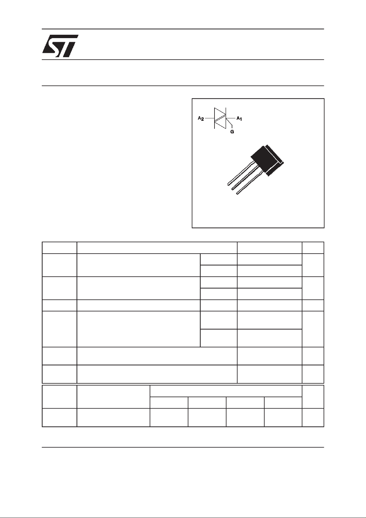
SENSITIVEGATE TRIACS
A
1
A
2
G
TL
(Plastic)
ABSOLUTERATINGS (limitingvalues)
Symbol Parameter Value Unit
I
T(RMS)
I
TSM
I2tI
dI/dt Critical rate of rise of on-state current
Tstg
Tj
Tl Maximum lead temperature for soldering during 4 s at 4.5 mm
Symbol Parameter TLC Unit
RMS on-state current
(360°conduction angle)
Non repetitive surge peak on-state current
( Tj initial= 25°C)
2
t value tp = 10 ms 4.5 A2s
Gate supply : IG= 50mA diG/dt = 0.1A/µs
Storage and operating junction temperature range - 40 to + 150
from case
116 T/D/S/A 226 T/D/S/A 336 T/D/S/A 386 T/D/S/A
Tl= 40°C3 A
Ta = 25°C 1.3 (1)
tp = 8.3 ms 31.5 A
tp = 10 ms 30
Repetitive
F = 50 Hz
Non
Repetitive
10 A/µs
50
- 40 to + 110
230
°C
°
°
C
C
V
DRM
V
RRM
(1) With Cu surface 1cm2.
Repetitive peak off-state
voltage Tj = 110°C
February 1999 Ed: 1A
200 400 600 700 V
1/5
Page 2
TLC 116 T/D/S/ A ---> TLC386 T/ D /S / A
THERMAL RESISTANCES
Symbol Parameter Value Unit
Rth (j-a) Junction to ambient on printed circuit with Cu surface 1cm
Rth (j-l) DC Junction leads for DC 20 °C/W
Rth (j-l) AC Junction leads for 360° conduction angle ( F= 50 Hz) 15 °C/W
2
50 °C/W
GATECHARACTERISTICS (maximumvalues)
P
= 0.1W PGM=2W(tp=20µs) IGM=1A(tp=20µs) VGM= 16V (tp = 20 µs).
G (AV)
ELECTRICAL CHARACTERISTICS
Symbol Test Conditions Quadrant Suffix Unit
TDSA
IGTVD=12V (DC) RL=33Ω Tj=25°C I-II-III MAX 5 5 10 10 mA
IV MAX 5 10 10 25
V
GT
V
GD
tgt VD=V
I
L
VD=12V (DC) RL=33Ω Tj=25°C I-II-III-IV MAX 1.5 V
VD=V
DRMRL
DRMIG
dIG/dt = 0.5A/µs
IG= 1.2 I
=3.3kΩ Tj=110°C I-II-III-IV MIN 0.2 V
= 40mA
GT
Tj=25°C I-II-III-IV TYP 2 µs
Tj=25°C I-III-IV MAX 15 15 25 25 mA
II 15 15 25 25
IH*I
VTM*ITM= 4A tp= 380µs Tj=25°C MAX 1.85 V
I
DRM
I
RRM
dV/dt * Linear slope up to
(dV/dt)c * (dI/dt)c = 1.3A/ms Tj=110°C TYP1155V/µs
* For either polarity of electrodeA2voltage with reference to electrode A1.
2/5
= 100mA gate open Tj=25°C MAX 15 15 25 25 mA
T
V
V
VD=67%V
gate open
DRM
RRM
Rated
Rated
DRM
Tj=25°C MAX 0.01 mA
Tj=110°C MAX 0.75
Tj=110°C TYP 10 10 20 20 V/µs
Page 3

ORDERINGINFORMATION
TLC 11 6 T/D/ S /A ---> TLC386 T / D/S/A
Package I
TLC ..6 3 200 X X X X
Fig.1 : Maximum RMS power dissipation versus RMS
on-state current (F=50Hz).
(Curves are cut off by (dI/dt)c limitation)
T(RMS)
AVTDSA
V
DRM/VRRM
400 XXXX
600 XXXX
700 XXXX
Fig.2 : Correlation between maximum RMS power
dissipation and maximum allowable temperatures (T
and T
lead
Sensitivity Specification
).
amb
Fig.3 : RMS on-state current versus case temperature. Fig.4 : Thermal transient impedance junction to case
and junction to ambient versus pulse duration.
3/5
Page 4

TLC 116 T/D/S/ A ---> TLC386 T/ D /S / A
Fig.5 : Relative variation of gate trigger current and
holding current versus junction temperature.
Fig.6 : Non Repetitive surge peak on-state current
versus number of cycles.
Fig.7 : Non repetitive surge peak on-state current for a
sinusoidal pulse with width : t
corresponding value of I2t.
≤
10ms, and
Fig.8 : On-state characteristics (maximum values).
4/5
Page 5

PACKAGEMECHANICAL DATA
TL Plastic
D
E
F
Marking : type number
Weight : 0.75 g
B
C
TLC 11 6 T/D/ S /A ---> TLC386 T / D/S/A
REF. DIMENSIONS
A
A 9.55 10.05 0.375 0.396
B 7.55 8.05 0.297 0.317
C 12.70 0.500
D 4.25 4.75 0.167 0.187
G
E 1.25 1.75 0.049 0.069
F 6.75 7.25 0.266 0.285
I
G 4.50 0.177
H 2.04 3.04 0.80 0.120
HH
I 0.75 0.85 0.029 0.033
Millimeters Inches
Min. Max. Min. Max.
Information furnished is believed to be accurate and reliable. However, STMicroelectronics assumes no responsibility for the consequences of use of such information nor for any infringement of patents or other rights of third parties which may result from its use. No
license is granted by implication or otherwise under any patent or patent rights of STMicroelectronics. Specifications mentioned in this
publication are subject to change without notice. This publication supersedes and replaces all information previously supplied.
STMicroelectronics products are not authorized for use as critical components in life support devices or systems without express written
approval of STMicroelectronics.
The ST logo is a registered trademark of STMicroelectronics
1999 STMicroelectronics - Printed in Italy - All rights reserved.
STMicroelectronics GROUP OF COMPANIES
Australia - Brazil - Canada - China - France - Germany - Italy - Japan - Korea - Malaysia - Malta - Mexico - Mo-
rocco - The Netherlands - Singapore - Spain - Sweden - Switzerland - Taiwan - Thailand - United Kingdom - U.S.A.
http://www.st.com
5/5
 Loading...