

Page 1
TL431, A, B Series,
NCV431A, B
Programmable
Precision References
The TL431, A, B integrated circuits are three- terminal
programmable shunt regulator diodes. These monolithic IC voltage
references operate as a low temperature coefficient zener which is
programmable from V
devices exhibit a wide operating current range of 1.0mA to 100 mA
with a typical dynamic impedance of 0.22 W. The characteristics of
these references make them excellent replacements for zener diodes in
many applications such as digital voltmeters, power supplies, and op
amp circuitry. The 2.5 V reference makes it convenient to obtain a
stable reference from 5.0 V logic supplies, and since the TL431, A, B
operates as a shunt regulator, it can be used as either a positive or
negative voltage reference.
Features
•Programmable Output Voltage to 36 V
•Voltage Reference Tolerance: ±0.4%, Typ @ 25°C (TL431B)
•Low Dynamic Output Impedance, 0.22 W Typical
•Sink Current Capability of 1.0 mA to 100 mA
•Equivalent Full- Range Temperature Coefficient of 50 ppm/°C Typical
•Temperature Compensated for Operation over Full Rated Operating
Temperature Range
•Low Output Noise Voltage
•Pb-Free Packages are Available
to 36 V with two external resistors. These
ref
http://onsemi.com
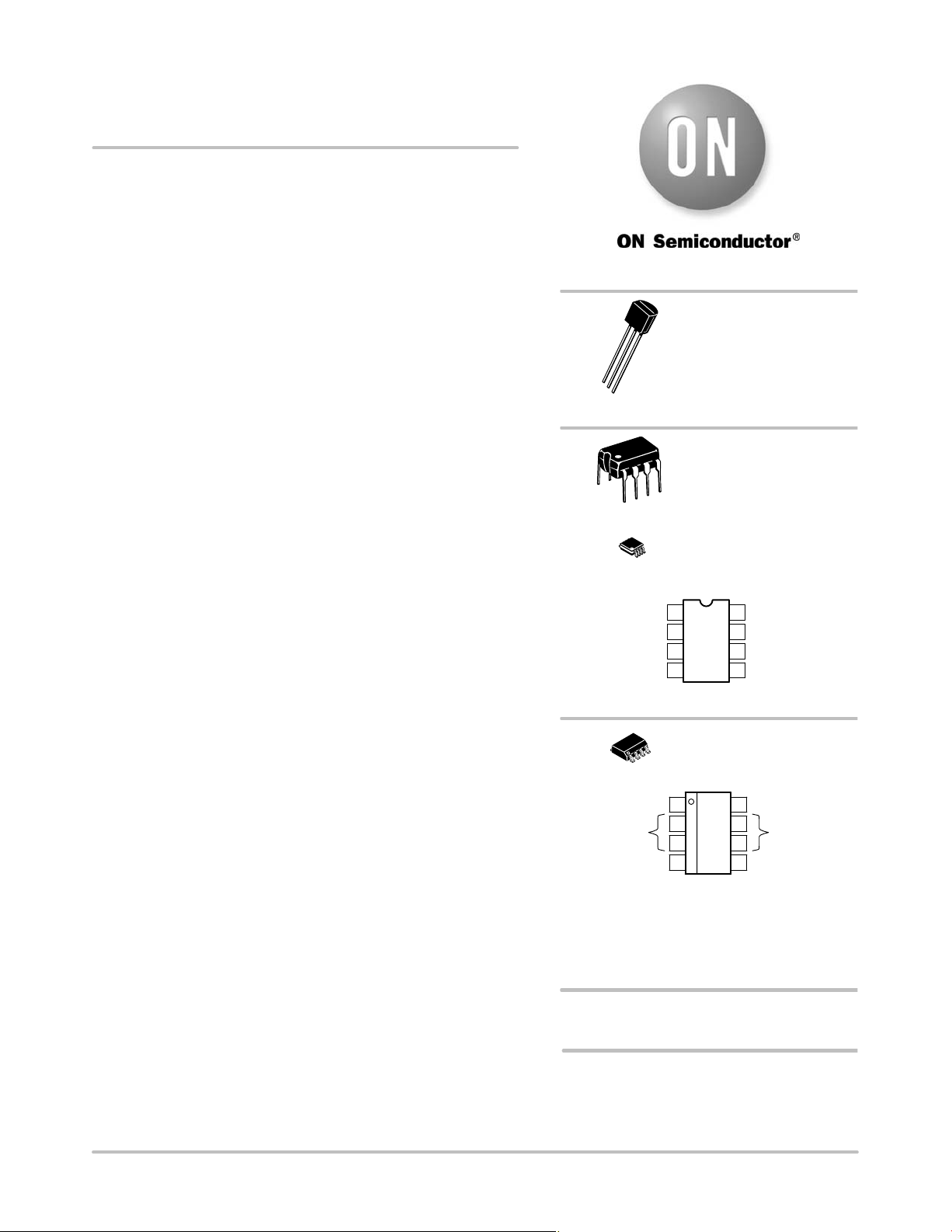
TO-92 (TO-226)
LP SUFFIX
CASE 29
2
3
1
8
Cathode
Pin 1. Reference
2. Anode
3. Cathode
1
1
2
N/C
3
N/C
4
N/C
(Top View)
PDIP-8
P SUFFIX
CASE 626
Micro8E
DM SUFFIX
CASE 846A
8
Reference
7
N/C
6
Anode
5
N/C
1
8
© Semiconductor Components Industries, LLC, 2007
June, 2007 - Rev. 27
SOIC-8
8
1
1
Cathode
N/C
2
3
4
(Top View)
Anode Anode
This is an internally modified SOIC-8 package. Pins 2, 3, 6 and
7 are electrically common to the die attach flag. This internal
lead frame modification increases power dissipation capability
when appropriately mounted on a printed circuit board. This
modified package conforms to all external dimensions of the
standard SOIC-8 package.
D SUFFIX
CASE 751
8
Reference
7
6
5
N/C
ORDERING INFORMATION
See detailed ordering and shipping information in the package
dimensions section on page 13 of this data sheet.
DEVICE MARKING INFORMATION
See general marking information in the device marking
section on page 16 of this data sheet.
1 Publication Order Number:
TL431/D
Page 2
TL431, A, B Series, NCV431A, B
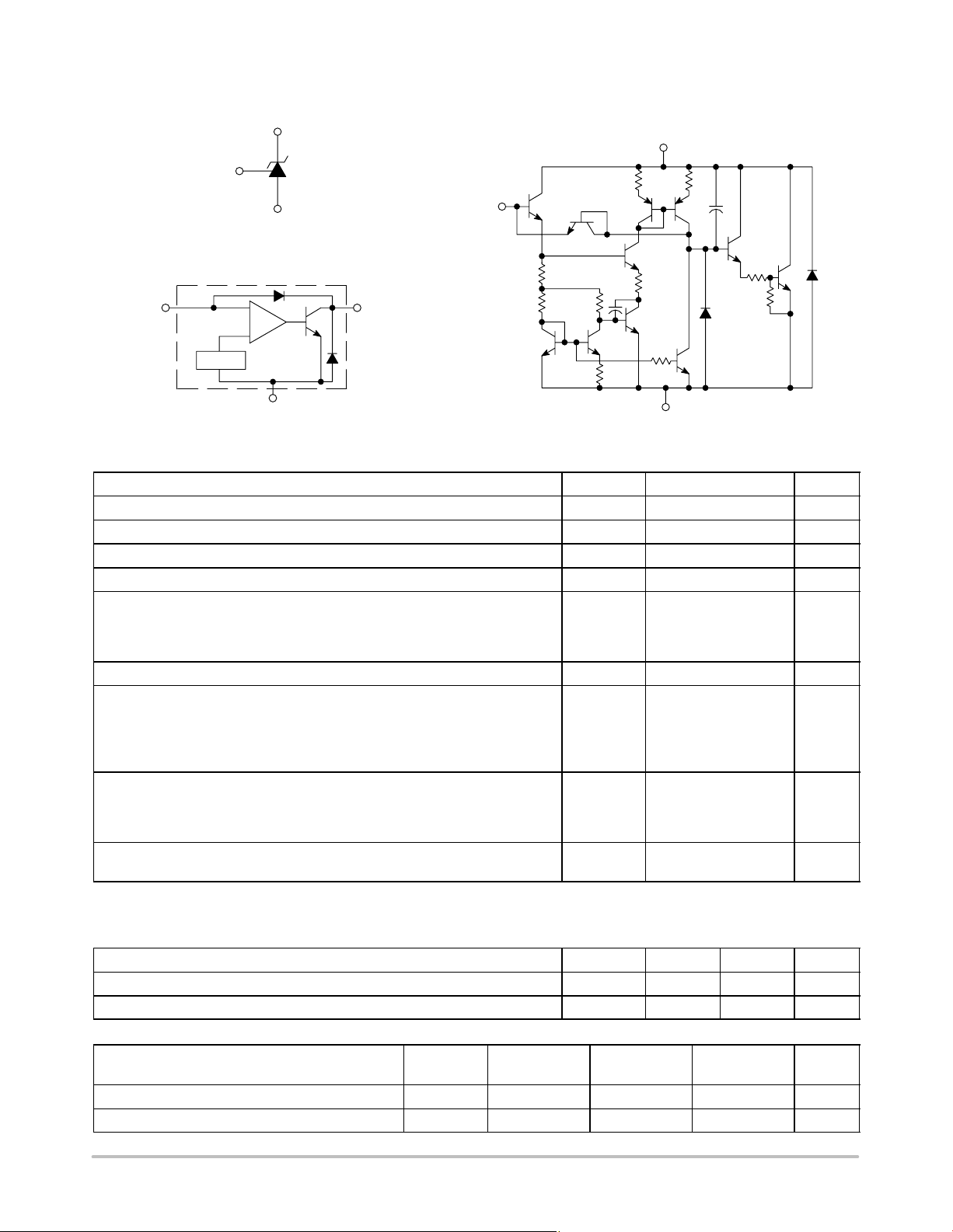
Symbol
Representative Schematic Diagram
Component values are nominal
Cathode
Reference
(R)
Representative Block Diagram
Reference
(R)
2.5 V
+
-
ref
(K)
Anode
(A)
Anode (A)
Cathode
(K)
Reference
(R)
3.28 k
2.4 k 7.2 k
20 pF
800
800
Cathode (K)
800
20 pF
150
4.0 k
10 k
1.0 k
Anode (A)
This device contains 12 active transistors.
MAXIMUM RATINGS (Full operating ambient temperature range applies, unless otherwise noted.)
Rating
Cathode to Anode Voltage V
Cathode Current Range, Continuous I
Reference Input Current Range, Continuous I
Operating Junction Temperature T
Operating Ambient Temperature Range
TL431I, TL431AI, TL431BI -40 to +85
TL431C, TL431AC, TL431BC 0 to +70
NCV431AI, NCV431B, TL431BV -40 to +125
Storage Temperature Range T
Total Power Dissipation @ TA = 25°C P
Derate above 25°C Ambient Temperature
D, LP Suffix Plastic Package 0.70
P Suffix Plastic Package 1.10
DM Suffix Plastic Package 0.52
Total Power Dissipation @ TC = 25°C P
Derate above 25°C Case Temperature
D, LP Suffix Plastic Package 1.5
P Suffix Plastic Package 3.0
ESD Rating HBM
Stresses exceeding Maximum Ratings may damage the device. Maximum Ratings are stress ratings only. Functional operation above the
Recommended Operating Conditions is not implied. Extended exposure to stresses above the Recommended Operating Conditions may affect
device reliability.
Symbol Value Unit
37 V
-100 to +150 mA
-0.05 to +10 mA
150 °C
°C
-65 to +150 °C
W
W
>2000
V
>200
ref
T
stg
MM
KA
K
J
A
D
D
RECOMMENDED OPERATING CONDITIONS
Condition Symbol Min Max Unit
Cathode to Anode Voltage V
Cathode Current I
KA
K
V
ref
36 V
1.0 100 mA
THERMAL CHARACTERISTICS
Characteristic Symbol
Thermal Resistance, Junction-to-Ambient
Thermal Resistance, Junction-to-Case
D, LP Suffix
Package
R
q
JA
R
q
JC
178 114 240 °C/W
83 41 - °C/W
P Suffix
Package
DM Suffix
Package
Unit
http://onsemi.com
2
Page 3
TL431, A, B Series, NCV431A, B
ELECTRICAL CHARACTERISTICS (T
= 25°C, unless otherwise noted.)
A
Characteristic
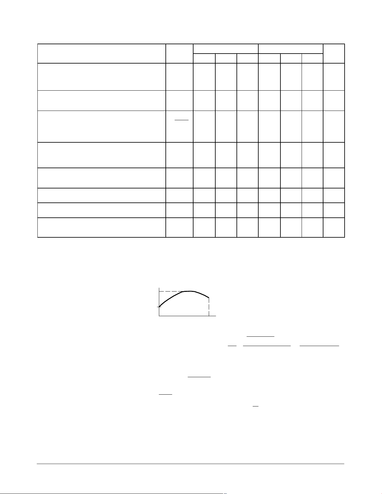
Reference Input Voltage (Figure 1)
V
= V
= 25°C
T
A
TA = T
, IK = 10 mA
ref
to T
low
high
(Note 1)
KA
Reference Input Voltage Deviation Over
Temperature Range (Figure 1, Notes 1, 2)
VKA= V
IK = 10 mA
ref,
Ratio of Change in Reference Input Voltage to Change
in Cathode to Anode Voltage
I
= 10 mA (Figure 2),
K
= 10 V to V
DV
KA
DVKA = 36 V to 10 V
ref
Reference Input Current (Figure 2)
I
= 10 mA, R1 = 10 k, R2 = ∞
K
TA = 25°C
TA = T
low
to T
high
(Note 1)
Reference Input Current Deviation Over
Temperature Range (Figure 2, Note 1, 4)
I
= 10 mA, R1 = 10 k, R2 = ∞
K
Minimum Cathode Current For Regulation
V
= V
KA
(Figure 1)
ref
Off-State Cathode Current (Figure 3)
V
= 36 V, V
KA
ref
= 0 V
Dynamic Impedance (Figure 1, Note 3)
= V
, DIK = 1.0 mA to 100 mA
ref
f ≤ 1.0 kHz
= -40 °C for TL431AIP TL431AILP, TL431IP, TL431ILP, TL431BID, TL431BIP, TL431BILP, TL431AIDM, TL431IDM, TL431BIDM;
=0°C for TL431ACP, TL431ACLP, TL431CP, TL431CLP, TL431CD, TL431ACD, TL431BCD, TL431BCP, TL431BCLP, TL431CDM,
1. T
V
low
KA
TL431ACDM, TL431BCDM
= +85°C for TL431AIP, TL431AILP, TL431IP, TL431ILP, TL431BID, TL431BIP, TL431BILP, TL431IDM, TL431AIDM, TL431BIDM
T
high
= +70°C for TL431ACP, TL431ACLP, TL431CP, TL431ACD, TL431BCD, TL431BCP, TL431BCLP, TL431CDM, TL431ACDM,
TL431BCDM
2. The deviation parameter DV
ambient temperature range that applies.
is defined as the difference between the maximum and minimum values obtained over the full operating
ref
max
V
ref
V
min
ref
TL431I TL431C
Symbol
V
ref
DV
ref
DV
DV
I
ref
DI
ref
I
min
I
off
Min Typ Max Min Typ Max
2.44
2.41
2.495-2.55
2.58
2.44
2.423
- 7.0 30 - 3.0 17 mV
ref
KA
-
-1.4
-
-1.0
-
1.8
-
-2.7
-2.0
4.0
-
6.5
-
-
-
-
- 0.8 2.5 - 0.4 1.2
- 0.5 1.0 - 0.5 1.0 mA
- 20 1000 - 20 1000 nA
2.495-2.55
-1.4
-1.0
1.8
-
|ZKA| - 0.22 0.5 - 0.22 0.5
= V
ref
min
ref
= T2 - T
A
max
ref
1
DV
-V
DT
Unit
V
2.567
mV/V
-2.7
-2.0
mA
4.0
5.2
mA
W
T1
Ambient Temperature
The average temperature coefficient of the reference input voltage, aV
aV
can be positive or negative depending on whether V
ref
Example : DV
+ 8.0mVandslopeispositive,
ref
V
@25_C + 2.495V,DTA+ 70_C
ref
3. The dynamic impedance ZKA is defined as:
ref
|ZKA| +
Min or V
is defined as:
ref
Max occurs at the lower ambient temperature. (Refer to Figure 6.)
ref
0.008x10
aV
+
ref
DV
KA
. When the device is programmed with two external resistors, R1 and R2,
DI
K
(refer to Figure 2) the total dynamic impedance of the circuit is defined as:
http://onsemi.com
70(2.495)
3
T2
ǒ
ppm
V
6
+ 45.8ppmń_C
|ZKAȀ| [ |ZKA|ǒ1 )
ref
_C
+
V
DV
@25_C
ref
R1
R2
Ǔ
ref
DT
6
X10
Ǔ
A
+
DV
DTA(V
x10
ref
@25_C)
ref
6
Page 4
TL431, A, B Series, NCV431A, B
ELECTRICAL CHARACTERISTICS (T
Characteristic
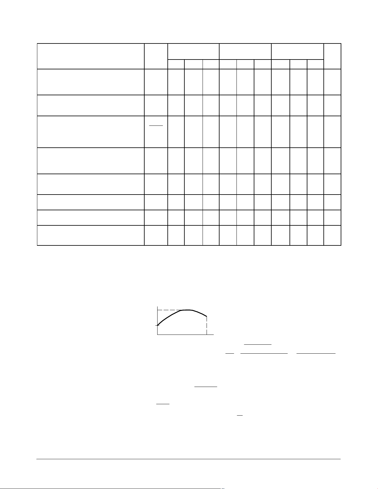
Reference Input Voltage (Figure 1)
V
= V
KA
Reference Input Voltage Deviation Over
Temperature Range (Figure 1, Notes 4, 5)
Ratio of Change in Reference Input Voltage to
Change in Cathode to Anode Voltage
I
K
Reference Input Current (Figure 2)
IK = 10 mA, R1 = 10 k, R2 = ∞
Reference Input Current Deviation Over
Temperature Range (Figure 2, Note 4)
Minimum Cathode Current For Regulation
VKA = V
Off-State Cathode Current (Figure 3)
V
KA
Dynamic Impedance (Figure 1, Note 6)
V
KA
4. T
low
T
high
5. The deviation parameter DV
ambient temperature range that applies.
, IK = 10 mA
ref
TA = 25°C
TA = T
V
KA
= V
to T
low
IK = 10 mA
ref,
high
= 10 mA (Figure 2),
= 10 V to V
DV
KA
DVKA = 36 V to 10V
ref
TA = 25°C
TA = T
low
to T
high
(Note 4)
IK = 10 mA, R1 = 10 k, R2 = ∞
(Figure 1)
ref
= 36 V, V
= V
f ≤ 1.0 kHz
= 0 V
ref
, DIK = 1.0 mA to 100 mA
ref
= -40 °C for TL431AIP TL431AILP, TL431IP, TL431ILP, TL431BID, TL431BIP, TL431BILP, TL431BV, TL431AIDM, TL431IDM,
TL431BIDM, NCV431AIDMR2, NCV431AIDR2
=0°C for TL431ACP, TL431ACLP, TL431CP, TL431CLP, TL431CD, TL431ACD, TL431BCD, TL431BCP, TL431BCLP, TL431CDM,
TL431ACDM, TL431BCDM
= +85°C for TL431AIP, TL431AILP, TL431IP, TL431ILP, TL431BID, TL431BIP, TL431BILP, TL431IDM, TL431AIDM, TL431BIDM
= +70°C for TL431ACP, TL431ACLP, TL431CP, TL431ACD, TL431BCD, TL431BCP, TL431BCLP, TL431CDM, TL431ACDM,
TL431BCDM
= +125°C TL431BV, NCV431AIDMR2, NCV431AIDR2, NCV431BVDMR2G
is defined as the difference between the maximum and minimum values obtained over the full operating
ref
= 25°C, unless otherwise noted.)
A
TL431BI / TL431BV
TL431AI / NCV431AI TL431AC
Symbol
V
DV
DV
DV
I
DI
I
I
Min Typ Max Min Typ Max Min Typ Max
ref
2.47
2.495-2.52
2.44
- 7.0 30 - 3.0 17 - 3.0 17 mV
ref
2.55
2.47
2.453
2.495-2.52
2.537
2.483
2.475
ref
KA
ref
min
off
---1.4
-
-
ref
- 0.8 2.5 - 0.4 1.2 - 0.8 2.5
- 0.5 1.0 - 0.5 1.0 - 0.5 1.0 mA
- 20 1000 - 20 1000 - 0.23 500 nA
-2.7
-1.0
-2.0--
1.8-4.0
6.5--
-1.4
-2.7
-1.0
-2.0
1.8-4.0
5.2
-
-
-
-
|ZKA| - 0.22 0.5 - 0.22 0.5 - 0.14 0.3
max
V
ref
V
min
ref
DV
-V
DT
= V
ref
min
ref
= T2 - T
A
max
ref
1
NCV431BV
2.495
2.495
-1.4
-1.0
1.1-2.0
Unit
V
2.507
2.515
mV/V
-2.7
-2.0
mA
4.0
mA
W
T1
Ambient Temperature
The average temperature coefficient of the reference input voltage, aV
aV
can be positive or negative depending on whether V
ref
Example : DV
+ 8.0mVandslopeispositive,
ref
V
@25_C + 2.495V,DTA+ 70_C
ref
6. The dynamic impedance ZKA is defined as
ref
|ZKA| +
Min or V
ref
DV
KA
When the device is programmed with two external resistors, R1 and R2, (refer
DI
K
to Figure 2) the total dynamic impedance of the circuit is defined as:
7. NCV431AIDMR2, NCV431AIDR2, NCV431BVDMR2G T
and other applications requiring site and change control.
low
http://onsemi.com
T2
is defined as:
ref
Max occurs at the lower ambient temperature. (Refer to Figure 6.)
0.008x10
aV
+
ref
70(2.495)
|ZKAȀ| [ |ZKA|ǒ1 )
= -40°C, T
= +125°C. Guaranteed by design. NCV prefix is for automotive
high
ppm
V
ref
_C
6
+ 45.8ppmń_C
DV
ref
ǒ
V
@25_C
ref
+
R1
R2
DT
A
Ǔ
Ǔ
X10
6
+
4
DV
DTA(V
x10
ref
@25_C)
ref
6
Page 5
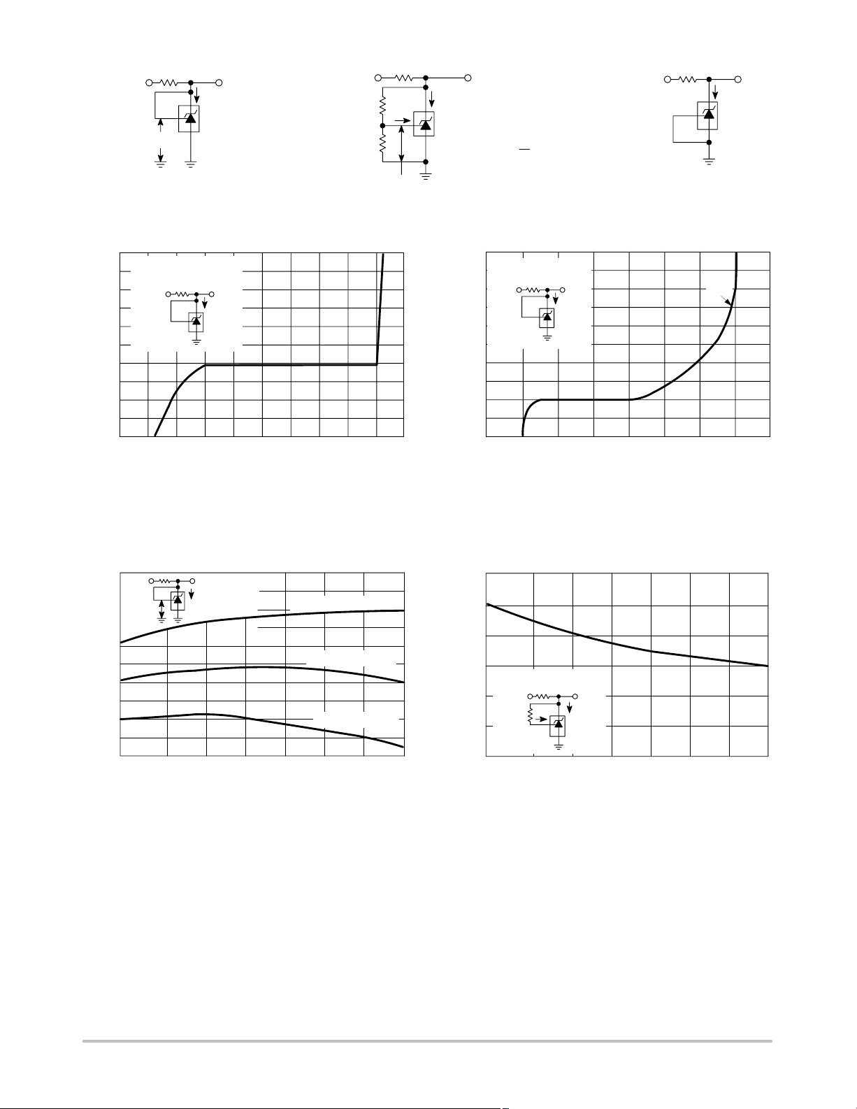
TL431, A, B Series, NCV431A, B
Input
V
ref
V
KA
I
K
Figure 1. Test Circuit for VKA = V
150
VKA = V
ref
100
TA = 25°C
Input V
I
K
KA
50
0
, CATHODE CURRENT (mA)
-50
K
I
-100
-2.0 -1.0 0
, CATHODE VOLTAGE (V)
V
KA
Figure 4. Cathode Current versus
Cathode Voltage
Input
R1
R2
V
ref
ref
Figure 2. Test Circuit for V
1.0 2.0 3.0
V
KA
I
I
K
ref
ref
ǒ1 )
KA
> V
R1
R2
Ǔ) I
ref
SR1
ref
Figure 3. Test Circuit for I
VKA+ V
Input V
I
off
KA
off
800
V
= V
KA
ref
600
Input
TA = 25°C
V
KA
I
K
I
Min
400
200
, CATHODE CURRENT ( A)μ
0
K
I
-200
-1.0
0
V
, CATHODE VOLTAGE (V)
KA
1.0 2.0 3.0
Figure 5. Cathode Current versus
Cathode Voltage
2600
2580
2560
2540
2520
2500
2480
2460
2440
2420
ref
V , REFERENCE INPUT VOLTAGE (mV)
2400
-55
V
Input
V
ref
KA
I
K
VKA = V
ref
IK = 10 mA
050
25-25
T
, AMBIENT TEMPERATURE (°C)
A
V
ref
Max = 2550 mV
V
Typ = 2495 mV
ref
V
Min = 2440 mV
ref
75 100 125
Figure 6. Reference Input Voltage versus
Ambient Temperature
3.0
2.5
2.0
1.5
IK = 10 mA
Input
1.0
0.5
, REFERENCE INPUT CURRENT ( A)μ
ref
I
0
10k
I
ref
V
KA
I
K
250-25
T
, AMBIENT TEMPERATURE (°C)
A
125
10050 75-55
Figure 7. Reference Input Current versus
Ambient Temperature
http://onsemi.com
5
Page 6
TL431, A, B Series, NCV431A, B
0
-8.0
-16
-24
, REFERENCE INPUT VOLTAGE (mV)Δ
ref
V
-32
100
Ω|, DYNAMIC IMPEDANCE ( )
10
Input V
R1
R2
V
ref
KA
I
K
20
VKA, CATHODE VOLTAGE (V)
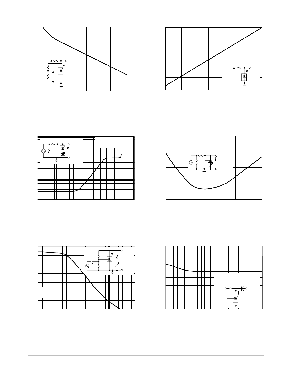
Figure 8. Change in Reference Input
Voltage versus Cathode Voltage
1.0 k
50
Output
I
K
-
+
GND
TA = 25°C
D I
K
IK = 10 mA
T
= 25°C
A
30100
= 1.0 mA to 100 mA
1.0 k
100
10
VKA = 36 V
= 0 V
V
1.0
Input
ref
V
KA
I
off
0.1
, OFF-STATE CATHODE CURRENT (nA)
off
I
0.01
40
-55
T
, AMBIENT TEMPERATURE (5C)
A
75-25 0 25 50 100 125
Figure 9. Off-State Cathode Current
versus Ambient Temperature
0.320
V
= V
KA
Ω|, DYNAMIC IMPEDANCE ( )
0.300
0.280
0.260
ref
D IK = 1.0 mA to 100 mA
f ≤ 1.0 kHz
1.0k
50
Output
I
K
+
GND
1.0
KA
|Z
0.1
60
50
40
30
20
IK = 10 mA
10
, OPEN LOOP VOLTAGE GAIN (dB)
A
TA = 25°C
0
VOL
-10
1.0 k 10 k
100 k 10 M1.0 M1.0 k 10 k
f, FREQUENCY (MHz)
Figure 10. Dynamic Impedance
versus Frequency
I
K
15k
9.0 mF
8.25k
100 k
f, FREQUENCY (MHz)
230
Output
GND
0.240
KA
0.220
|Z
0.200
-55
T
, AMBIENT TEMPERATURE (°C)
A
75-25 0 25 50 100 125
Figure 11. Dynamic Impedance
versus Ambient Temperature
80
60
√
VKA = V
40
20
NOISE VOLTAGE (nV/ Hz)
0
10 M1.0 M
10 10 k1.0 k100
f, FREQUENCY (Hz)
I
= 10 mA
K
T
= 25°C
A
ref
OutputInput
I
K
100 k
Figure 12. Open-Loop Voltage Gain
versus Frequency
Figure 13. Spectral Noise Density
http://onsemi.com
6
Page 7
TL431, A, B Series, NCV431A, B
TA = 25°C
3.0
2.0
1.0
0
VOLTAGE SWING (V)
5.0
0
0 8.04.0 20
Output
Input
t, TIME (ms)
Input
Monitor
Pulse
Generator
f = 100 kHz
12
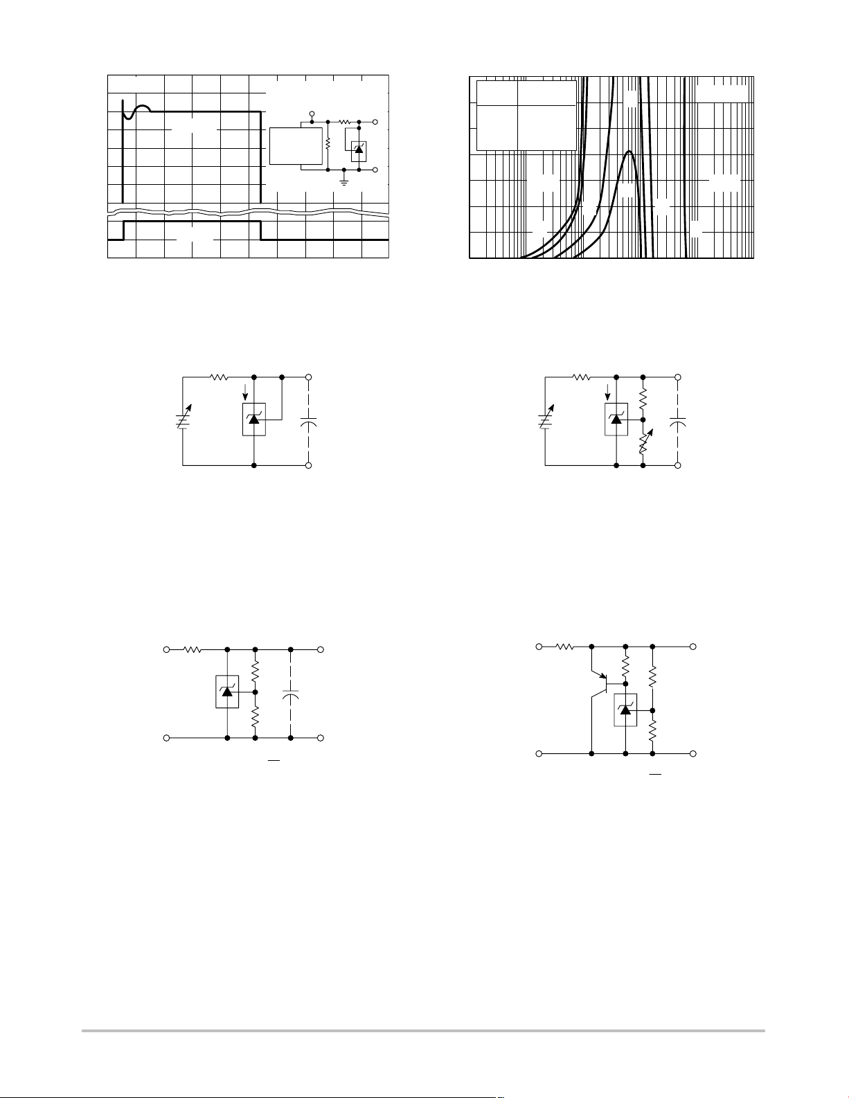
Figure 14. Pulse Response Figure 15. Stability Boundary Conditions
150
I
K
V+
C
140
Unstable
, CATHODE CURRENT (mA)
K
I
120
100
80
60
40
20
0
1.0 nF
Output
220
50
GND
16
L
Programmed
Area
A
B
C
D
(V)
V
KA
V
ref
5.0
10
15
Stable Stable
A
10 nF 100 nF
, LOAD CAPACITANCE
C
L
150
V+
C
D
B
I
K
10 k
TA = 25°C
B
A
100 mF1.0 mF10 mF
C
L
Figure 16. Test Circuit For Curve A
of Stability Boundary Conditions
Figure 17. Test Circuit For Curves B, C, And D
of Stability Boundary Conditions
TYPICAL APPLICATIONS
V+
R1
R2
R1
ǒ
V
+
out
1 )
R2
Ǔ
V
V
out
ref
Figure 18. Shunt Regulator Figure 19. High Current Shunt Regulator
V+ V
R1
R2
R1
ǒ
Ǔ
1 )
V
+
out
R2
V
out
ref
http://onsemi.com
7
Page 8
TL431, A, B Series, NCV431A, B
MC7805
V+ V
In
V
Common
V
out
out(min)
+
Out
ǒ
1 )
+ V
R1
R2
ref
Ǔ
V
ref
) 5.0V
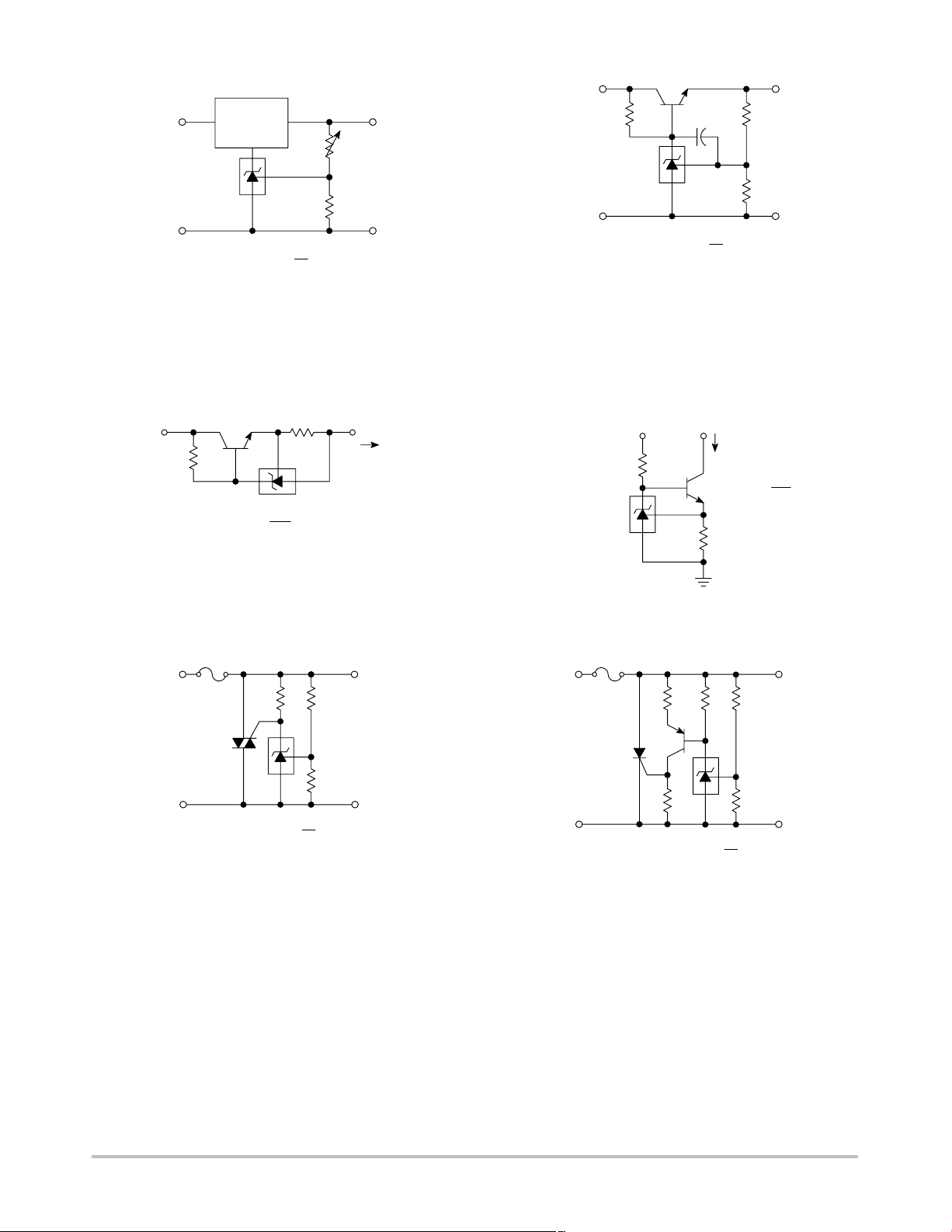
Figure 20. Output Control for a
Three-T erminal Fixed Regulator
R
V+
I
+
out
CL
V
ref
R
CL
R2
R1
V+
out
R1
ǒ
Ǔ
1 )
out
+ V
R2
) V
ref
V
ref
be
V
out
V
in(min)
+
V
out(min)
+ V
R1
R2
V
out
Figure 21. Series Pass Regulator
I
out
V+
I
sink
V
I
Sink
R
S
ref
+
R
S
Figure 22. Constant Current Source Figure 23. Constant Current Sink
V+
V
out(trip)
+
ǒ
1 )
R1
R2
V
out
R1
R2
Ǔ
V
ref
V+
V
out(trip)
+
ǒ
1 )
R1
R2
R1
R2
Ǔ
V
ref
Figure 24. TRIAC Crowbar Figure 25. SRC Crowbar
V
out
http://onsemi.com
8
Page 9
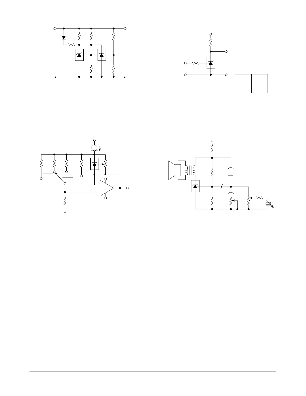
TL431, A, B Series, NCV431A, B
5.0 k
1%
10 kW
1.0 kW
V
V+
l
L.E.D. indicator is `on' when V+ is between the
upper and lower limits.
LowerLimit +
UpperLimit +
R1 R3
R2 R4
R1
ǒ
1 )
R2
R3
ǒ
1 )
R4
Figure 26. Voltage Monitor Figure 27. Single-Supply Comparator with
25 V
V
W
D
Range
out
V
50 k
1%
1N5305
5.0 M
500 k
V
R
1%
X
100 kW
V
Range
1%
1.0 MW
Rx+ V
Ǔ
V
Ǔ
V
2.0 mA
-
LM11
+
ref
ref
Calibrate
25 V
-5.0 V
10 k
V
out
V
in
Vth = V
V+
V
out
ref
V
< V
> V
V
in
out
V+
ref
≈ 2.0 V
ref
Temperature-Compensated Threshold
38 V
T
= 330 to 8.0 W
l
T
I
8.0 W
V
out
*Thermalloy
*THM 6024
*Heatsink on
*LP Package
*
330
+
470 mF
360 k
1.0 mF
0.05 mF
Tone
56 k 10 k 25 k
Volume
47 k
Figure 28. Linear Ohmmeter Figure 29. Simple 400 mW Phono Amplifier
http://onsemi.com
9
Page 10
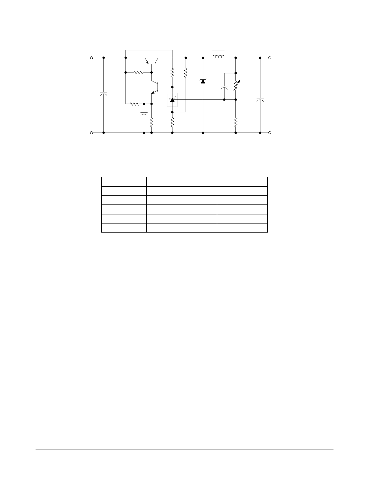
TL431, A, B Series, NCV431A, B
= 10 V to 20 V
V
in
150 mH @ 2.0 A
TIP115
1.0 k
4.7 k
+
2200 mF
MPSA20
4.7 k
0.1 mF
102.2 k
4.7 k
1N5823
0.01mF
100 k
51 k
Figure 30. High Efficiency Step-Down Switching Converter
Test Conditions Results
Line Regulation Vin = 10 V to 20 V, Io = 1.0 A 53 mV (1.1%)
Load Regulation Vin = 15 V, Io = 0 A to 1.0 A 25 mV (0.5%)
Output Ripple Vin = 10 V, Io = 1.0 A 50 mVpp P.A.R.D.
Output Ripple Vin = 20 V, Io = 1.0 A 100 mVpp P.A.R.D.
Efficiency Vin = 15 V, Io = 1.0 A 82%
470 mF
= 5.0 V
V
out
I
= 1.0 A
out
+
http://onsemi.com
10
Page 11

TL431, A, B Series, NCV431A, B
APPLICATIONS INFORMATION
The TL431 is a programmable precision reference which
is used in a variety of ways. It serves as a reference voltage
in circuits where a non-standard reference voltage is
needed. Other uses include feedback control for driving an
optocoupler in power supplies, voltage monitor, constant
current source, constant current sink and series pass
regulator. In each of these applications, it is critical to
maintain stability of the device at various operating currents
and load capacitances. In some cases the circuit designer can
estimate the stabilization capacitance from the stability
boundary conditions curve provided in Figure 15. However,
these typical curves only provide stability information at
specific cathode voltages and at a specific load condition.
Additional information is needed to determine the
capacitance needed to optimize phase margin or allow for
process variation.
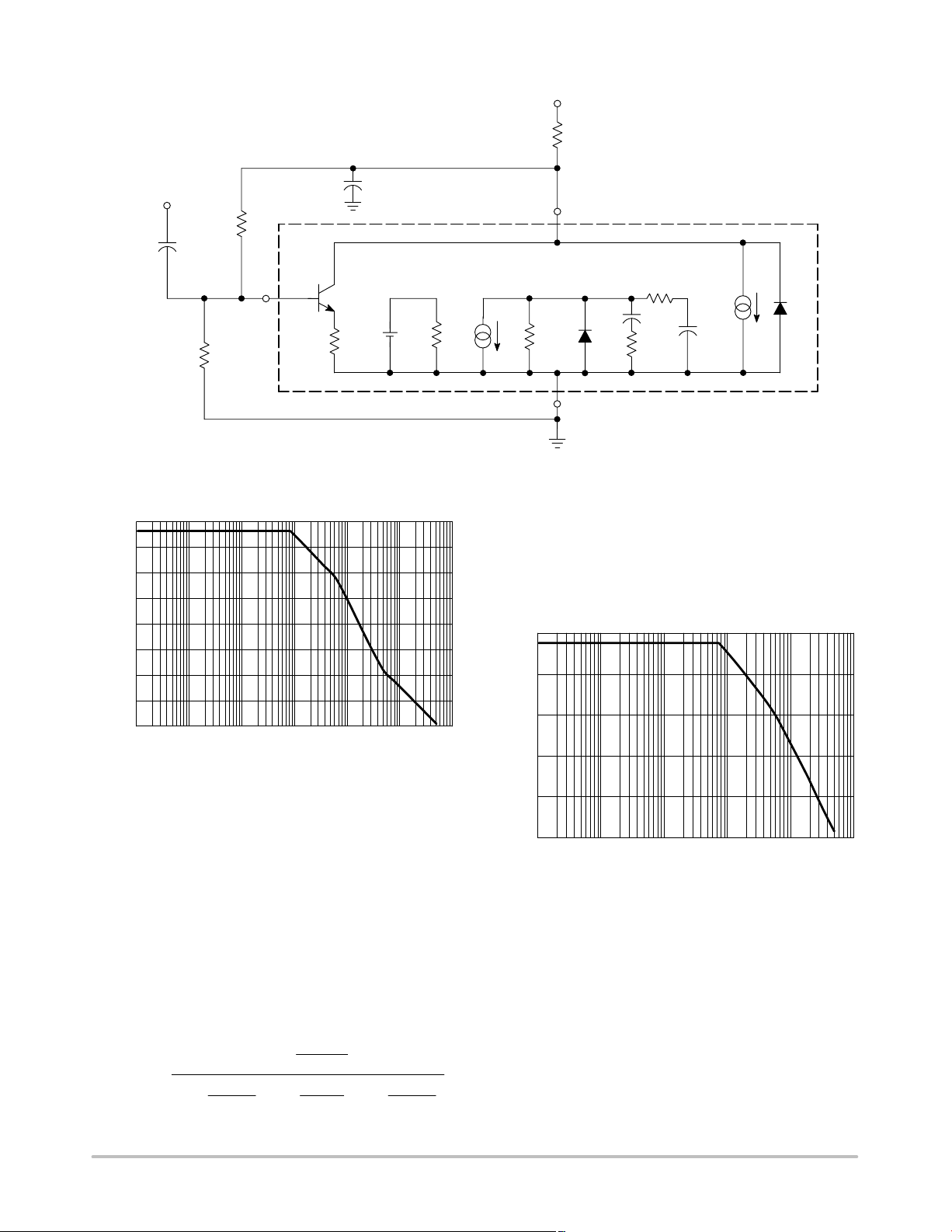
A simplified model of the TL431 is shown in Figure 31.
When tested for stability boundaries, the load resistance is
150 W. The model reference input consists of an input
transistor and a dc emitter resistance connected to the device
anode. A dependent current source, Gm, develops a current
whose amplitude is determined by the difference between
the 1.78 V internal reference voltage source and the input
transistor emitter voltage. A portion of Gm flows through
compensation capacitance, C
. The voltage across C
P2
P2
drives the output dependent current source, Go, which is
connected across the device cathode and anode.
Model component values are:
V
= 1.78 V
ref
Gm = 0.3 + 2.7 exp (-I
where IC is the device cathode current and Gm is in mhos
/26 mA)
C
Go = 1.25 (Vcp2) mmhos.
Resistor and capacitor typical values are shown on the
model. Process tolerances are ±20% for resistors, ±10% for
capacitors, and ±40% for transconductances.
An examination of the device model reveals the location
of circuit poles and zeroes:
P1 +
1
2pRGMC
+
2p * 1.0M * 20pF
P1
1
+ 7.96kHz
P2 +
Z1 +
1
2pRP2C
1
2pRZ1C
+
2p * 10M * 0.265pF
P2
+
2p * 15.9k * 20pF
P1
1
1
+ 60kHz
+ 500kHz
In addition, there is an external circuit pole defined by the
load:
PL+
1
2pRLC
L
Also, the transfer dc voltage gain of the TL431 is:
G + GMRGMGoR
L
Example 1:
IC+10mA, RL+ 230W,CL+ 0.Definethetransfergain.
The DC gain is:
G + GMRGMGoRL+
(2.138)(1.0M)(1.25m)(230) + 615 + 56dB
Loopgain + G
8.25k
8.25k ) 15k
+ 218 + 47dB
The resulting transfer function Bode plot is shown in
Figure 32. The asymptotic plot may be expressed as the
following equation:
Av + 615
ǒ
1 )
ǒ
1 )
8.0kHz
jf
jf
500kHz
Ǔǒ
1 )
Ǔ
jf
60kHz
Ǔ
The Bode plot shows a unity gain crossover frequency of
approximately 600 kHz. The phase margin, calculated from
the equation, would be 55.9 degrees. This model matches the
Open-Loop Bode Plot of Figure 12. The total loop would
have a unity gain frequency of about 300 kHz with a phase
margin of about 44 degrees.
http://onsemi.com
11
Page 12
Input
8.25 k
9.0 mF
15 k
TL431, A, B Series, NCV431A, B
V
CC
R
L
C
L
3
Cathode
R
P2
Ref
1
500 k
V
ref
1.78 V
G
+
R
ref
-
16
M
R
GM
1.0 M
Anode 2
20 pF
10 M
C
P1
R
Z1
15.9 k
Figure 31. Simplified TL431 Device Model
Go
1.0 mmho
C
P2
0.265 pF
TL431 OPEN-LOOP VOLTAGE GAIN VERSUS FREQUENCY
60
50
40
30
20
10
0
-10
Av, OPEN-LOOP VOLTAGE GAIN (dB)
-20
10
2
1
10
3
10
f, FREQUENCY (Hz)
4
10
5
10
6
10
10
Figure 32. Example 1 Circuit Open Loop Gain Plot
Example 2.
= 7.5 mA, RL = 2.2 kW, CL = 0.01 mF. Cathode tied to
I
C
reference input pin. An examination of the data sheet
stability boundary curve (Figure 15) shows that this value of
load capacitance and cathode current is on the boundary.
Define the transfer gain.
The DC gain is:
G + GMRGMGoRL+
(2.323)(1.0M)(1.25m)(2200) + 6389 + 76dB
The resulting open loop Bode plot is shown in Figure 33.
The asymptotic plot may be expressed as the following
equation:
1 )
jf
500kHz
jf
60kHz
Ǔ
Ǔǒ
1 )
jf
7.2kHz
Ǔ
Av + 615
ǒ
1 )
jf
8.0kHz
Ǔǒ
ǒ
1 )
Note that the transfer function now has an extra pole
formed by the load capacitance and load resistance.
Note that the crossover frequency in this case is about
250 kHz, having a phase margin of about -46 degrees.
Therefore, instability of this circuit is likely.
80
60
40
7
20
Av, OPEN-LOOP GAIN (dB)
0
-20
Figure 33. Example 2 Circuit Open Loop Gain Plot
TL431 OPEN-LOOP BODE PLOT WITH LOAD CAP
1
10
2
10
3
10
f, FREQUENCY (Hz)
10
4
With three poles, this system is unstable. The only hope
for stabilizing this circuit is to add a zero. However, that can
only be done by adding a series resistance to the output
capacitance, which will reduce its effectiveness as a noise
filter. Therefore, practically, in reference voltage
applications, the best solution appears to be to use a smaller
value of capacitance in low noise applications or a very
large value to provide noise filtering and a dominant pole
rolloff of the system.
5
10
6
10
http://onsemi.com
12
Page 13
TL431, A, B Series, NCV431A, B
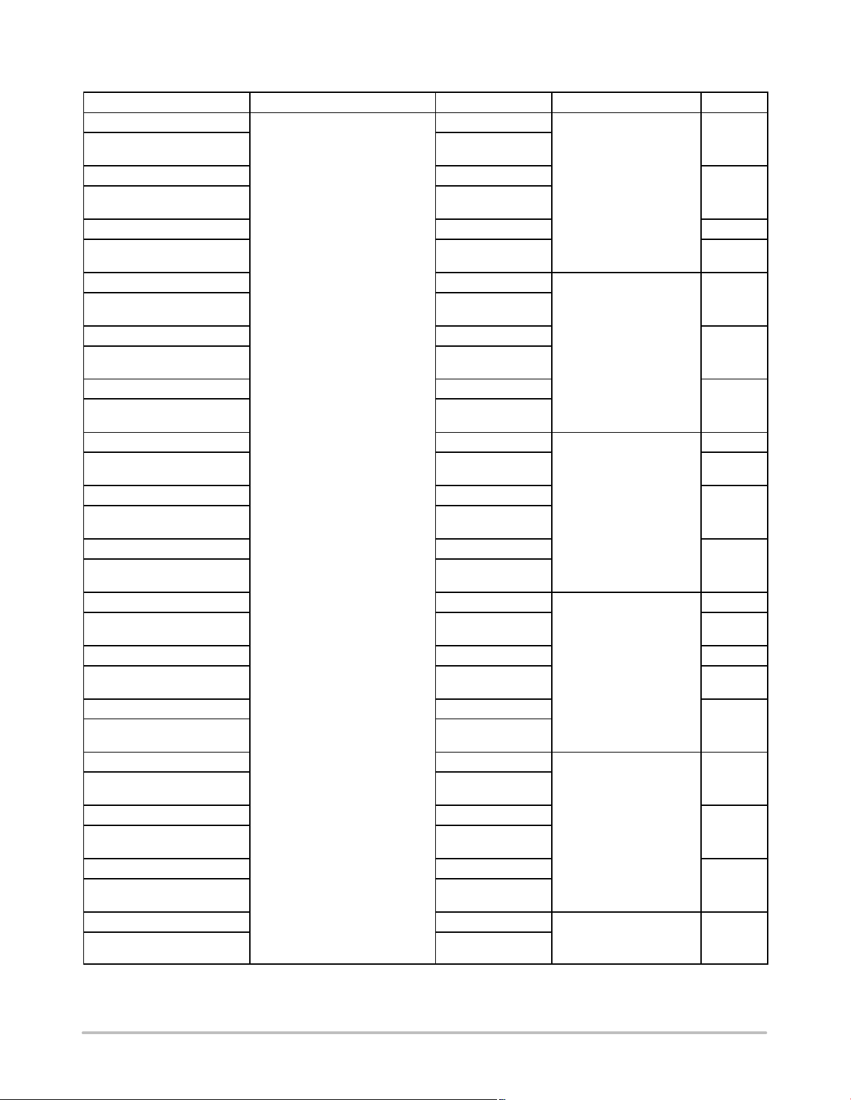
ORDERING INFORMATION
Device Operating Temperature Range Package Code Shipping Information
TL431ACD
TL431ACDG
TL431BCD
TL431BCDG
TL431CD
TL431CDG
TL431ACDR2
TL431ACDR2G
TL431BCDR2
TL431BCDR2G
TL431CDR2
TL431CDR2G
TL431ACDMR2
TL431ACDMR2G
TL431BCDMR2
TL431BCDMR2G
TL431CDMR2
TL431CDMR2G
TL431ACP
TL431ACPG
TL431BCP
TL431BCPG
TL431CP
TL431CPG
TL431ACLP
TL431ACLPG
TL431BCLP
TL431BCLPG
TL431CLP
TL431CLPG
TL431ACLPRA
TL431ACLPRAG
†For information on tape and reel specifications, including part orientation and tape sizes, please refer to our Tape and Reel Packaging
Specifications Brochure, BRD8011/D.
0°C to 70°C
SOIC-8
SOIC-8
(Pb-Free)
SOIC-8
SOIC-8
(Pb-Free)
SOIC-8 2.2%
SOIC-8
(Pb-Free)
SOIC-8
SOIC-8
(Pb-Free)
SOIC-8
SOIC-8
(Pb-Free)
SOIC-8
SOIC-8
(Pb-Free)
Micro8
Micro8
(Pb-Free)
Micro8
Micro8
(Pb-Free)
Micro8
Micro8
(Pb-Free)
PDIP-8
PDIP-8
(Pb-Free)
PDIP-8 0.4%
PDIP-8
(Pb-Free)
PDIP-8
PDIP-8
(Pb-Free)
TO-92 (TO-226)
TO-92 (TO-226)
(Pb-Free)
TO-92 (TO-226)
TO-92 (TO-226)
(Pb-Free)
TO-92 (TO-226)
TO-92 (TO-226)
(Pb-Free)
TO-92 (TO-226)
TO-92 (TO-226)
(Pb-Free)
98 Units / Rail
2500 Units / Tape & Reel
4000 Units / Tape & Reel
50 Units / Rail
2000 Units / Bag
2000 Units / Tape & Reel 1.0%
†
Tolerance
1.0%
0.4%
2.2%
1.0%
0.4%
2.2%
1.0%
1.0%
0.4%
2.2%
1.0%
1.0%
0.4%
2.2%
1.0%
0.4%
2.2%
http://onsemi.com
13
Page 14
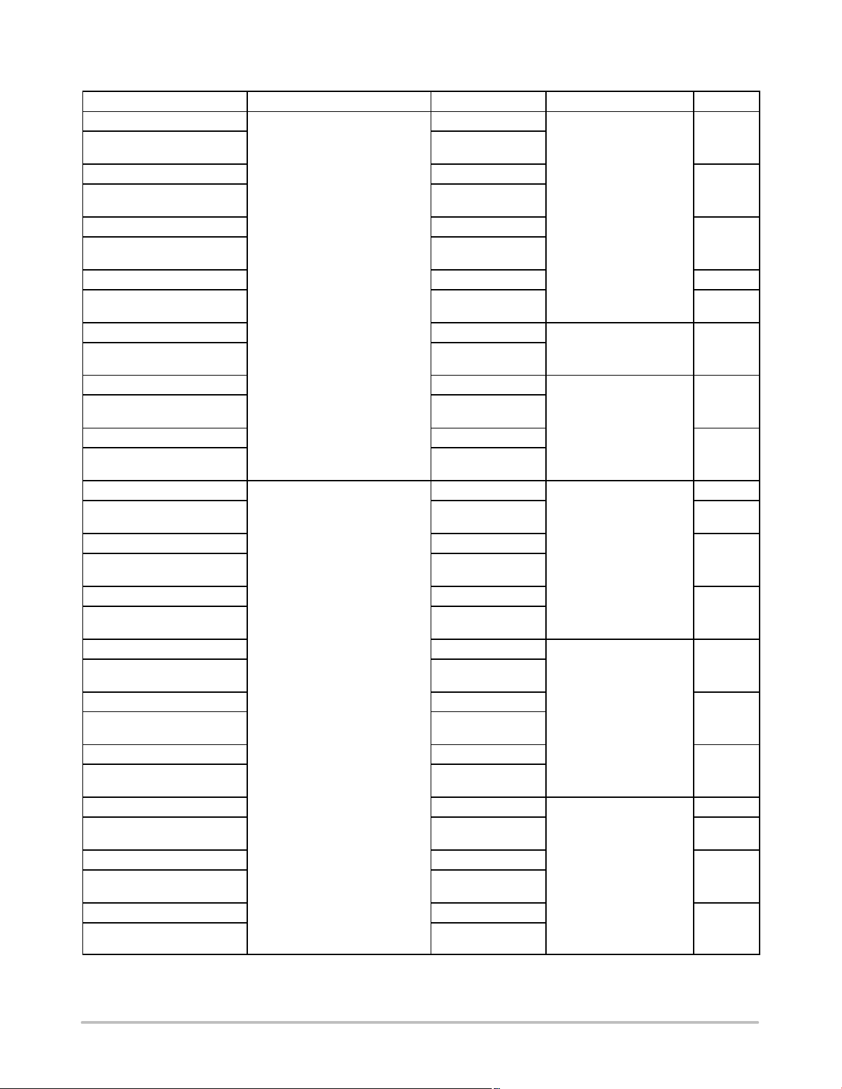
TL431, A, B Series, NCV431A, B
ORDERING INFORMATION
Device Operating Temperature Range Package Code Shipping Information
TL431BCLPRA
TL431BCLPRAG
TL431CLPRA
TL431CLPRAG
TL431ACLPRE
TL431ACLPREG
TL431BCLPRE
TL431BCLPREG
TL431ACLPRP
TL431ACLPRPG
TL431BCLPRM
TL431BCLPRMG
TL431CLPRP
TL431CLPRPG
TL431AID
TL431AIDG
TL431BID
TL431BIDG
TL431ID
TL431IDG
TL431AIDR2
TL431AIDR2G
TL431BIDR2
TL431BIDR2G
TL431IDR2
TL431IDR2G
TL431AIDMR2
TL431AIDMR2G
TL431BIDMR2
TL431BIDMR2G
TL431IDMR2
TL431IDMR2G
†For information on tape and reel specifications, including part orientation and tape sizes, please refer to our Tape and Reel Packaging
Specifications Brochure, BRD8011/D.
0°C to 70°C
-40 °C to 85°C
TO-92 (TO-226)
TO-92 (TO-226)
(Pb-Free)
TO-92 (TO-226)
TO-92 (TO-226)
(Pb-Free)
TO-92 (TO-226)
TO-92 (TO-226)
(Pb-Free)
TO-92 (TO-226) 0.4%
TO-92 (TO-226)
(Pb-Free)
TO-92 (TO-226)
TO-92 (TO-226)
(Pb-Free)
TO-92 (TO-226)
TO-92 (TO-226)
(Pb-Free)
TO-92 (TO-226)
TO-92 (TO-226)
(Pb-Free)
SOIC-8
SOIC-8
(Pb-Free)
SOIC-8
SOIC-8
(Pb-Free)
SOIC-8
SOIC-8
(Pb-Free)
SOIC-8
SOIC-8
(Pb-Free)
SOIC-8
SOIC-8
(Pb-Free)
SOIC-8
SOIC-8
(Pb-Free)
Micro8
Micro8
(Pb-Free)
Micro8
Micro8
(Pb-Free)
Micro8
Micro8
(Pb-Free)
2000 Units / Tape & Reel
2000 / Tape & Ammo Box 1.0%
2000 Units / Fan-Fold
98 Units / Rail
2500 Units / Tape & Reel
4000 Units / Tape & Reel
†
Tolerance
0.4%
2.2%
1.0%
0.4%
0.4%
2.2%
1.0%
1.0%
0.4%
2.2%
1.0%
0.4%
2.2%
1.0%
1.0%
0.4%
2.2%
http://onsemi.com
14
Page 15
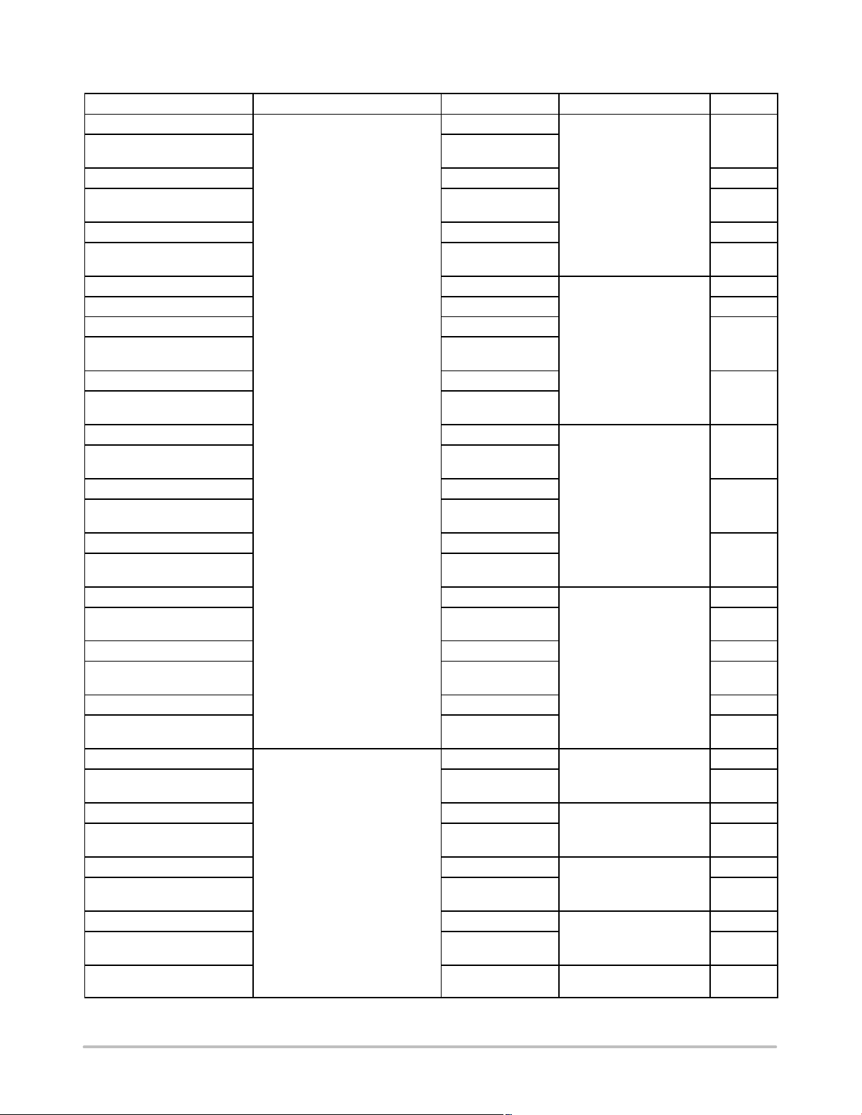
TL431, A, B Series, NCV431A, B
ORDERING INFORMATION
Device Operating Temperature Range Package Code Shipping Information
TL431AIP
TL431AIPG
TL431BIP
TL431BIPG
TL431IP
TL431IPG
TL431AILP
TL431AILPG
TL431BILP
TL431BILPG
TL431ILP
TL431ILPG
TL431AILPRA
TL431AILPRAG
TL431BILPRA
TL431BILPRAG
TL431ILPRA
TL431ILPRAG
TL431AILPRM
TL431AILPRMG
TL431AILPRP
TL431AILPRPG
TL431ILPRP
TL431ILPRPG
TL431BVD
TL431BVDG
TL431BVDR2
TL431BVDR2G
TL431BVDMR2
TL431BVDMR2G
TL431BVLP
TL431BVLPG
TL431BVLPRAG
†For information on tape and reel specifications, including part orientation and tape sizes, please refer to our Tape and Reel Packaging
Specifications Brochure, BRD8011/D.
-40 °C to 85°C
-40 °C to 125°C
PDIP-8
PDIP-8
(Pb-Free)
PDIP-8 0.4%
PDIP-8
(Pb-Free)
PDIP-8 2.2%
PDIP-8
(Pb-Free)
TO-92 (TO-226)
TO-92 (TO-226) 1.0%
TO-92 (TO-226)
TO-92 (TO-226)
(Pb-Free)
TO-92 (TO-226)
TO-92 (TO-226)
(Pb-Free)
TO-92 (TO-226)
TO-92 (TO-226)
(Pb-Free)
TO-92 (TO-226)
TO-92 (TO-226)
(Pb-Free)
TO-92 (TO-226)
TO-92 (TO-226)
(Pb-Free)
TO-92 (TO-226)
TO-92 (TO-226)
(Pb-Free)
TO-92 (TO-226) 1.0%
TO-92 (TO-226)
(Pb-Free)
TO-92 (TO-226) 2.2%
TO-92 (TO-226)
(Pb-Free)
SOIC-8
SOIC-8
(Pb-Free)
SOIC-8
SOIC-8
(Pb-Free)
Micro8
Micro8
(Pb-Free)
TO-92 (TO-226)
TO-92 (TO-226)
(Pb-Free)
TO-92 (TO-226)
(Pb-Free)
50 Units / Rail
2000 Units / Bag
2000 Units / Tape & Reel
2000 / Tape & Ammo Box
98 Units / Rail
2500 Units / Tape & Reel
4000 Units / Tape & Reel
2000 Units / Bag
2000 Units / Tape & Reel 0.4%
†
Tolerance
1.0%
0.4%
2.2%
1.0%
0.4%
2.2%
1.0%
0.4%
2.2%
1.0%
1.0%
1.0%
2.2%
0.4%
0.4%
0.4%
0.4%
0.4%
0.4%
0.4%
0.4%
http://onsemi.com
15
Page 16
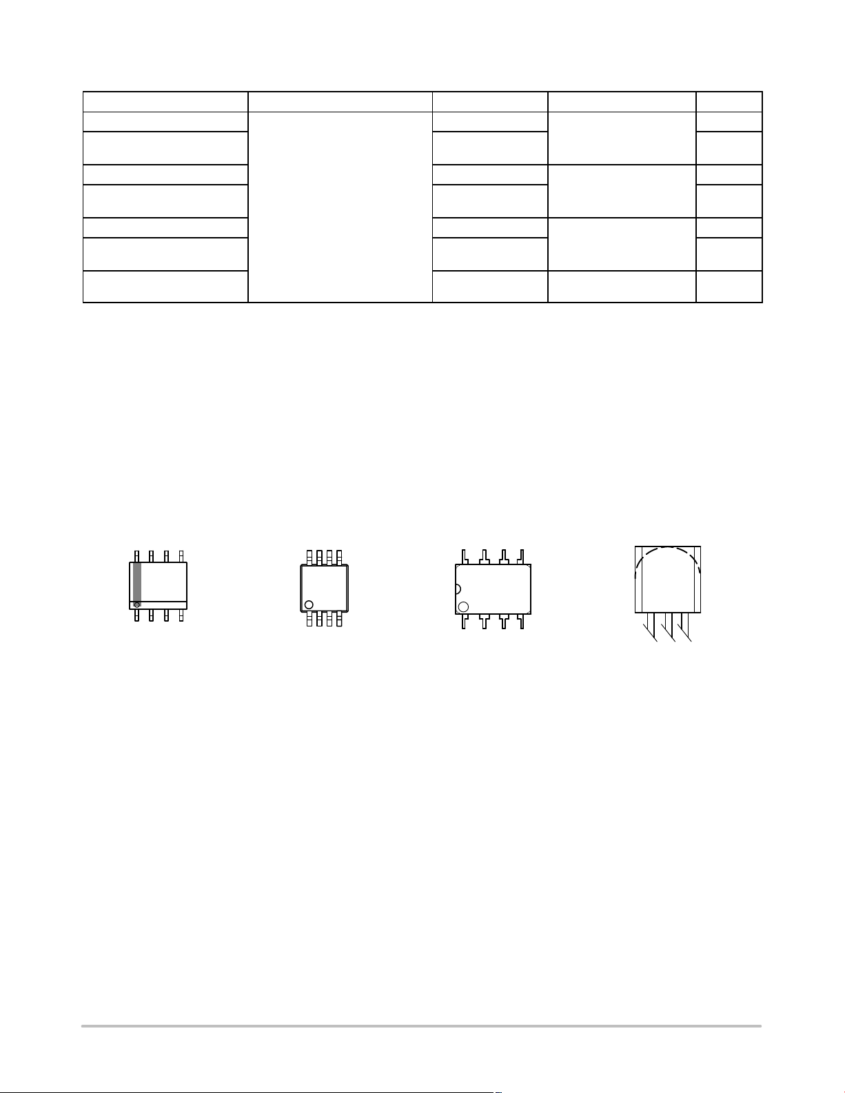
TL431, A, B Series, NCV431A, B
ORDERING INFORMATION
Device Operating Temperature Range Package Code Shipping Information
TL431BVP
TL431BVPG
NCV431AIDMR2
NCV431AIDMR2G
-40 °C to 125°C
NCV431AIDR2
NCV431AIDR2G
NCV431BVDMR2G
†For information on tape and reel specifications, including part orientation and tape sizes, please refer to our Tape and Reel Packaging
Specifications Brochure, BRD8011/D.
PDIP-8
PDIP-8
(Pb-Free)
Micro8
Micro8
(Pb-Free)
SOIC-8
SOIC-8
(Pb-Free)
Micro8
(Pb-Free)
50 Units / Rail
4000 Units / Tape & Reel
2500 Units / Tape & Reel
4000 Units / Tape & Reel 0.4%
MARKING DIAGRAMS
†
Tolerance
0.4%
0.4%
1%
1%
1%
1%
SOIC-8
D SUFFIX
CASE 751
8
431xx
ALYW
1
Micro8
CASE 846A
8
xxx
G
AYW G
G
1
xxxx = Specific Device Code
A = Assembly Location
Y, YY = Year
WW, W = Work Week
G or G = Pb-Free Package
(Note: Microdot may be in either location)
PDIP-8
CASE 626
8
TL431xx
AWL
YYWWG
1
TO-92 (TO-226)
CASE 29
TL431
xxxx
YWWG
G
http://onsemi.com
16
Page 17
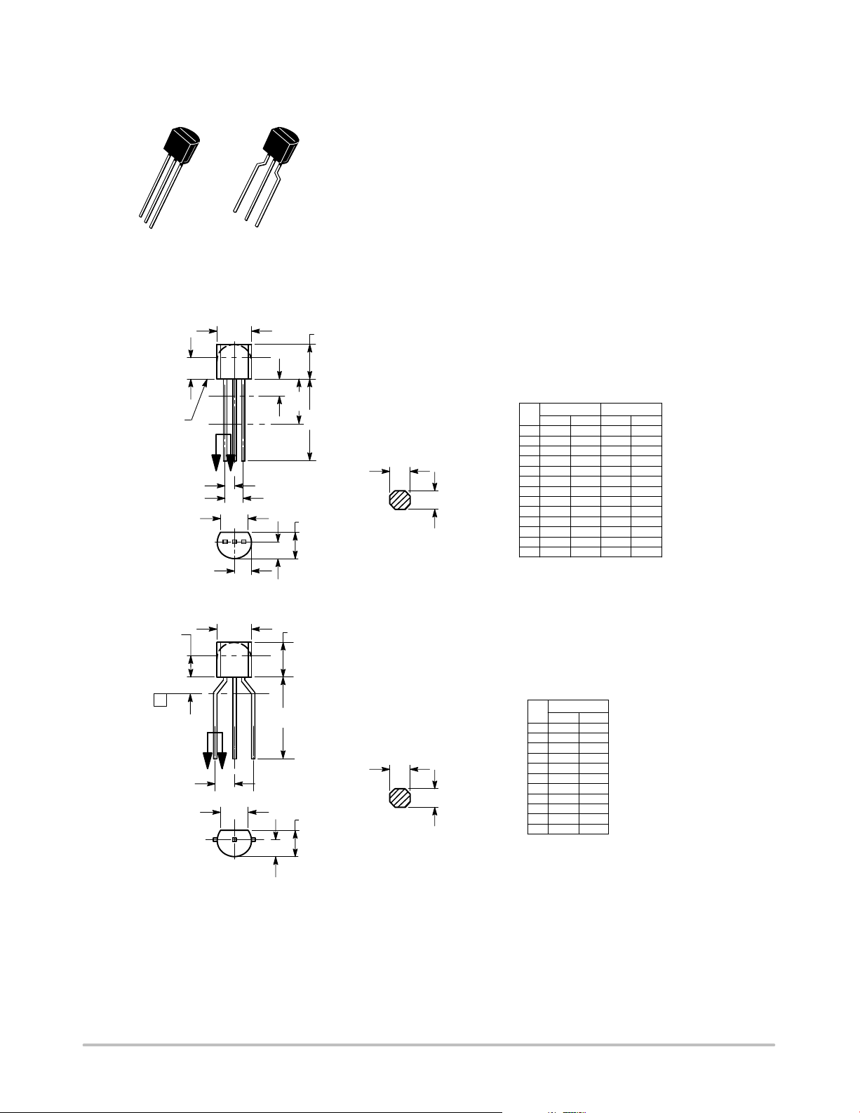
TL431, A, B Series, NCV431A, B
PACKAGE DIMENSIONS
TO-92 (TO-226)
CASE 29-11
ISSUE AM
1
2
3
STRAIGHT LEAD
BULK PACK
SEATING
PLANE
R
T
SEATING
PLANE
G
R
P
XX
XX
1
2
3
BENT LEAD
TAPE & REEL
AMMO PACK
A
G
H
V
1
N
A
V
1
B
STRAIGHT LEAD
BULK PACK
P
L
K
D
J
C
SECTION X-X
N
B
BENT LEAD
TAPE & REEL
AMMO PACK
K
D
J
C
SECTION X-X
NOTES:
1. DIMENSIONING AND TOLERANCING PER ANSI
Y14.5M, 1982.
2. CONTROLLING DIMENSION: INCH.
3. CONTOUR OF PACKAGE BEYOND DIMENSION R
IS UNCONTROLLED.
4. LEAD DIMENSION IS UNCONTROLLED IN P AND
BEYOND DIMENSION K MINIMUM.
DIM MIN MAX MIN MAX
A 0.175 0.205 4.45 5.20
B 0.170 0.210 4.32 5.33
C 0.125 0.165 3.18 4.19
D 0.016 0.021 0.407 0.533
G 0.045 0.055 1.15 1.39
H 0.095 0.105 2.42 2.66
J 0.015 0.020 0.39 0.50
K 0.500 --- 12.70 ---
L 0.250 --- 6.35 ---
N 0.080 0.105 2.04 2.66
P --- 0.100 --- 2.54
R 0.115 --- 2.93 ---
V 0.135 --- 3.43 ---
NOTES:
1. DIMENSIONING AND TOLERANCING PER
ASME Y14.5M, 1994.
2. CONTROLLING DIMENSION: MILLIMETERS.
3. CONTOUR OF PACKAGE BEYOND
DIMENSION R IS UNCONTROLLED.
4. LEAD DIMENSION IS UNCONTROLLED IN P
AND BEYOND DIMENSION K MINIMUM.
MILLIMETERS
DIM MIN MAX
A 4.45 5.20
B 4.32 5.33
C 3.18 4.19
D 0.40 0.54
G 2.40 2.80
J 0.39 0.50
K 12.70 ---
N 2.04 2.66
P 1.50 4.00
R 2.93 ---
V 3.43 ---
MILLIMETERSINCHES
N
http://onsemi.com
17
Page 18
NOTE 2
-T-
SEATING
PLANE
H
58
-B-
14
F
-A-
C
N
D
G
0.13 (0.005) B
TL431, A, B Series, NCV431A, B
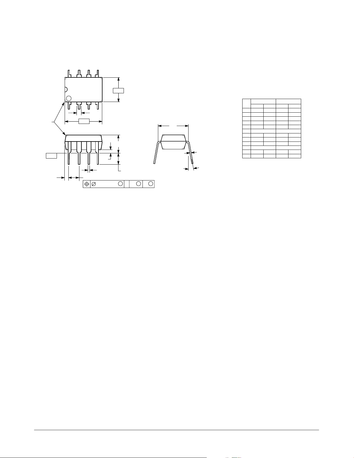
PDIP-8
P SUFFIX
PLASTIC PACKAGE
CASE 626-05
ISSUE L
L
J
K
M
M
A
T
M
M
NOTES:
1. DIMENSION L TO CENTER OF LEAD WHEN
FORMED PARALLEL.
2. PACKAGE CONTOUR OPTIONAL (ROUND OR
SQUARE CORNERS).
3. DIMENSIONING AND TOLERANCING PER ANSI
Y14.5M, 1982.
DIM MIN MAX MIN MAX
A 9.40 10.16 0.370 0.400
B 6.10 6.60 0.240 0.260
C 3.94 4.45 0.155 0.175
D 0.38 0.51 0.015 0.020
F 1.02 1.78 0.040 0.070
G 2.54 BSC 0.100 BSC
H 0.76 1.27 0.030 0.050
J 0.20 0.30 0.008 0.012
K 2.92 3.43 0.115 0.135
L 7.62 BSC 0.300 BSC
M --- 10 --- 10
N 0.76 1.01 0.030 0.040
INCHESMILLIMETERS
__
http://onsemi.com
18
Page 19
-T-
0.038 (0.0015)
PIN 1 ID
SEATING
PLANE
TL431, A, B Series, NCV431A, B
PACKAGE DIMENSIONS
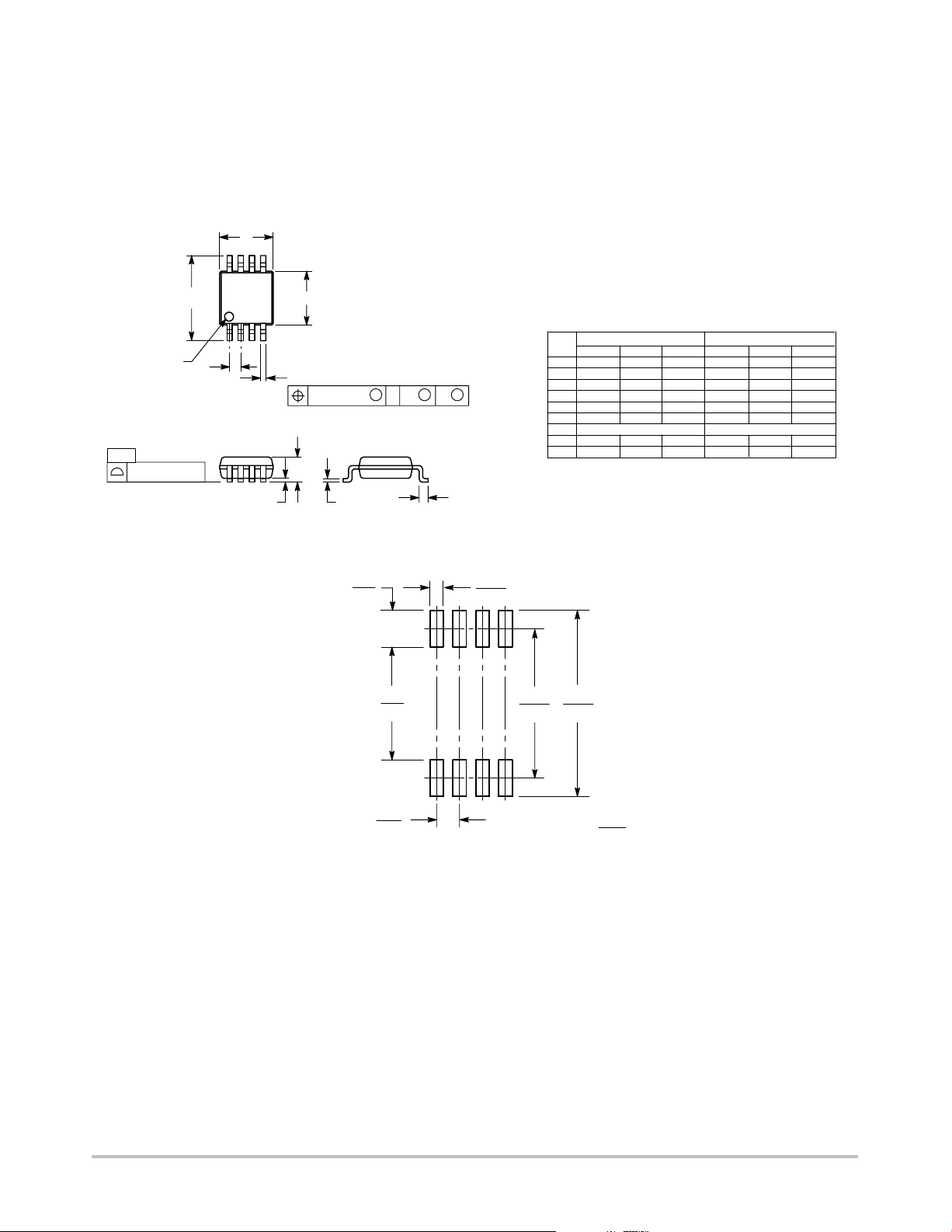
Micro8
DM SUFFIX
PLASTIC PACKAGE
CASE 846A-02
ISSUE G
DD
H
E
e
E
8 PL
b
0.08 (0.003) A
M
T
S
B
S
A
NOTES:
1. DIMENSIONING AND TOLERANCING PER ANSI Y14.5M, 1982.
2. CONTROLLING DIMENSION: MILLIMETER.
3. DIMENSION A DOES NOT INCLUDE MOLD FLASH, PROTRUSIONS OR GATE
BURRS. MOLD FLASH, PROTRUSIONS OR GATE BURRS SHALL NOT EXCEED
0.15 (0.006) PER SIDE.
4. DIMENSION B DOES NOT INCLUDE INTERLEAD FLASH OR PROTRUSION.
INTERLEAD FLASH OR PROTRUSION SHALL NOT EXCEED 0.25 (0.010) PER SIDE.
5. 846A-01 OBSOLETE, NEW STANDARD 846A-02.
DIMAMIN NOM MAX MIN
A1 0.05 0.08 0.15 0.002
b 0.25 0.33 0.40 0.010
c 0.13 0.18 0.23 0.005
D 2.90 3.00 3.10 0.114
E 2.90 3.00 3.10 0.114
e 0.65 BSC
L 0.40 0.55 0.70 0.016
H
MILLIMETERS
-- -- 1.10 --
4.75 4.90 5.05 0.187 0.193 0.199
E
INCHES
NOM MAX
-- 0.043
0.003 0.006
0.013 0.016
0.007 0.009
0.118 0.122
0.118 0.122
0.026 BSC
0.021 0.028
A1
c
L
SOLDERING FOOTPRINT*
1.04
8X
0.041
3.20
0.126
0.65
6X
0.0256
*For additional information on our Pb-Free strategy and soldering
details, please download the ON Semiconductor Soldering and
Mounting Techniques Reference Manual, SOLDERRM/D.
0.38
0.015
8X
4.24
0.167
SCALE 8:1
5.28
0.208
ǒ
inches
mm
Ǔ
http://onsemi.com
19
Page 20
-Z-
-Y-
TL431, A, B Series, NCV431A, B
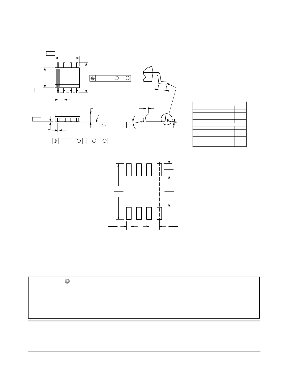
SOIC-8
D SUFFIX
PLASTIC PACKAGE
CASE 751-07
ISSUE AH
-XA
58
B
1
S
0.25 (0.010)
4
M
M
Y
K
G
C
SEATING
PLANE
0.10 (0.004)
H
D
0.25 (0.010) Z
M
SXS
Y
N
X 45
_
M
J
NOTES:
1. DIMENSIONING AND TOLERANCING PER
ANSI Y14.5M, 1982.
2. CONTROLLING DIMENSION: MILLIMETER.
3. DIMENSION A AND B DO NOT INCLUDE
MOLD PROTRUSION.
4. MAXIMUM MOLD PROTRUSION 0.15 (0.006)
PER SIDE.
5. DIMENSION D DOES NOT INCLUDE DAMBAR
PROTRUSION. ALLOWABLE DAMBAR
PROTRUSION SHALL BE 0.127 (0.005) TOTAL
IN EXCESS OF THE D DIMENSION AT
MAXIMUM MATERIAL CONDITION.
6. 751-01 THRU 751-06 ARE OBSOLETE. NEW
STANDARD IS 751-07.
MILLIMETERS
DIMAMIN MAX MIN MAX
4.80 5.00 0.189 0.197
B 3.80 4.00 0.150 0.157
C 1.35 1.75 0.053 0.069
D 0.33 0.51 0.013 0.020
G 1.27 BSC 0.050 BSC
H 0.10 0.25 0.004 0.010
J 0.19 0.25 0.007 0.010
K 0.40 1.27 0.016 0.050
M 0 8 0 8
____
N 0.25 0.50 0.010 0.020
S 5.80 6.20 0.228 0.244
INCHES
SOLDERING FOOTPRINT*
1.52
0.060
7.0
0.275
0.6
0.024
*For additional information on our Pb-Free strategy and soldering
details, please download the ON Semiconductor Soldering and
Mounting Techniques Reference Manual, SOLDERRM/D.
Micro8 is a trademark of International Rectifier.
ON Semiconductor and are registered trademarks of Semiconductor Components Industries, LLC (SCILLC). SCILLC reserves the right to make changes without further notice
to any products herein. SCILLC makes no warranty, representation or guarantee regarding the suitability of its products for any particular purpose, nor does SCILLC assume any liability
arising out of the application or use of any product or circuit, and specifically disclaims any and all liability, including without limitation special, consequential or incidental damages.
“Typical” parameters which may be provided in SCILLC data sheets and/or specifications can and do vary in different applications and actual performance may vary over time. All
operating parameters, including “Typicals” must be validated for each customer application by customer's technical experts. SCILLC does not convey any license under its patent rights
nor the rights of others. SCILLC products are not designed, intended, or authorized for use as components in systems intended for surgical implant into the body, or other applications
intended to support or sustain life, or for any other application in which the failure of the SCILLC product could create a situation where personal injury or death may occur. Should
Buyer purchase or use SCILLC products for any such unintended or unauthorized application, Buyer shall indemnify and hold SCILLC and its officers, employees, subsidiaries, affiliates,
and distributors harmless against all claims, costs, damages, and expenses, and reasonable attorney fees arising out of, directly or indirectly, any claim of personal injury or death
associated with such unintended or unauthorized use, even if such claim alleges that SCILLC was negligent regarding the design or manufacture of the part. SCILLC is an Equal
Opportunity/Affirmative Action Employer. This literature is subject to all applicable copyright laws and is not for resale in any manner.
4.0
0.155
1.270
0.050
SCALE 6:1
ǒ
inches
mm
Ǔ
PUBLICATION ORDERING INFORMATION
LITERATURE FULFILLMENT:
Literature Distribution Center for ON Semiconductor
P.O. Box 5163, Denver, Colorado 80217 USA
Phone: 303-675-2175 or 800-344-3860 Toll Free USA/Canada
Fax: 303-675-2176 or 800-344-3867 Toll Free USA/Canada
Email: [email protected]
N. American Technical Support: 800-282-9855 Toll Free
USA/Canada
Europe, Middle East and Africa Technical Support:
Phone: 421 33 790 2910
Japan Customer Focus Center
Phone: 81-3-5773-3850
http://onsemi.com
20
ON Semiconductor Website: www.onsemi.com
Order Literature: http://www.onsemi.com/orderlit
For additional information, please contact your local
Sales Representative
TL431/D
 Loading...