

Page 1
TL2218-285, TL2218-285Y
EXCALIBUR CURRENT-MODE SCSI TERMINATOR
SLVS072C – DECEMBER 1992 – REVISED OCTOBER 1995
POST OFFICE BOX 655303 • DALLAS, TEXAS 75265
Copyright 1995, Texas Instruments Incorporated
8–1
available features
• Fully Integrated 9-Channel SCSI
Termination
• No External Components Required
• Maximum Allowed Current Applied at First
High-Level Step
• 6-pF Typical Power-Down Output
Capacitance
• Wide V
term
†
(Termination Voltage)
Operating Range, 3.5 V to 5.5 V
• TTL-Compatible Disable Feature
• Compatible With Active Negation
• Thermal Regulation
description
The TL2218-285 is a current-mode 9-channel monolithic terminator specially designed for single-ended
small-computer-systems-interface (SCSI) bus termination. A user-controlled disable function is provided to
reduce standby power. No impedance-matching resistors or other external components are required for its
operation as a complete terminator.
The device operates over a wide termination-voltage (V
term
†
) range of 3.5 V to 5.5 V , offering an extra 0.5 V of
operating range when compared to the minimum termination voltage of 4 V required by other integrated active
terminators. The TL2218-285 functions as a current-sourcing terminator and supplies a constant output current
of 23 mA into each asserted line. When a line is deasserted, the device senses the rising voltage level and begins
to function as a voltage source, supplying a fixed output voltage of 2.85 V. The TL2218-285 features
compatibility with active negation drivers and has a typical sink current capability of 20 mA.
The TL2218-285 is able to ensure that maximum current is applied at the first high-level step. This performance
means that the device should provide a first high-level step exceeding 2 V even at a 10-MHz rate. Therefore,
noise margins are improved considerably above those provided by resistive terminators.
A key difference between the TL2218-285 current-mode terminator and a Boulay terminator is that the
TL2218-285 does not incorporate a low dropout regulator to set the output voltage to 2.85 V. In contrast with
the Boulay termination concept, the accuracy of the 2.85 V is not critical with the current-mode method used
in the TL2218-285 because this voltage does not determine the driver current. Therefore, the primary device
specifications are not the same as with a voltage regulator but are more concerned with output current.
The DISABLE
terminal is TTL compatible and must be taken low to shut down the outputs. The device is
normally active, even when DISABLE
is left floating. In the disable mode, only the device startup circuits remain
active, thereby reducing the supply current to just 500 µA. Output capacitance in the shutdown mode is typically
6 pF.
The TL2218-285 has on-board thermal regulation and current limiting, thus eliminating the need for external
protection circuitry . A thermal regulation circuit that is designed to provide current limiting, rather than an actual
thermal shutdown, is included in the individual channels of the TL2218-285. When a system fault occurs that
leads to excessive power dissipation by the terminator, the thermal regulation circuit causes a reduction in the
asserted-line output current sufficient to maintain operation. This feature allows the bus to remain active during
a fault condition, which permits data transfer immediately upon removal of the fault. A terminator with thermal
shutdown does not allow for data transfer until sufficient cooling has occurred. Another advantage offered by
the TL2218-285 is a design that does not require costly laser trimming in the manufacturing process.
The TL2218-285 is characterized for operation over the virtual junction temperature range of 0°C to 125°C.
†
This symbol is not presently listed within EIA/JEDEC standards for letter symbols.
2
3
4
5
6
7
8
9
10
20
19
18
17
16
15
14
13
12
11
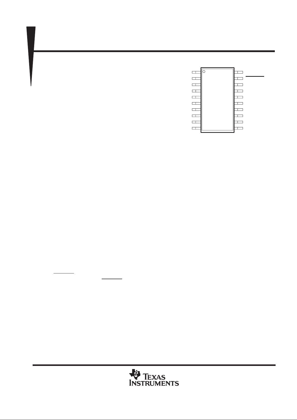
TERMPWR
NC
NC
D0
D1
D2
D3
D4
NC
GND
TERMPWR
DISABLE
NC
D8
D7
NC
D6
D5
NC
GND
PW PACKAGE
(TOP VIEW)
1
NC – No internal connection
PRODUCTION DATA information is current as of publication date.
Products conform to specifications per the terms of Texas Instruments
standard warranty. Production processing does not necessarily include
testing of all parameters.
Page 2
TL2218-285, TL2218-285Y
EXCALIBUR CURRENT -MODE SCSI TERMINATOR
SLVS072C – DECEMBER 1992 – REVISED OCTOBER 1995
POST OFFICE BOX 655303 • DALLAS, TEXAS 75265
8–2
AVAILABLE OPTIONS
T
J
SURFACE MOUNT
(PW)
†
CHIP FORM
(Y)
0°C to 125°C TL2218-285PWLE TL2218-285Y
†
The PW package is only available left-end taped and reeled.
TL2218-285Y chip information
This chip, when properly assembled, displays characteristics similar to the TL2218-285. Thermal compression
or ultrasonic bonding may be used on the doped aluminum bonding pads. The chip may be mounted with
conductive epoxy or a gold-silicon preform.
BONDING PAD ASSIGNMENTS
CHIP THICKNESS: 11 MILS TYPICAL
BONDING PADS: 4 × 4 MILS MINIMUM
TJmax = 150°C
TOLERANCES ARE ±10%.
ALL DIMENSIONS ARE IN MILS.
Thermal
Regulation
Feedback
Active
Negation
Clamp
TERMPWR
1, 20
4
19
V
ref
DISABLE
D0
Common to All Channels
161
84
(1)
(4)
(5)
(6)
(7)
(8)
(10)(11)
(13)
(14)
(16)
(17)
(19)
(20)
Page 3
TL2218-285, TL2218-285Y
EXCALIBUR CURRENT -MODE SCSI TERMINATOR
SLVS072C – DECEMBER 1992 – REVISED OCTOBER 1995
POST OFFICE BOX 655303 • DALLAS, TEXAS 75265
8–3
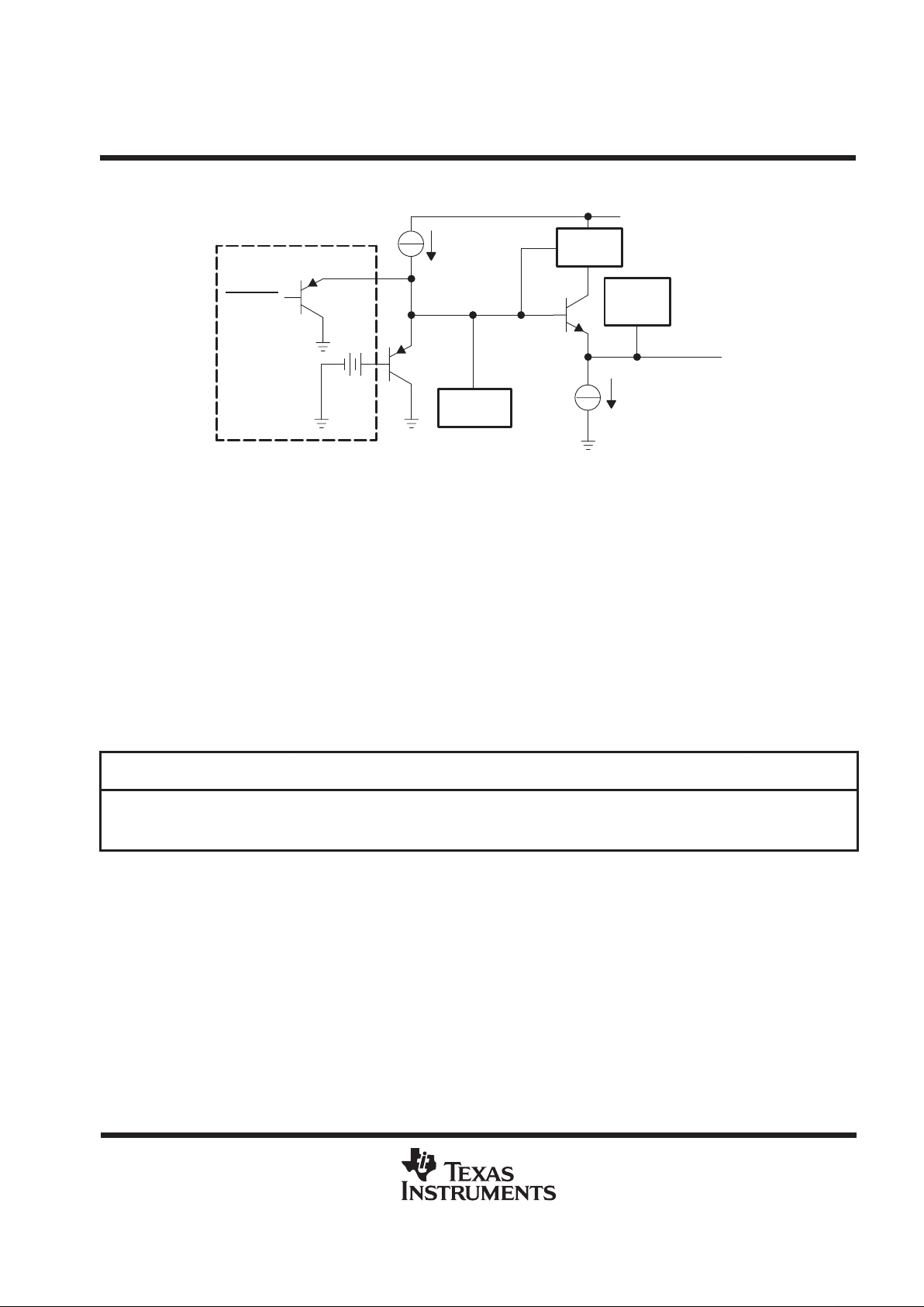
functional block diagram (each channel)
Thermal
Regulation
Feedback
Active
Negation
Clamp
TERMPWR
1, 20
4
19
V
ref
DISABLE
D0
Common to All Channels
absolute maximum ratings over operating free-air temperature range (unless otherwise noted)
(see Figures 1, 2, and 3)
†
Continuous termination voltage 10 V. . . . . . . . . . . . . . . . . . . . . . . . . . . . . . . . . . . . . . . . . . . . . . . . . . . . . . . . . . . . .
Continuous output voltage range 0 V to 5.5 V. . . . . . . . . . . . . . . . . . . . . . . . . . . . . . . . . . . . . . . . . . . . . . . . . . . . . .
Continuous disable voltage range 0 V to 5.5 V. . . . . . . . . . . . . . . . . . . . . . . . . . . . . . . . . . . . . . . . . . . . . . . . . . . . .
Continuous total power dissipation See Dissipation Rating Table. . . . . . . . . . . . . . . . . . . . . . . . . . . . . . . . . . . . .
Operating virtual junction temperature range, T
J
–55°C to 150°C. . . . . . . . . . . . . . . . . . . . . . . . . . . . . . . . . . . .
Storage temperature range, T
stg
–60°C to 150°C. . . . . . . . . . . . . . . . . . . . . . . . . . . . . . . . . . . . . . . . . . . . . . . . . .
Lead temperature 1,6 mm (1/16 inch) from case for 10 seconds 260°C. . . . . . . . . . . . . . . . . . . . . . . . . . . . . . .
†
Stresses beyond those listed under “absolute maximum ratings” may cause permanent damage to the device. These are stress ratings only, and
functional operation of the device at these or any other conditions beyond those indicated under “recommended operating conditions” is not
implied. Exposure to absolute-maximum-rated conditions for extended periods may affect device reliability.
DISSIPATION RATING TABLE
POWER RATING T ≤ 25°C DERATING FACTOR T = 70°C T = 85°C T = 125°C
PACKAGE
AT POWER RATING ABOVE T = 25°C POWER RATING POWER RATING POWER RATING
T
A
828 mW 6.62 mW/°C 530 mW 430 mW 166 mW
PW
T
C
4032 mW 32.2 mW/°C 2583 mW 2100 mW 812 mW
T
L
‡
2475 mW 19.8 mW/°C 1584 mW 1287 mW 495 mW
‡
R
θJL
is the thermal resistance between the junction and device lead. T o determine the virtual junction temperature (TJ) relative to the device lead
temperature, the following calculations should be used: TJ = PD x R
θJL
+ TL, where PD is the internal power dissipation of the device and TL is
the device lead temperature at the point of contact to the printed wiring board. R
θJL
is 50.5°C/W.
Page 4

TL2218-285, TL2218-285Y
EXCALIBUR CURRENT -MODE SCSI TERMINATOR
SLVS072C – DECEMBER 1992 – REVISED OCTOBER 1995
POST OFFICE BOX 655303 • DALLAS, TEXAS 75265
8–4
600
400
200
0
25 50 75 100
800
1000
1200
125 150
1800
1600
1400
2000
2200
2400
FREE-AIR TEMPERATURE
DISSIPATION DERATING CURVE
TA – Free-Air Temperature – °C
Maximum Continuous Power Dissipation – mW
1200
800
400
0
25 50 75 100
1600
2000
2400
125 150
3600
3200
2800
4000
4400
4800
CASE TEMPERATURE
DISSIPATION DERATING CURVE
TC – Case Temperature – ° C
R
θJA
= 151°C/W
R
θJC
= 31°C/W
Maximum Continuous Power Dissipation – mW
Figure 1 Figure 2
1200
800
400
0
25 50 75 100
2000
125 150
3600
3200
2800
4000
4400
4800
LEAD TEMPERATURE
DISSIPATION DERATING CURVE
TL – Lead Temperature – ° C
2400
1600
†
R
θJL
= 50.5°C/W
Maximum Continuous Power Dissipation – mW
Figure 3
†
R
θJL
is the thermal resistance between the junction and device lead. T o determine the virtual junction temperature (TJ) relative to the device lead
temperature, the following calculations should be used: TJ = PD x R
θJL
+ TL, where PD is the internal power dissipation of the device, and TL is
the device lead temperature at the point of contact to the printed wiring board. R
θJL
is 50.5°C/W.
Page 5

TL2218-285, TL2218-285Y
EXCALIBUR CURRENT -MODE SCSI TERMINATOR
SLVS072C – DECEMBER 1992 – REVISED OCTOBER 1995
POST OFFICE BOX 655303 • DALLAS, TEXAS 75265
8–5
recommended operating conditions
MIN MAX UNIT
Termination voltage 3.5 5.5 V
High-level disable input voltage, V
IH
2 V
term
V
Low-level disable input voltage, V
IL
0 0.8 V
Operating virtual junction temperature, T
J
0 125 °C
electrical characteristics, V
term
= 4.75 V, VO = 0.5 V, TJ = 25°C
PARAMETER TEST CONDITIONS MIN TYP MAX UNIT
Output high voltage 2.5 2.85 V
All data lines open 9
TERMPWR supply current
All data lines = 0.5 V 228
mA
DISABLE = 0 V 500 µA
Output current –20.5 –23 –24 mA
p
DISABLE = 4.75 V 1
Disable input current (see Note 1)
DISABLE = 0 V 600
µ
A
Output leakage current DISABLE = 0 V 100 nA
Output capacitance, device disabled VO = 0 V, 1 MHz 6 pF
Termination sink current, total VO = 4 V 20 mA
NOTE 1: When DISABLE is open or high, the terminator is active.
Page 6

TL2218-285, TL2218-285Y
EXCALIBUR CURRENT -MODE SCSI TERMINATOR
SLVS072C – DECEMBER 1992 – REVISED OCTOBER 1995
POST OFFICE BOX 655303 • DALLAS, TEXAS 75265
8–6
THERMAL INFORMATION
The need for smaller surface-mount packages for use on compact printed-wiring boards (PWB) causes an
increasingly difficult problem in the area of thermal dissipation. In order to provide the systems designer with a better
approximation of the junction temperature rise in the thin-shrink small-outline package (TSSOP), the junction-to-lead
thermal resistance (R
θJL
) is provided along with the more typical values of junction-to-ambient and junction-to-case
thermal resistances, R
θJA
and R
θJC
.
R
θJL
is used to calculate the device junction temperature rise measured from the leads of the unit. Consequently , the
junction temperature is dependent upon the board temperature at the leads, R
θJL
, and the internal power dissipation
of the device. The board temperature is contingent upon several variables, including device packing density,
thickness, material, area, and number of interconnects. The R
θJL
value depends on the number of leads connecting
to the die-mount pad, the lead-frame alloy , area of the die, mount material, and mold compound. Since the power level
at which the TSSOP can be used is highly dependent upon both the temperature rise of the PWB and the device itself,
the systems designer can maximize this level by optimizing the circuit board. The junction temperature of the device
can be calculated using the equation T
J
= (PD × R
θJL
) + TL where TJ = junction temperature, PD = power dissipation,
R
θJL
= junction-to-lead thermal resistance, and TL = board temperature at the leads of the unit.
The values of thermal resistance for the TL2218-285 PW are as follows:
Thermal Resistance Typical Junction Rise
R
θJA
151°C/W
R
θJC
31 °C/W
R
θJL
50.5°C/W
TYPICAL CHARACTERISTICS
Table of Graphs
FIGURE
I
O
Output current vs Input voltage 4
V
O
Output voltage vs Input voltage 5
I
O
Output current vs Junction temperature 6
V
O
Output voltage vs Junction temperature 7
Page 7

TL2218-285, TL2218-285Y
EXCALIBUR CURRENT -MODE SCSI TERMINATOR
SLVS072C – DECEMBER 1992 – REVISED OCTOBER 1995
POST OFFICE BOX 655303 • DALLAS, TEXAS 75265
8–7
TYPICAL CHARACTERISTICS
20
18
16
14
3 3.5 4 4.5
– Output Current – mA
22
OUTPUT CURRENT
vs
INPUT VOLTAGE
24
5 5.5
TJ = 25°C
VI – Input Voltage – V
2
1
0
3 3.5 4 4.5
VO – Output Voltage – V
OUTPUT VOLTAGE
vs
INPUT VOLTAGE
4
5 5.5
3
TJ = 25°C
V
O
VI – Input Voltage – V
I
O
Figure 4 Figure 5
15
10
5
0255075
20
OUTPUT CURRENT
vs
JUNCTION TEMPERATURE
25
100 125
V
term
= 4.75 V
TA = T
J
TJ – Junction Temperature – °C
3
2.5
2
0255075
3.5
4
100 125
V
term
= 4.75 V
TA = T
J
VO – Output Voltage – V
V
O
TJ – Junction Temperature – °C
OUTPUT VOLTAGE
vs
JUNCTION TEMPERATURE
– Output Current – mA
I
O
Figure 6 Figure 7
Page 8

POST OFFICE BOX 655303 • DALLAS, TEXAS 75265
8–8
Page 9

IMPORTANT NOTICE
T exas Instruments and its subsidiaries (TI) reserve the right to make changes to their products or to discontinue
any product or service without notice, and advise customers to obtain the latest version of relevant information
to verify, before placing orders, that information being relied on is current and complete. All products are sold
subject to the terms and conditions of sale supplied at the time of order acknowledgement, including those
pertaining to warranty, patent infringement, and limitation of liability.
TI warrants performance of its semiconductor products to the specifications applicable at the time of sale in
accordance with TI’s standard warranty. Testing and other quality control techniques are utilized to the extent
TI deems necessary to support this warranty. Specific testing of all parameters of each device is not necessarily
performed, except those mandated by government requirements.
CERT AIN APPLICATIONS USING SEMICONDUCTOR PRODUCTS MAY INVOLVE POTENTIAL RISKS OF
DEATH, PERSONAL INJURY, OR SEVERE PROPERTY OR ENVIRONMENTAL DAMAGE (“CRITICAL
APPLICATIONS”). TI SEMICONDUCTOR PRODUCTS ARE NOT DESIGNED, AUTHORIZED, OR
WARRANTED TO BE SUITABLE FOR USE IN LIFE-SUPPORT DEVICES OR SYSTEMS OR OTHER
CRITICAL APPLICATIONS. INCLUSION OF TI PRODUCTS IN SUCH APPLICA TIONS IS UNDERST OOD TO
BE FULLY AT THE CUSTOMER’S RISK.
In order to minimize risks associated with the customer’s applications, adequate design and operating
safeguards must be provided by the customer to minimize inherent or procedural hazards.
TI assumes no liability for applications assistance or customer product design. TI does not warrant or represent
that any license, either express or implied, is granted under any patent right, copyright, mask work right, or other
intellectual property right of TI covering or relating to any combination, machine, or process in which such
semiconductor products or services might be or are used. TI’s publication of information regarding any third
party’s products or services does not constitute TI’s approval, warranty or endorsement thereof.
Copyright 1998, Texas Instruments Incorporated
 Loading...