

Page 1
TL16PC564B, TL16PC564BLV
PCMCIA UNIVERSAL ASYNCHRONOUS RECEIVER TRANSMITTER
SLLS225A – MARCH 1996 – REVISED FEBRUARY 1998
D
Integrated Asynchronous Communications
Element (ACE) Compatible With PCMCIA
PC Card Standard Release 2.01
D
Consists of a Single TL16C550 ACE Plus
PCMCIA Interface Logic
D
Provides Common I-Bus/Z-Bus
Microcontroller Inputs for Most Intel
Zilog
D
Fully Programmable 256-Byte Card
Subsystems
and
Information Structure (CIS) and 8-Byte Card
Configuration Register (CCR)
D
Adds or Deletes Standard Asynchronous
Communication Bits (Start, Stop and
Parity) to or From Serial Data Stream
D
Independently Controlled Transmit,
Receive, Line Status, and Data Set
Interrupts
D
Subsystem Selectable Serial-Bypass Mode
Provides Subsystem With Direct Parallel
Access to the FIFOs
description
The TL16PC564B/BL V† is designed to provide all the functions necessary for a Personal Computer Memory
Card International Association (PCMCIA) universal asynchronous receiver transmitter (UART) subsystem
interface. This interface provides a serial-to-parallel conversion for data to and from a modem
coder-decoder/digital signal processor (CODEC/DSP) function to a PCMCIA parallel data-port format. A
computer central processing unit (CPU), through a PCMCIA host controller, can read the status of the
asynchronous communications element (ACE) interface at any point in the operation. Reported status
information includes the type of transfer operation in process, the status of the operation, and any error
conditions encountered.
Attribute memory consists of a 256-byte card information structure (CIS) and eight 8-byte card configuration
registers (CCR). The CIS, implemented with a dual-port random-access memory (DPRAM), is available to both
the host CPU and subsystem (modem), as are the CCRs. This DPRAM is used in place of the electrically
erasable programmable read-only memory (EEPROM) normally used for the CIS. At power up, attribute
memory is initialized by the subsystem.
The TL16PC564B/BLV uses a TL16C550 ACE-type core with an expanded 64 × 11 receiver first-in-first-out
(FIFO) memory and a 64 × 8 transmitter FIFO memory . The receiver trigger logic flags have been adjusted in
order to take full advantage of the increased capacity when in the extended mode. In addition, eight of the UART
registers have been mapped into the subsystem (modem) memory space as read-only registers. This allows
the subsystem to read UART status information.
D
Fully Programmable Serial-Interface
Characteristics:
– 5-, 6-, 7-, or 8-Bit Characters
– Even-, Odd-, or No-Parity Bit Generation
and Detection
– 1-, 1 1/2-, or 2-Stop Bit Generation
– Baud-Rate Generation
D
Fully Prioritized Interrupt System Controls
D
Modem Control Functions
D
Provides TL16C450 Mode at Reset Plus
Selectable Normal TL16C550 Operation or
Extended 64-Byte FIFO Mode
D
Selectable Auto-RTS Mode Deactivates
RTS
at 14 Bytes in 550 Mode and at
56 Bytes in Extended 550 Mode
D
Selectable Auto-CTS Mode Deactivates
Serial Transfers When CTS
D
Available in 100 Pin Thin Quad Flatpack
is Inactive
(PZ) Package
A subsystem-selectable serial-bypass mode has been implemented to allow the subsystem to bypass the serial
portion of the UART and write directly to the receiver FIFO and read directly from the transmitter FIFO. Interrupt
operation is not affected in this mode.
Please be aware that an important notice concerning availability, standard warranty, and use in critical applications of
Texas Instruments semiconductor products and disclaimers thereto appears at the end of this data sheet.
Intel is a registered trademark of Intel System, Inc.
Zilog is a registered trademark of Zilog Incorporated
†
Patent pending
PRODUCTION DATA information is current as of publication date.
Products conform to specifications per the terms of Texas Instruments
standard warranty. Production processing does not necessarily include
testing of all parameters.
POST OFFICE BOX 655303 • DALLAS, TEXAS 75265
Copyright 1998, Texas Instruments Incorporated
1
Page 2
TL16PC564B, TL16PC564BLV
PCMCIA UNIVERSAL ASYNCHRONOUS RECEIVER TRANSMITTER
SLLS225A – MARCH 1996 – REVISED FEBRUARY 1998
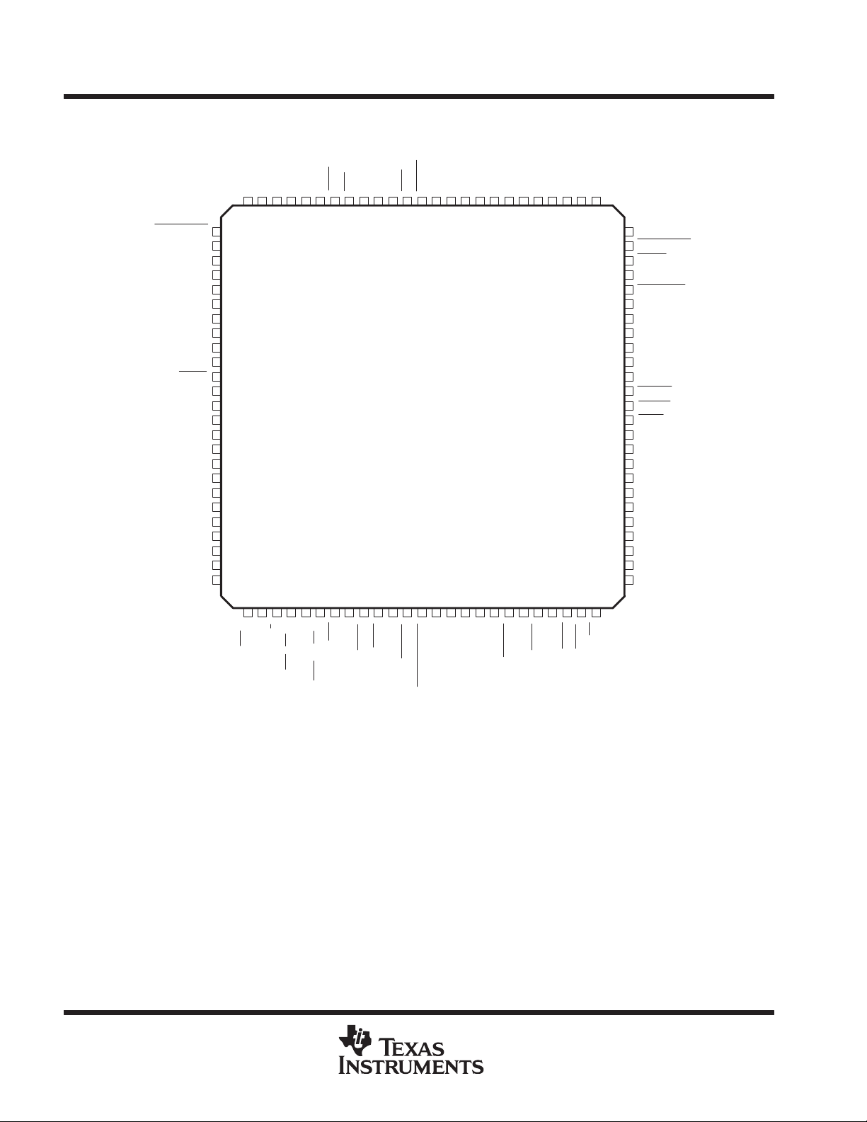
PZ PACKAGE
(TOP VIEW)
EXTEND
VTEST
SSAB
GND
ARBCLKI
GND
ARBCLKO
ARBPGM0
ARBPGM1
V
CC
RST
NANDOUT
GND
SAD7
SAD6
GND
SAD5
SAD4
SAD3
SAD2
V
CC
V
CC
SAD1
SA8
SAD0
1
2
3
4
5
6
7
8
9
10
11
12
13
14
15
16
17
18
19
20
21
22
23
24
25
HD3
100
26
HD4
99
27
HD5
98
28
V
97
29
CC
HD6
96
30
HD7
CE1OEHA9
94
95
32
31
93
33
92
34
GND
HA8
90
91
36
35
WE
89
37
IREQ
HA7
87
88
39
38
CC
V
86
40
HA6
85
41
HA5
84
42
HA4
83
43
HA3
82
44
HA2
81
45
GND
HA1
79
80
47
46
HA0
78
48
HD0
77
49
HD1
76
75
74
73
72
71
70
69
68
67
66
65
64
63
62
61
60
59
58
57
56
55
54
53
52
51
50
HD2
STSCHG
REG
V
CC
INPACK
TESTOUT
GND
GND
RESET
GND
SA7
IOWR
IORD
CE2
SA6
V
CC
SA5
SA4
SA3
SA2
SA1
GND
SA0
V
CC
UARTCLK
†
IRQ
ALE (AS)
†
The terminal names not enclosed in parentheses correspond to an Intel microcontroller signal, and the terminal
names enclosed in parentheses correspond to a Zilog microcontroller signal.
†
SELZ/I
RD(DS)
†
GND
WR(R/W)
CS
SIN
DTR
RI
CC
RTS
V
OUT1
GND
RCLK
XIN
GND
GND
OUT2
DSR
SOUT
V
CC
CTS
DCD
BAUDOUT
2
POST OFFICE BOX 655303 • DALLAS, TEXAS 75265
Page 3
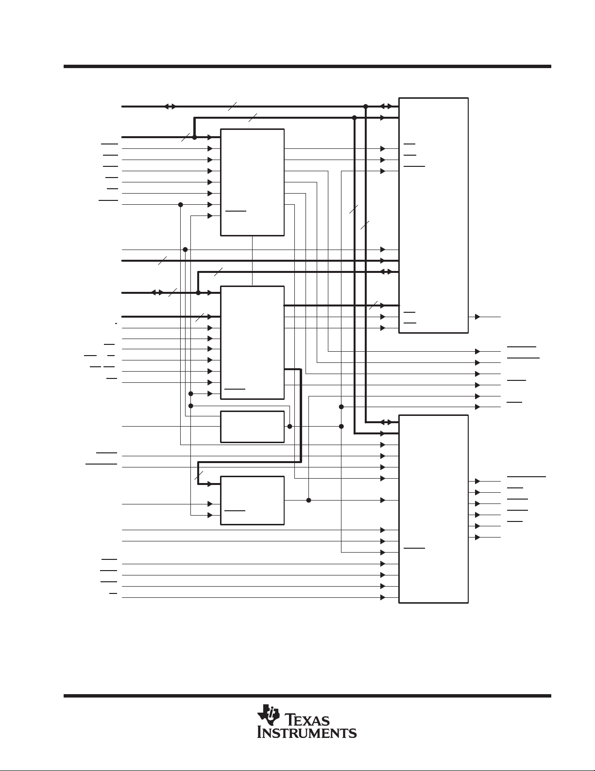
block diagram
TL16PC564B, TL16PC564BLV
PCMCIA UNIVERSAL ASYNCHRONOUS RECEIVER TRANSMITTER
SLLS225A – MARCH 1996 – REVISED FEBRUARY 1998
HD7–HD0
HA9–HA0
REG
CE1
CE2
WE
OE
IORD
ARBCLKI
ARBPGM1–
ARBPGM0
SAD7–SAD0
SA8–SA0
SELZ/I
SSAB
ALE(AS
(R/W)
WR
RD
(DS)
CS
RESET
95, 96, 98–100, 75–77
†
92, 90, 87, 85–81,
79, 78
†
73
94
62
89
93
63
5
9,8
†
14, 15, 17–20,
23, 25
†
24,65,61,
59–55,53
28
3
26
)
31
29
32
67
2
8
10
8
10
Host CPU
Control
Logic
10
Reset
Control
8
9
Subsystem
Control
Logic
Reset
Reset
Validation
8
9
DATA
ADDR
OE
WE
Reset
Attribute
Memory
(CIS 256 × 8,
CCR 8 × 8
plus arbitration
logic)
DATA
ADDR
OE
WE
7
71
74
27
88
51
11
ARBCLKO
INPACK
STSCHG
IRQ
IREQ
UARTCLK
RST
64
IOWR
XIN
SIN
RCLK
CTS
DCD
DSR
1
42
33
40
49
48
46
50
RI
EXTEND
†
Bit 0 is the least significant bit.
6
Divide by N
Reset
UART
TL16C550C
UART Select
Master Clock
Reset
38
34
37
44
35
45
BAUDOUT
DTR
OUT1
OUT2
RTS
SOUT
POST OFFICE BOX 655303 • DALLAS, TEXAS 75265
3
Page 4
TL16PC564B, TL16PC564BLV
INTER
I/O
DESCRIPTION
PCMCIA UNIVERSAL ASYNCHRONOUS RECEIVER TRANSMITTER
SLLS225A – MARCH 1996 – REVISED FEBRUARY 1998
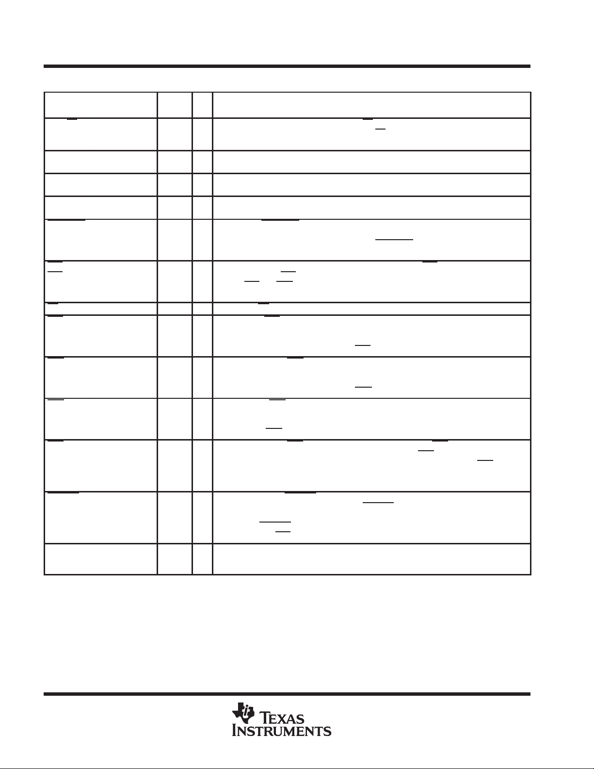
Terminal Functions
TERMINAL
NAME NO.
ALE (AS) 26 S I Address-latch enable/address strobe. ALE(AS) is an address-latch enable in the Intel mode
ARBCLKO 7 M O Arbitration clock output. ARBCLKO is equal to the input on ARBCLKI divided by the
ARBCLKI 5 M I Arbitration clock input. ARBCLKI is the base clock used in arbitration for the attribute memory
ARBPGM0
ARBPGM1
BAUDOUT 38 U O Baud output. BAUDOUT is an active-low 16× signal for the transmitter section of the UART.
CE1
CE2
CS 32 S I Chip select. CS is the active-low chip select from the Zilog or Intel microcontroller.
CTS 49 U I Clear to send. CTS is an active-low modem status signal whose condition can be checked by
DCD 48 U I Data carrier detect. DCD is an active-low modem-status signal whose condition can be
DSR 46 U I Data set ready. DSR is an active-low modem status signal whose condition can be checked
DTR 34 U O Data terminal ready. DSD is an active-low signal. When active, DTR informs the modem or
EXTEND 1 U I FIFO extend. When EXTEND is high, the UART is configured as a standard TL16C550 with
GND 4,6,13,16,30,
†
Host = H, Subsystem = S, UART = U, Miscellaneous = M
8
9
94
62
39,41,43,54,
66,68,69,80,91
INTER-
†
FACE
and an address strobe in the Zilog mode. ALE (AS
active low for a Zilog subsystem.
binary-coded divisor input on ARBPGM (1–0).
DRAM and the reset validation circuitry.
M I Arbitration clock divisor program. These two bits set the divisor for ARBCLKI. Divide by 1, 2,
H I Card enable 1 and card enable 2 are active-low signals. CE1 enables even-numbered
M Common ground
4, and 8 are available.
The clock rate is established by the reference clock (UARTCLK) frequency divided by a divisor
specified by the baud generator divisor latches. BAUDOUT
section by tying this output to the RCLK input.
address bytes, and CE2
on HA0, CE1
These signals have internal pullup resistors.
reading bit 4 (CTS) of the modem status register (MSR). Bit 0 (delta clear to send) of the MSR
indicates that the signal has changed states since the last read from the MSR. If the
modem-status interrupt is enabled when CTS
checked by reading bit 7 (DCD) of the MSR. Bit 3 (delta data carrier detect) of the MSR
indicates that the signal has changed states since the last read from the MSR. If the
modem-status interrupt is enabled when DCD
by reading bit 5 (DSR) of the MSR. Bit 1 (delta data set ready) of the MSR indicates that the
signal has changed states since the last read from the MSR. If the modem-status interrupt is
enabled when DSR
data set that the UART is ready to establish communication. DTR
by setting the DTR bit 0 of the modem control register (MCR) to a high level. DTR
in the inactive state either as a result of a reset, doing a loop-mode operation, or resetting bit
0 (DTR) of the MCR.
16-byte transmit and receive FIFOs. When EXTEND
bit 5 is high, the FIFOs are extended to 64 bytes and the receiver-interrupt trigger levels adjust
accordingly. EXTEND
enables the auto-RTS
, and CE2 allows an 8-bit host to access all data on HD0 through HD7 if desired.
enables odd-numbered address bytes. A multiplexing scheme based
changes states, an interrupt is generated.
low in conjunction with FIFO control register (FCR) bit 4 set high
function.
) is active high for an Intel subsystem and
may also be used for the receiver
changes states, an interrupt is generated.
changes states, an interrupt is generated.
is placed in the active state
is placed
is low and FIFO control register (FCR)
4
POST OFFICE BOX 655303 • DALLAS, TEXAS 75265
Page 5
INTER
I/O
DESCRIPTION
TL16PC564B, TL16PC564BLV
PCMCIA UNIVERSAL ASYNCHRONOUS RECEIVER TRANSMITTER
SLLS225A – MARCH 1996 – REVISED FEBRUARY 1998
Terminal Functions
TERMINAL
NAME NO.
HA0
HA1
HA2
HA3
HA4
HA5
HA6
HA7
HA8
HA9
HD0
HD1
HD2
HD3
HD4
HD5
HD6
HD7
INPACK 71 H O Input port acknowledge. INPACK is an active-low output signal that is asserted when the card
IORD 63 H I I/O read strobe. IORD is an active-low input signal activated to read data from the card I/O space.
IOWR 64 H I I/O write strobe. IORW is an active-low input signal activated to write data to the card I/O space.
IREQ 88 H O Interrupt request. IREQ is an active-low output signal asserted by the card to indicate to the host
IRQ 27 S O Interrupt request. This active-high IRQ to the subsystem indicates a host CPU write to attribute
NANDOUT 12 M O This is a production test output.
OE 93 H I Output enable. OE is an active-low input signal used to gate memory read data from the card. This
OUT1
OUT2
RCLK 40 U I Receiver clock. RCLK is the 16×-baud-rate clock input for the receiver section of the UART.
RD(DS) 29 S I Read enable or data strobe input. RD(DS) is the active-low read enable in the Intel mode and the
REG 73 H I Attribute memory select. This active-low input signal is generated by the host CPU and accesses
RESET 67 H I Reset. RESET is an active-high input that serves as the master reset for the device. RESET clears
RI 50 U I Ring indicator. RI is an active-low modem status signal whose condition can be checked by reading
†
Host = H, Subsystem = S, UART = U, Miscellaneous = M
78
79
81
82
83
84
85
87
90
92
77
76
75
100
99
98
96
95
37
44
INTER-
†
FACE
H I The 10-bit address bus addresses the attribute memory (bits 1 –8) and addresses the internal
H I/O The 8-bit bidirectional data bus transfers data to and from the attribute memory and the internal
U O Output 1 and output 2 are active-low signals. OUT1 and OUT2 are user-defined output terminals
UART as either PCMCIA I/O (bits 0–2) or as a standard COM port (bits 0–9).
UART.
responds to an I/O read cycle at the address on the HA bus.
The REG
I/O transfer to take place. This signal has an internal pullup resistor.
The REG
I/O transfer to take place. This signal has an internal pullup resistor.
CPU that a card device requires host software service. This signal doubles as READY/BUSY
during power-up initialization.
memory has occurred.
signal has an internal pullup resistor.
that are set to their active state by setting respective MCR bits (OUT1 and OUT2) high. OUT1
OUT2
resetting bit 2 (OUT1) or bit 3 (OUT2) of the MCR. This signal has an open-drain outputs.
active-low data strobe in the Zilog mode.
attribute memory (OE
memory access is excluded. This signal has an internal pullup resistor and hysteresis on the input
buffer .
the UART, placing the card in an unconfigured state. This signal has an internal pullup resistor.
bit 6 (RI) of the MSR. The trailing-edge ring indicator (TERI) bit 2 of the MSR indicates that RI
transitioned from a low to a high state since the last read from the MSR. If the modem status
interrupt is enabled when this transition occurs, an interrupt is generated.
signal and at least one of the card enable inputs (CE1, CE2) must also be active for the
signal and at least one of the card enable inputs (CE1, CE2) must also be active for the
are set to their inactive (high) state as a result of a reset, doing loop-mode operation, or by
and WE active) and I/O space (IORD or IOWR active). PCMCIA common
and
has
POST OFFICE BOX 655303 • DALLAS, TEXAS 75265
5
Page 6
TL16PC564B, TL16PC564BLV
PCMCIA UNIVERSAL ASYNCHRONOUS RECEIVER TRANSMITTER
SLLS225A – MARCH 1996 – REVISED FEBRUARY 1998
Terminal Functions
TERMINAL
RST 11 M O This is the qualified active-low reset signal. RST has a fail-safe open-drain output.
RTS 35 U O Request to send is an active-low signal. When active, RTS informs the modem of the data set
SA0
SA1
SA2
SA3
SA4
SA5
SA6
SA7
SA8 24 S I Address bit 8 is bit 8 of the subsystem address bus.
SAD0
SAD1
SAD2
SAD3
SAD4
SAD5
SAD6
SAD7
SELZ/I 28 S I Select Zilog or Intel mode. SELZ/I is used to select between a Zilog-like or Intel-like
SIN 33 U I Serial data input. SIN moves information from the communication line or modem to the
SOUT 45 U O Serial out. SOUT is the composite serial data output to a connected communication device.
SSAB 3 S I Separate subsystem address bus. SSAB is used to select between a multiplexed address/data
STSCHG 74 H O Status change. STSCHG is an optional active-low output signal used to alert the host that a
TESTOUT 70 M O This is a production test output.
UARTCLK 51 M O UART clock. UARTCLK is a clock output whose frequency is determined by the frequency on
V
CC
VTEST 2 M I VTEST is an active-high production test input with an internal pulldown resistor. It can be left
WE 89 H I Write enable. WE is an active-low input signal used for strobing attribute-memory write data into
WR(R/W) 31 S I Write or read/write enable. WR(R/W) is the active-low write enable in the Intel mode and
XIN 42 M I Crystal input. XIN is a clock input divided internally based on the PGMCLK register value, then
†
Host = H, Subsystem = S, UART = U, Miscellaneous = M
53
55
56
57
58
59
61
65
25
23
20
19
18
17
15
14
10,21,22,36,
47,52,60,
72,86,97
INTERFACE
I/O DESCRIPTION
†
that the UART is ready to receive data. RTS
control register bit and is set to its inactive (high) state either as a result of a reset, doing
loop-mode operation, or by resetting bit 1 (RTS) of the MCR.
S I When SSAB is high, this is the subsystem address bus and SAD (7–0) is the subsystem data
S I/O Subsystem address/data 7 – 0. This is a multiplexed bidirectional address/data bus to the
M 3.3-V or 5-V supply voltage
bus. When SSAB is low, this bus is not used and SAD(7–0) is the subsystem multiplexed
address/data bus.
attribute-memory DPRAM and CCRs when SSAB is low . This becomes a bidirectional data bus
when SSAB is high.
microcontroller. 1 = Zilog, 0 = Intel.
TL16PC564B UART receiver circuits. Data on the serial bus is disabled when operating in the
loop mode.
SOUT is set to the marking (logic 1) state as a result of a reset.
bus subsystem interface (SSAB = 0) and a subsystem interface with separate address and data
buses (SSAB = 1). This signal has an internal pulldown resistor.
subsystem write to attribute memory has occurred. This signal has an open-drain output.
XIN and the divisor value on the PGMCLK register.
open or tied to ground.
the card. This signal has an internal pullup resistor
read/write
used as the primary UART clock input.
in the Zilog mode.
is set to its active state by setting the RTS modem
6
POST OFFICE BOX 655303 • DALLAS, TEXAS 75265
Page 7

TL16PC564B, TL16PC564BLV
PCMCIA UNIVERSAL ASYNCHRONOUS RECEIVER TRANSMITTER
SLLS225A – MARCH 1996 – REVISED FEBRUARY 1998
detailed description
reset-validation circuit
A reset-validation circuit has been implemented to qualify the active-high RESET input. At power up, the level
on the RST
inverted state of that stable value of RESET . Any changes on RESET must be valid for eight ARBCLKI clocks
before the change is reflected on RST
RST
is driven by a low-noise, open-drain, fail-safe output buffer.
host CPU memory map
The host CPU attribute memory space is mapped as follows:
output is unknown. Whenever RESET is stable for at least eight ARBCLKIs, RST reflects the
. This 8-clock filter provides needed hysteresis on the master reset input.
Host CPU Address Bits 9–1 (HA0 = 0) Attribute Memory Space
0 – 255 CIS
256 CCR0
257 CCR1
258 CCR2
259 CCR3
260 CCR4
261 CCR5
262 CCR6
263 CCR7
The host CPU I/O space is mapped as follows:
Address Mode (hex)
Normal Mode COM1 COM2 COM3 COM4 I/O Space
0 (DLAB = 0)
0 (DLAB = 0)
0 (DLAB = 1)
1 (DLAB = 0)
1 (DLAB = 1)
†
3F8 2F8 3E8 2E8 UART receiver buffer register (RBR) – read only
†
3F8 2F8 3E8 2E8 UART transmitter holding register (THR) – write only
†
3F8 2F8 3E8 2E8 UART divisor latch LSB (DLL)
†
3F9 2F9 3E9 2E9 UART interrupt enable register (IER)
†
3F9 2F9 3E9 2E9 UART divisor latch MSB (DLM)
2 3FA 2FA 3EA 2EA UART interrupt identification register (IIR) – read only
2 3FA 2FA 3EA 2EA UART FIFO control register (FCR) – write only
3 3FB 2FB 3EB 2EB UART line control register (LCR)
4 3FC 2FC 3EC 2EC UART modem control register (MCR) – bit 5 read only
5 3FD 2FD 3ED 2ED UART line status register (LSR)
6 3FE 2FE 3EE 2EE UART modem status rgister (MSR)
7 3FF 2FF 3EF 2EF UART scratch register (SCR)
†
DLAB is bit 7 of the line control register (LCR).
subsystem memory map
The subsystem attribute memory space is mapped as follows:
Subsystem Address Bits 8–0 Attribute Memory Space
0 – 255 CIS
256 CCR0
257 CCR1
258 CCR2
259 CCR3
260 CCR4
261 CCR5
262 CCR6
263 CCR7
POST OFFICE BOX 655303 • DALLAS, TEXAS 75265
7
Page 8

TL16PC564B, TL16PC564BLV
PCMCIA UNIVERSAL ASYNCHRONOUS RECEIVER TRANSMITTER
SLLS225A – MARCH 1996 – REVISED FEBRUARY 1998
subsystem memory map (continued)
The subsystem control space is mapped as follows:
Subsystem Address Bits 8–0 Control Space
272 Control Register
288 PGMCLK Register (write only)
The subsystem UART space is mapped as follows:
Subsystem Address Bits 8–0 UART Space
304 UART MCR bit 5 (write only)
304 UART DLL (read only)
305 UART IER (read only)
306 UART FCR (read only)
307 UART LCR (read only)
308 UART MCR (read only)
309 UART LSR (read only)
310 UART MSR (read only)
311 UART DLM (read only)
320 UART transmitter FIFO (read only)
320 UART receiver FIFO (write only)
†
Only when serial bypass mode is enabled
†
†
host CPU/attribute-memory interface
The host CPU/attribute-memory interface is comprised of one port of the internal DPRAM, the eight CCRs, and
necessary control circuitry . Signals HA0 and CE1
low when both signals have been asserted by the host CPU. This output is combined with REG
address, HA(9–1), to provide the chip enable for the DPRAM and CCRs. This composite chip enable in
combination with WE
subsystem/attribute-memory interface
The subsystem/attribute-memory interface is comprised of the second port of the internal DPRAM, the eight
CCRs, and necessary control circuitry. When in multiplexed mode (SSAB = 0), the combination of signals
SELZ /I
to latch the address on SA8 and SAD(7–0). When in the Zilog mode (SELZ/I
[WR
(SELZ/I
When in nonmultiplexed mode (SSAB = 1), SA(7–0) become the lower-order address bits, SAD(7–0) are strictly
the bidirectional data bus, and ALE(AS
and ALE(AS) allows either a positive-pulse Intel or a negative-pulse Zilog address latch-enable strobe
(R/W)], data strobe [RD(DS)], and decoded address allows ZBUS access. When in the Intel configuration
low), the combination of read [RD(DS)], write [WR(R/W)], and decoded address allows IBUS access.
SSAB SELZ/I
0 0 0 1 SA8, SAD(7–0) Intel read
0 0 1 0 SA8, SAD(7–0) Intel write
0 1 0 1 SA8, SAD(7–0) Zilog read
0 1 0 0 SA8, SAD(7–0) Zilog write
1 0 0 1 SA(8–0) Intel read
1 0 1 0 SA(8–0) Intel write
1 1 0 1 SA(8–0) Zilog read
1 1 0 0 SA(8–0) Zilog write
or OE allows writes and reads to the DPRAM and CCRs.
) is nonfunctional. All other interface signals function the same.
RD(DS)WR(R/W) Address Operation
are gated together internally so that the output of the gate is
and the decoded
high), the combination of read/write
8
POST OFFICE BOX 655303 • DALLAS, TEXAS 75265
Page 9

TL16PC564B, TL16PC564BLV
PCMCIA UNIVERSAL ASYNCHRONOUS RECEIVER TRANSMITTER
SLLS225A – MARCH 1996 – REVISED FEBRUARY 1998
attribute-memory arbitration
Arbitration for the attribute memory is necessary whenever there is simultaneous access to the same DPRAM
or CCR address for the conditions of:
• Host CPU read and subsystem write
• Host CPU write and subsystem read
• Host CPU write and subsystem write
If arbitration were not provided, attribute-memory data would be corrupted and invalid data read due to
uncontrolled access to the same DPRAM or CCR address.
The arbitration control circuitry synchronizes the asynchronous accesses of the host CPU and subsystem to
the DPRAM and CCR and controls the access based on the pending host CPU and subsystem
attribute-memory operation. The synchronizing and control circuitry needs a clock called the arbitration clock.
The external clock (ARBCLKI) goes through a programmable divider and can be divided by one, two, four, or
eight to generate a clock frequency within an allowed range for the arbitration logic to work correctly . The output
of this frequency divider is named ARBCLKO. The programmable divider bits are defined as follows:
ARBPGM1 ARBPGM0
L
L H ARBCLKI/2
H L ARBCLKI/4
H H ARBCLKI/8
The upper period limit of ARBCLKO is N/6, where N (ns) is the shortest of the two attribute-memory accesses,
host CPU or subsystem. The lower period limit of ARBCLKO is based on the DPRAM specifications at the supply
voltage used:
5 V = 14-ns clock cycle (71 MHz)
3 V = 26-ns clock cycle (38.5 MHz)
For any arbitration condition, attribute-memory access is controlled to ensure valid data is read for a port that
is doing a read operation and valid data is written for a port that is doing a write operation. When both the host
CPU and subsystem are performing simultaneous write operations to the same address, the host CPU is
allowed to write and the subsystem write is ignored.
host CPU/subsystem handshake
Two signals are provided for handshaking between the host CPU and the subsystem. The active-high IRQ
signifies to the subsystem that the host CPU has written data into attribute memory . The subsystem can clear
IRQ by writing a 1 to bit 6 of the subsystem control register. The active-low STSCHG
that the subsystem has written data to attribute memory provided bit 2 of the subsystem control register
(STSCHG
control of these signals is synchronized to ARBCLKO to ensure there are no false assertions/deassertions.
enable) is high. The host CPU can clear STSCHG by reading any location in attribute memory . The
L ARBCLKI/1
INTERNAL
ARITRATION CLOCK
signifies to the host CPU
There is additional arbitration performed for instances of simultaneous assertion/deasseration of IRQ or
STSCHG
deasserted prior to being asserted, but the write ultimately wins arbitration. When the host CPU read occurs
more than one-half an arbitration clock after the subsystem write, STSCHG
a similar fashion.
. When a subsystem write and host CPU read occurs simultaneously, STSCHG may be briefly
is deasserted. IRQ is arbitrated in
POST OFFICE BOX 655303 • DALLAS, TEXAS 75265
9
Page 10
TL16PC564B, TL16PC564BLV
PCMCIA UNIVERSAL ASYNCHRONOUS RECEIVER TRANSMITTER
SLLS225A – MARCH 1996 – REVISED FEBRUARY 1998
host CPU/UART interface
The UART select is derived from either host CPU address information or logic levels on CE1
, CE2 and REG.
In the address mode, host CPU address bits HA9, HA7, HA6, HA5, and HA3 are combined with conditional
derivatives of HA4 and HA8 to select the UART (HA4 and HA8 select COM ports 1–4 based on settings in the
subsystem control register). CE1
with REG
enable the UART in the event that these signals are present. In the event that CE1 or CE2 are not
and CE2 are combined such that either of these two signals in combination
present, the UART must be accessed in the address mode previously described. The UART select in
conjunction with IORD
and IOWR allows host CPU accesses to the UART. Host CPU address bits HA2–HA0
are decoded to select which UART register is to be accessed.
All UART registers remain intact with the exception of the FIFO control register (FCR) and the modem-control
register (MCR). The FCR (host CPU write-only address 2) bits 4 and 5 in conjunction with EXTEND
control RTS
operation and FIFO depth as follows:
BIT 5 BIT 4 EXTEND RTS OPERATION FIFO DEPTH
X X H Normal 16 bytes
0 0 L Normal 16 bytes
0 1 L Auto 16 bytes
1 0 L Normal 64 bytes
1 1 L Auto 64 bytes
FCR bit 5 high and EXTEND low redefine the receiver FIFO trigger levels set by FCR bits 6 and 7 as follows:
BIT 7 BIT 6 TRIGGER LEVEL
0 0 1
0 1 16
1 0 32
1 1 56
The MCR (host CPU address 4) bit 5 is read only. Bit 5 is controlled by the subsystem to enable (high) the
auto-CTS
mode of operation
subsystem/UART interface
The UART provides a serial-communications channel to the subsystem with enhanced RTS
auto-RTS
description). This channel is capable of operating at 115 kbps and is the main communications
control (see
channel to the subsystem (refer to the TL16C550 specification for the detailed description of the
serial-communications channel).
Many of the UART registers have been mapped into the subsystems memory space as read only . In addition,
MCR bit 5 (subsystem address 130 hex) is controlled by the subsystem to enable (high) auto-CTS
subsystem can read the MCR at address 134 hex. When reading the FCR (subsystem address 132 hex), bits
1 and 2 are always high, and bits 4 and 5 are low only when EXTEND
high (64-byte FIFOs and auto-RTS
enabled) (refer to the subsystem memory map).
is low and the host CPU has set them
. The
10
POST OFFICE BOX 655303 • DALLAS, TEXAS 75265
Page 11

TL16PC564B, TL16PC564BLV
PCMCIA UNIVERSAL ASYNCHRONOUS RECEIVER TRANSMITTER
SLLS225A – MARCH 1996 – REVISED FEBRUARY 1998
subsystem control register
The subsystem control register is an 8-bit register located at subsystem address 110 (hex). This register is
programmed based on host CPU configuration information and has a default selection of COM2 after a valid
reset. The bit definitions are as follows (0 = LSB):
Bits 0 and 1 define which host COM port the UART is connected to when the chip is in the address mode.
COM2 is the default (power-up) condition.
BIT 1 BIT 0 COM PORT
0 0 COM1
1 0 COM2
0 1 COM3
1 1 COM4
Bit 2 is a host CPU interrupt-enable bit. When bit 2 is set, any subsystem attribute-memory write cycle
causes STSCHG
Bit 3 enables or disables address-mode selection as described in the host CPU/UART interface description.
Bit 3 is cleared (disabling the address mode) after a valid reset.
Bits 4 and 5 together ensure adherence to PCMCIA power-up requirements. At power up, the card must
operate as a memory card and all host CPU I/O operations must be disabled. IREQ
host CPU READY/BUSY
initializes attribute memory , the subsystem sets bit 4 to indicate that the memory card is ready . Then bit 5 is
reset, changing the configuration from a memory card to an I/O card, enabling host CPU UART accesses.
IREQ
now becomes the host CPU interrupt-request line.
to be asserted. Bit 2 is cleared after a valid reset.
, which doubles as the
line, powers up low, indicating that the memory card is busy . Once the subsystem
BIT 5 BIT 4 CONFIGURATION
1 0 Memory card, I/O operation (UART) disabled; IREQ is low, indicating card is busy (power-up and reset
1 1 Memory card, I/O operation (UART) disabled; IREQ is high, indicating card is ready
0 X I/O card, I/O operation (UART) enabled; IREQ now functions as the host CPU interrupt-request line
condition)
Bit 6 is a self-clearing bit that resets the subsystem IRQ signal. Writing a 1 to this location clears the IRQ
interrupt.
Bit 7 enables or disables serial-bypass mode as described in the subsystem serial-bypass-mode
description. Bit 7 is cleared (disabling serial-bypass mode) after a valid reset.
subsystem PGMCLK register/divide-by-n circuit
The subsystem PGMCLK register is a 6-bit write-only register located at address 120 hex and is used to select
the divisor of the divide-by-n-and-a-half circuitry . Any write to this register generates a reset to the UART and
the divide-by-n circuitry.
The divide-by-n circuitry allows for a divisor from 0 to 31.5 in 0.5 increments (PGMCLK0 is the half bit). The
divided clock output drives the UART clock input and can be seen on UARTCLK. The UART requires a clock
with a minimum high pulse duration of 50 ns and a minimum low pulse duration of 50 ns (10-MHz maximum
operating frequency). A programmed divisor between 2 and 7.5 drives the UART clock low for one XIN clock
cycle for integer divisors and one-and-a-half XIN clock cycles for integer-plus-a-half divisors. A programmed
divisor of eight or greater drives the UART clock low for four XIN clock cycles for integer divisors. A
POST OFFICE BOX 655303 • DALLAS, TEXAS 75265
11
Page 12

TL16PC564B, TL16PC564BLV
PCMCIA UNIVERSAL ASYNCHRONOUS RECEIVER TRANSMITTER
SLLS225A – MARCH 1996 – REVISED FEBRUARY 1998
four-and-a-half XIN clock cycles for integer-plus-a-half divisors. Based on the above parameters, the
acceptable XIN/divisor combinations can be derived. The precision of the programmable clock generator for
integer-plus-a-half divisors depends on the closeness to a 50% duty cycle for the XIN input clock.
NOTE
With a divisor less than or equal to 8 (whole number), the UART clock will have a low pulse equal
to one clock cycle of the XIN clock. Caution should be used as noted in the following example.
A 20 MHz clock period yields 50 ns total, including rise time and fall time, if a divisor of less than
or equal to 8 (whole number) is used. This provides a total down period less than 50 ns to the UART
clock, which is less than that which is required for the UART to function properly.
Caution should be used when selecting the XIN and divisor combination.
PGMCLK(0–5) VALUE (HEX) RESULT
0 (0) No clock (driven high)
0.5 (1) Divide-by-1
1 (2) Divide-by-1
1.5 (3) Divide-by-1
2 (4) to 31.5 (3F) Divide-by-2 to divide-by-31.5
subsystem serial-bypass mode
The optional serial-bypass mode is implemented to allow a high-throughput path to/from the host CPU. When
this mode is enabled and subsystem control register bit 7 is high, the serial portion of the UART is bypassed
and the subsystem has direct parallel access to the receiver FIFO (write address 140 hex) and the transmitter
FIFO (read address 140 hex). All host CPU interrupts operate normally except for receiver parity , framing, and
breaking interrupts.
auto-CTS
auto-RTS
operation
The optional auto-CTS
buffer . Auto-CTS
operation is implemented so that the host CPU cannot overflow the modem receive
operation is enabled when the subsystem sets MCR (subsystem address 130 hex) bit 5 high.
When enabled, deactivating CTS
transfer. Once CTS
enabling auto-CTS
is reactivated (low) by the modem, transfers resume. Interrupt operation is not affected by
.
operation
The optional auto-RTS
Auto-RTS
operation is enabled when FCR bit 4 is high and EXTEND is low and operates independently from
operation is implemented so that the subsystem cannot overflow the receiver FIFO.
(high) halts the transmitter section of the UART after it completes the current
the trigger-level circuitry . In the 16-byte FIFO mode, the RTS bit in the modem-control register (bit 1) clears when
14 characters are in the receive FIFO. This action causes RTS
to go high (inactive). In the 64-byte FIFO mode,
the MCR RTS bit clears when 56 characters are in the receiver FIFO. Interrupt operation is not affected and
operates the same way in either auto-RTS
or nonauto-RTS mode. When enabled, a receive-dataavailable interrupt occurs after the trigger level is reached. The MCR RTS bit must then be set by the host CPU
after the receiver FIFO has been read.
12
POST OFFICE BOX 655303 • DALLAS, TEXAS 75265
Page 13

Suppl
oltage, V
Low-level output current, I
mA
PCMCIA UNIVERSAL ASYNCHRONOUS RECEIVER TRANSMITTER
power consumption
The TL16PC564A has low power consumption under the following conditions:
• 32-MHz signal on XIN
• Divide-by-n is set to give a 1.8432-MHz UARTCLK signal
• Nominal data
TL16PC564B, TL16PC564BLV
SLLS225A – MARCH 1996 – REVISED FEBRUARY 1998
• V
The current (I
= 5 V
CC
) and power consumption are 18 mA (typical) and 90 mW (typical), respectively . These current
CC
and power figures fluctuate with changes in the above conditions.
absolute maximum ratings over operating free-air temperature range
Supply voltage range, V
Input voltage range, V
Input voltage range, V
Output voltage range, V
Output voltage range, V
Input clamp current, I
Output clamp current, I
Operating free-air operating temperature range, T
Storage temperature range, T
†
Stresses beyond those listed under “absolute maximum ratings” may cause permanent damage to the device. These are stress ratings only, and
functional operation of the device at these or any other conditions beyond those indicated under “recommended operating conditions” is not
implied. Exposure to absolute-maximum-rated conditions for extended periods may affect device reliability.
NOTES: 1. Applies for external input and bidirectional buffers. VI > VCC does not apply to fail-safe pins.
2. Applies for external output and bidirectional buffers. VO > VCC does not apply to fail-safe pins.
–0.5 V to 6 V. . . . . . . . . . . . . . . . . . . . . . . . . . . . . . . . . . . . . . . . . . . . . . . . . . . . . . . . . .
CC
(standard) –0.5 V to V
I
(fail safe) –0.5 V to 6.5 V. . . . . . . . . . . . . . . . . . . . . . . . . . . . . . . . . . . . . . . . . . . . . . . . . . . .
I
(standard) –0.5 V to V
O
(fail safe) –0.5 V to 6.5 V. . . . . . . . . . . . . . . . . . . . . . . . . . . . . . . . . . . . . . . . . . . . . . . . .
O
(VI < 0 or VI > VCC) (see Note 1) ±20 mA. . . . . . . . . . . . . . . . . . . . . . . . . . . . . . . . . . . .
IK
(VO < 0 or VO > VCC) (see Note 2) ±20 mA. . . . . . . . . . . . . . . . . . . . . . . . . . . . . . . .
OK
–65°C to 150°C. . . . . . . . . . . . . . . . . . . . . . . . . . . . . . . . . . . . . . . . . . . . . . . . . . .
stg
0°C to 70°C. . . . . . . . . . . . . . . . . . . . . . . . . . . . . . . . . . . . . .
A
†
+ 0.5 V. . . . . . . . . . . . . . . . . . . . . . . . . . . . . . . . . . . . . . . . . . . .
CC
+ 0.5 V. . . . . . . . . . . . . . . . . . . . . . . . . . . . . . . . . . . . . . . . .
CC
recommended operating conditions
low voltage (3.3 V nominal)
MIN NOM MAX UNIT
pp
y v
Input voltage, V
High-level input voltage (CMOS), VIH (see Note 3) 0.7V
Low-level input voltage (CMOS), VIL (see Note 3) 0.3V
Output voltage, VO (see Note 4) 0 V
High-level output current, I
Input transition time, t
Operating free-air temperature range, T
Junction temperature range, TJ (see Note 6) 0 25 115 °C
NOTES: 3. Meets TTL levels, VIHmin = 2 V and VILmax = 0.8 V on nonhysteresis inputs
CC
I
OH
p
4. Applies for external output buffers
5. RST
6. These junction temperatures reflect simulation conditions. Absolute maximum junction temperature is 150°C. The customer is
responsible for verifying junction temperature.
OL
t
, STSCHG, OUT1, and OUT2 are open-drain outputs, so IOH does not apply.
TL16PC564B 3 3.3 3.6 V
TL16PC564BL V 2.7 3 3.3 V
0 V
CC
All outputs except RST, STSCHG, OUT1, OUT2 (see Note 5) 1.8 mA
All outputs except RST 3.2
RST 6.4
0 25 ns
A
0 25 70 °C
CC
CC
CC
V
V
V
V
POST OFFICE BOX 655303 • DALLAS, TEXAS 75265
13
Page 14

TL16PC564B, TL16PC564BLV
Low-level output current, I
mA
PCMCIA UNIVERSAL ASYNCHRONOUS RECEIVER TRANSMITTER
SLLS225A – MARCH 1996 – REVISED FEBRUARY 1998
standard voltage (5 V nominal)
MIN NOM MAX UNIT
Supply voltage, V
Input voltage, V
High-level input voltage (CMOS), V
Low-level input voltage (CMOS), V
Output voltage, VO (see Note 4) 0 V
High-level output current, I
Input transition time, t
Operating free-air temperature range, T
Junction temperature range, TJ (see Note 6) 0 25 115 °C
NOTES: 4. Applies for external output buffers
CC
I
IH
IL
OH
p
5. RST
, STSCHG, OUT1, and OUT2 are open-drain outputs, so IOH does not apply.
6. These junction temperatures reflect simulation conditions. Absolute maximum junction temperature is 150°C. The customer is
responsible for verifying junction temperature.
OL
t
All outputs except RST, STSCHG, OUT1, OUT2 (see Note 5) 4 mA
All outputs except RST 4
RST 8
A
electrical characteristics over recommended ranges of operating free-air temperature and supply
voltage (unless otherwise noted)
4.75 5 5.25 V
0 V
0.7V
CC
0 25 ns
0 25 70 °C
0.2V
CC
CC
CC
V
V
V
V
low voltage (3.3 V nominal)
PARAMETER TEST CONDITIONS MIN MAX UNIT
V
High-level output voltage IOH = rated VCC–0.55 V
OH
V
Low-level output voltage IOL = rated 0.5 V
OL
V
Positive-going input threshold voltage (see Note 7) 0.7 V
IT+
V
Negative-going input threshold voltage (see Note 7) 0.3 V
IT–
V
Hysteresis (V
hys
I
3-state-output high-impedance current (see Note 8) VI = VCC or GND ±10 µA
OZ
I
Low-level input current (see Note 9) VI = GND –1 µA
IL
I
High-level input current (see Note 10) VI = V
IH
IT+
– V
) (see Note 7) 0.1 V
IT–
standard voltage (5 V nominal)
PARAMETER TEST CONDITIONS MIN MAX UNIT
V
High-level output voltage IOH = rated VCC–0.8 V
OH
V
Low-level output voltage IOL = rated 0.5 V
OL
V
Positive-going input threshold voltage (see Note 7) 0.7 V
IT+
V
Negative-going input threshold voltage (see Note 7) 0.2 V
IT–
V
Hysteresis (V
hys
I
3-state-output high-impedance current (see Note 8) VI = VCC or GND ±10 µA
OZ
I
Low-level input current (see Note 9) VI = GND –1 µA
IL
I
High-level input current (see Note 10) VI = V
IH
NOTES: 7. Applies for external input and bidirectional buffers with hysteresis
8. The 3-state or open-drain output must be in the high-impedance state.
9. Specifications only apply with pullup terminator turned off.
10. Specifications only apply with pulldown terminator turned off.
IT+
– V
) (see Note 7) 0.1 V
IT–
CC
CC
CC
CC
CC
CC
0.3 V
0.3 V
CC
CC
1 µA
CC
CC
1 µA
V
V
V
V
V
V
14
POST OFFICE BOX 655303 • DALLAS, TEXAS 75265
Page 15

Input frequenc
MH
tc1Cycle time, XIN
ns
tw1Pulse duration, XIN clock high
ns
tw2Pulse duration, XIN clock lo
ns
t
Del
XIN↑ to UARTCLK↑
ns
td2Delay time, XIN↓ to UARTCLK↓
ns
t
Delay time, XIN↑ to UARTCLK↓
ns
t
Delay time, XIN↑ to UARTCLK↑
ns
t
Delay time, XIN↓ to UARTCLK↑
ns
TL16PC564B, TL16PC564BLV
PCMCIA UNIVERSAL ASYNCHRONOUS RECEIVER TRANSMITTER
SLLS225A – MARCH 1996 – REVISED FEBRUARY 1998
XIN timing requirements over recommended operating free-air temperature range (see Figure 1)
TEST CONDITIONS MIN MAX UNIT
p
NOTE 11: TL16PC564BLV device tested at VCC = 3 V.
y
w
clock switching characteristics over recommended operating free-air temperature range (see
Figure 1)
PARAMETER TEST CONDITIONS MIN MAX UNIT
d1
d3
d4
d5
NOTE 11: TL16PC564BLV device tested at VCC = 3 V.
ay time,
VCC = 3.3 V, See Note 11 50
VCC = 5 V
VCC = 3.3 V, See Note 11 20
VCC = 5 V 16.7
VCC = 3.3 V, See Note 11 10
VCC = 5 V 8
VCC = 3.3 V, See Note 11 10
VCC = 5 V 8
VCC = 3.3 V, See Note 11 14
VCC = 5 V 8
VCC = 3.3 V, See Note 11 16
VCC = 5 V 10
VCC = 3.3 V, See Note 11 19.8
VCC = 5 V 13
VCC = 3.3 V, See Note 11 20.6
VCC = 5 V 13.5
VCC = 3.3 V, See Note 11 21
VCC = 5 V 13.8
60
z
host CPU I/O read-cycle timing requirements over recommended ranges of operating free-air
temperature and supply voltage (see Figure 2 and Note 12)
MIN MAX UNIT
t
t
t
t
t
t
t
t
t
NOTE 12: The maximum load on INPACK is one low power shot with 50-pF total load. All timing is measured in nanoseconds.
Hold time, HA(9–0) valid after IORD↑ 20 ns
h1
Hold time, REG↑ valid after IORD↑ 0 ns
h2
Pulse duration, IORD low 165 ns
w4
Setup time, HA(9–0) valid before IORD↓ 70 ns
su1
Setup time, CEx↓ before IORD↓ 5 ns
su2
Hold time, CEx↑ after IORD↑ 20 ns
h3
Hold time, HD(7–0) valid after IORD↑ 0 ns
h4
Setup time, REG↓ before IORD↓ 5 ns
su3
Delay time, HD(7–0) valid after IORD↓ 100 ns
d6
host CPU I/O read-cycle switching characteristics over recommended ranges of operating free-air
temperature and supply voltage (see Figure 2 and Note 11)
PARAMETER MIN MAX UNIT
t
t
NOTE 12: The maximum load on INP ACK is one low power Schottky (LSTTL) diode with 50-pF total load. All timing is measured in nanoseconds.
Delay time, INPACK↓ after IORD↓ 45 ns
d7
Delay time, INPACK↑ after IORD↑ 45 ns
d8
POST OFFICE BOX 655303 • DALLAS, TEXAS 75265
15
Page 16

TL16PC564B, TL16PC564BLV
PCMCIA UNIVERSAL ASYNCHRONOUS RECEIVER TRANSMITTER
SLLS225A – MARCH 1996 – REVISED FEBRUARY 1998
host CPU I/O write-cycle timing requirements over recommended ranges of operating free-air
temperature and supply voltage (see Figure 3)
MIN MAX UNIT
t
Setup time, HD(7–0) valid before IOWR↓ 60 ns
su4
t
Hold time, HA(9–0) valid after IOWR↑ 20 ns
h5
t
Pulse duration, IOWR low 165 ns
w6
t
Setup time, HA(9–0) valid before IOWR↓ 70 ns
su5
t
Hold time, REG↑ after IOWR↑ 0 ns
h6
t
Setup time, CEx↓ before IOWR↓ 5 ns
su6
t
Hold time, CEx↑ after IOWR↑ 20 ns
h7
t
Setup time, REG↓ before IOWR↓ 5 ns
su7
t
Hold time, HD(7–0) valid after IOWR↑ 30 ns
h8
transmitter switching characteristics over recommended ranges of operating free-air temperature
and supply voltage (see Figure 4)
PARAMETER TEST CONDITIONS MIN MAX UNIT
t
Delay time, SOUT↓ after IOWR↑ 8 24
d9
t
Delay time, IREQ↓ after SOUT↓ 8 8
d10
t
Delay time, IREQ↓ after IOWR↑ 16 32
d11
t
Delay time, IREQ↑ after IOWR↑ CL = 100 pF 140 ns
d12
t
Delay time, IREQ↑ after IORD↑ CL = 100 pF 140 ns
d13
Baud
cycles
Baud
cycles
Baud
cycles
receiver switching characteristics over recommended ranges of operating free-air temperature
and supply voltage (see Figure 5)
PARAMETER TEST CONDITIONS MIN MAX UNIT
t
d14
t
d15
t
d16
Delay time, sample CLK↑ after RCLK↑ 100 ns
Delay time, IREQ↓ after SIN↓ 1
Delay time, IREQ↑ after IORD↑ CL = 100 pF 150 ns
RCLK
cycles
modem-control switching characteristics over recommended ranges of operating free-air
temperature and supply voltage, C
t
d17
t
d18
t
d19
t
d20
Delay time, RTS, DTR, OUT1, OUT2 ↓ or ↑ after IOWR↑
Delay time, IREQ↓ after CTS, DSR, DCD↓ 30 ns
Delay time, IREQ↑ after IORD↑ 35 ns
Delay time, IREQ↓ after RI↑ 30 ns
= 100 pF (see Figure 6)
L
PARAMETER MIN MAX UNIT
50 ns
16
POST OFFICE BOX 655303 • DALLAS, TEXAS 75265
Page 17

TL16PC564B, TL16PC564BLV
PCMCIA UNIVERSAL ASYNCHRONOUS RECEIVER TRANSMITTER
SLLS225A – MARCH 1996 – REVISED FEBRUARY 1998
host CPU attribute-memory write-cycle timing requirements over recommended ranges of
operating free-air temperature and supply voltage (see Figures 7 and 8)
MIN MAX UNIT
t
t
t
t
t
t
t
t
t
t
t
t
NOTE 13: The REG signal timing is identical to address signal timing.
host CPU attribute-memory write-cycle switching characteristics over recommended ranges of
operating free-air temperature and supply voltage (see Figure 7)
t
t
t
t
Write cycle tIme, HA(9–0) 250 ns
c2
Pulse duration, WE low 150 ns
w8
Setup time, CEx↓ before WE↑ 180 ns
su8
Setup time, HA(9–0) before WE↑ (see Note 12) 180 ns
su9
Setup time, HA(9–0) before WE↓ and CEx↓(see Note 13) 30 ns
su10
Setup time, OE↑ before WE↓ 10 ns
su11
Hold time, HD(7–0) after WE↑ 30 ns
h9
Recovery time, HA(9–0) after WE↑ 30 ns
rec1
Setup time, HD(7–0) before WE↑ 80 ns
su12
Hold time, OE↓ after WE↑ 10 ns
h10
Setup time, CEx↓ before WE↓ 0 ns
su13
Hold time, CEx↑ after WE↑ 20 ns
h11
PARAMETER MIN MAX UNIT
Disable time, HD(7–0) after WE↓ 100 ns
dis1
Disable time, HD(7–0) after OE↑ 100 ns
dis2
Enable time, HD(7–0) after WE↑ 5 ns
en1
Enable time, HD(7–0) after OE↓ 5 ns
en2
host CPU attribute-memory read-cycle timing requirements over recommended ranges of
operating free-air temperature and supply voltage (see Figure 9)
MIN MAX UNIT
t
t
t
t
t
t
t
t
t
Read cycle time 300 ns
c3
Delay time, HD(7–0) after HA(9–0) 300 ns
d22
Delay time, HD(7–0) after CEx↓ 300 ns
d23
Delay time, HD(7–0) after OE↓ 150 ns
d24
Hold time, HD(7–0) after HA(9–0) 0 ns
h12
Setup time, CEx↓ before OE↓ 0 ns
su14
Hold time, HA(9–0) after OE↑ 20 ns
h13
Setup time, HA(9–0) before OE↓ 30 ns
su15
Hold time, CEx↑ after OE↑ 20 ns
h14
host CPU attribute-memory read-cycle switching characteristics over recommended ranges of
operating free-air temperature and supply voltage (see Figure 9)
PARAMETER MIN MAX UNIT
t
t
t
t
Disable time, HD(7–0) after CEx↑ 100 ns
dis3
Disable time, HD(7–0) after OE↑ 100 ns
dis4
Enable time, HD(7–0) after CEx↓ 5 ns
en3
Enable time, HD(7–0) after OE↓ 5 ns
en4
POST OFFICE BOX 655303 • DALLAS, TEXAS 75265
17
Page 18

TL16PC564B, TL16PC564BLV
PCMCIA UNIVERSAL ASYNCHRONOUS RECEIVER TRANSMITTER
SLLS225A – MARCH 1996 – REVISED FEBRUARY 1998
subsystem Intel-mode timing requirements (32 MHz) (see Figure 10)
INTEL
SYMBOL
t
LHLL
t
AVLL
t
PLLL
t
LLAX
t
LLWL
t
LLRL
t
WHLH
t
AFRL
t
RLRH
t
WLWH
t
RHAX
t
WHDX
t
WHPH
t
RHPH
t
PHPL
JEDEC
SYMBOL
t
w11
t
su16
t
d25
t
h15
t
d26
t
d27
t
d28
t
d29
t
w12
t
w13
t
d30
t
h16
t
d31
t
d32
t
w14
Pulse duration, ALE high 48 ns
Setup time, SA8, SAD(7–0) valid to ALE low 21 ns
Delay time, CS low to ALE low 21 ns
Hold time, SA8, SAD(7–0) valid after ALE↓ 21 ns
Delay time, ALE low to WR low 16 ns
Delay time, ALE low to RD low 16 ns
Delay time, WR high to ALE high 21 ns
Delay time, SA8, SAD(7–0) in high-impedance state to RD low 0 ns
Pulse duration, RD low 120 ns
Pulse duration, WR low 120 ns
Delay time, RD high to SA8, SAD(7–0) active 48 ns
Hold time, SA8, SAD(7–0) valid after WR high 48 ns
Delay time, WR high to CS high 21 ns
Delay time, RD high to CS high 21 ns
Pulse duration, CS high 21 ns
MIN MAX UNIT
subsystem Zilog-mode timing requirements (20 MHz) (see Figure 11)
ZILOG
SYMBOL
t
dA(AS)
t
dAS(A)
t
dAS(DR)
t
wAS
t
dA(DS)
t
wDS(read)
t
wDS(write)
t
dDS(DR)
t
hDS(DR)
t
dDS(A)
t
dDS(AS)
t
dDO(DS)
t
dRW(AS)
JEDEC
SYMBOL
t
su17
t
d33
t
d34
t
w15
t
d35
t
w16
t
w17
t
d36
t
h17
t
h18
t
d37
t
d38
t
d39
Setup time, SA8 and SAD(7–0) valid before AS high 20 ns
Delay time, AS high to SA8 and SAD(7–0) invalid 35 ns
Delay time, AS high to data in on SAD(7–0) 150 ns
Pulse duration, AS low 35 ns
Delay time, SA8 and SAD(7–0) invalid to DS low 0 ns
Pulse duration, DS low (read) 125 ns
Pulse duration, DS low (write) 65 ns
Delay time, DS low to data in valid 80 ns
Hold time, DS high to data in invalid 0 ns
Hold time, DS high to data out invalid 20 ns
Delay time, DS high to AS low 30 ns
Delay time, SAD(7–0) (write data from µP) valid to DS low 10 ns
Delay time, R/W active to AS high 20 ns
MIN MAX UNIT
18
POST OFFICE BOX 655303 • DALLAS, TEXAS 75265
Page 19

TL16PC564B, TL16PC564BLV
PCMCIA UNIVERSAL ASYNCHRONOUS RECEIVER TRANSMITTER
SLLS225A – MARCH 1996 – REVISED FEBRUARY 1998
subsystem Intel nonmultiplexed timing requirements (see Figure 12)
t
su18
t
w18
t
w19
t
su19
t
en4
t
d40
t
h19
t
h20
t
dis3
subsystem Zilog nonmultiplexed timing requirments (see Figure 13)
t
su20
t
su21
t
w20
t
w21
t
su22
t
en5
t
d41
t
h21
t
h22
t
dis4
Setup time, SA(8–0), CS valid to RD, WR↓ 30 ns
Pulse duration, RD low 120 ns
Pulse duration, WR low 120 ns
Setup time, SAD(7–0) valid to WR↑ 50 ns
Enable time, RD↓ to SAD(7–0) driving 5 ns
Delay time, RD↓ to SAD(7–0) valid 105 ns
Hold time, SA(8–0), CS valid after RD, WR↑ 30 ns
Hold time, SAD(7–0) valid after WR↑ 30 ns
Disable time, RD↑ to SAD(7–0) high impedance 5 15 ns
Setup time, SA(8–0), CS, R/W valid to DS↓ (write) 90 ns
Setup time, SA(8–0), CS, R/W valid to DS↓ (read) 30 ns
Pulse duration, DS low (write) 65 ns
Pulse duration, DS low (read) 125 ns
Setup time, SAD(7–0) valid to DS↑ 50 ns
Enable time, DS↓ to SAD(7–0) driving 5 ns
Delay time, DS↓ to SAD(7–0) valid 105 ns
Hold time, SA(8–0), CS, R/W valid after DS↑ 30 ns
Hold time, SAD(7–0), CS, R/W valid after DS↑ 30 ns
Hold time, DS↑ to SAD(7–0) high impedance 5 15 ns
MIN MAX UNIT
MIN MAX UNIT
POST OFFICE BOX 655303 • DALLAS, TEXAS 75265
19
Page 20

TL16PC564B, TL16PC564BLV
tc4Cycle time, internal arbitration clock ( ARBCLKI
ARBPGM)
ns
tc5Cycle time, arbitration clock
ns
t
Del
ARBCLKI↑ to ARBCLK0↑ (÷1)
ns
t
Delay time, ARBCLKI↓ to ARBCLK0↓ (÷1)
ns
t
Del
ARBCLKI↑ to ARBCLK0↑ (÷2)
ns
t
Del
ARBCLKI↑ to ARBCLK0↓ (÷2)
ns
t
Del
ARBCLKI↑ to ARBCLK0↑ (÷4)
ns
t
Del
ARBCLKI↑ to ARBCLK0↓ (÷4)
ns
t
Del
ARBCLKI↑ to ARBCLK0↑ (÷8)
ns
t
d49
Delay time, ARBCLKI↑ to ARBCLK0↓ (÷8)
ns
t
Del
ARBCLKI↑ to RST l
ns
t
d51
Delay time, ARBCLKI↑ to RST high impedance
ns
PCMCIA UNIVERSAL ASYNCHRONOUS RECEIVER TRANSMITTER
SLLS225A – MARCH 1996 – REVISED FEBRUARY 1998
ARBCLK switching characteristics over recommended operating free-air temperature range (see
Figure 14)
TEST CONDITIONS MIN MAX UNIT
VCC = 3.3 V, See Note 11 26 Note 14
VCC = 5 V 14 Note 14
VCC = 3.3 V, See Note 11 26
VCC = 5 V 14
VCC = 3.3 V, See Note 11 13
VCC = 5 V 7.3
VCC = 3.3 V, See Note 11 15.5
VCC = 5 V 10
VCC = 3.3 V, See Note 11 15.3
VCC = 5 V 8.8
VCC = 3.3 V, See Note 11 17.5
VCC = 5 V 11
VCC = 3.3 V, See Note 11 19.5
VCC = 5 V 11.5
VCC = 3.3 V, See Note 11 21.5
VCC = 5 V 13.5
VCC = 3.3 V, See Note 11 22.7
VCC = 5 V 13.5
VCC = 3.3 V, See Note 11 25
VCC = 5 V 15.7
d42
d43
d44
d45
d46
d47
d48
NOTES: 11. TL16PC564BLV device tested at 3 V.
ay time,
ay time,
ay time,
ay time,
ay time,
ay time,
14. tc4 MAX = N/6, where N = shortest (in ns) of the two attribute-memory accesses, host CPU or subsystem.
÷
reset timing requirements over recommended ranges of operating free-air temperature and supply
voltage (unless otherwise noted) (see Figure 15)
TEST CONDITIONS MIN MAX UNIT
t
Pulse duration, RESET active 8⋅t
w22
t
Pulse duration, RESET inactive 8⋅t
w23
d50
NOTE 11: TL16PC564BLV device tested at 3 V.
ay time,
ow
c5
c5
VCC = 3.3 V, See Note 11 10.4
VCC = 5 V
p
VCC = 3.3 V, See Note 11 13.9
VCC = 5 V 9.7
ns
ns
7.5
subsystem interrupt-request timing requirements over recommended ranges of operating free-air
temperature and supply voltage (see Figure 16)
MIN MAX UNIT
t
Delay time, WE↑ to IRQ↑ (see Note 15) 2t
d52
t
Delay time, SCR bit 6↑ to IRQ↓ (see Note 16) t
d53
NOTES: 11. TL16PC564BLV device tested at 3 V.
15. Synchronized to rising edge of ARBCLKI
16. Synchronized to falling edge of ARBCLKI
c5
c5
3t
2t
c5
c5
ARBCLKI
cycles
ARBCLKI
cycles
20
POST OFFICE BOX 655303 • DALLAS, TEXAS 75265
Page 21

TL16PC564B, TL16PC564BLV
PCMCIA UNIVERSAL ASYNCHRONOUS RECEIVER TRANSMITTER
SLLS225A – MARCH 1996 – REVISED FEBRUARY 1998
host CPU status change timing requirements over recommended ranges of operating free-air
temperature and supply voltage (see Figure 17)
MIN MAX UNIT
t
t
NOTES: 15. Synchronized to rising edge of ARBCLKI
Delay time, subsystem write↑ to STSCHG↓ (see Note 14) 2t
d54
Delay time, OE↓ to STSCHG high impedance (see Note 15) t
d55
16. Synchronized to falling edge of ARBCLKI
PARAMETER MEASUREMENT INFORMATION
c5
c5
3t
2t
c5
c5
ARBCLKI
cycles
ARBCLKI
cycles
t
w1
t
c1
XIN
t
d1
UARTCLK
(1/0.5 – 1/1.5)
t
d3
UARTCLK
(1/2 – 1/7)
UARTCLK
(1/2.5 – 1/7.5)
UARTCLK
(1/8 – 1/31)
UARTCLK
(1/8.5 – 1/31.5)
†
The low portion of the UARTCLK cycle = 1 XIN cycle for PGMCLK integer values of 2 to 7 and 1.5 XIN cycles for PGMCLK noninteger values
2.5 to 7.5.
‡
The low portion of the UARTCLK cycle = 4 XIN cycles for PGMCLK integer values of 8 to 31 and 4.5 XIN cycles for PGMCLK noninteger values
8.5 to 31.5.
†
1 XIN Cycle
t
d3
†
1.5 XIN Cycles
t
d3
‡
t
d3
‡
t
d4
t
d5
4.5 XIN Cycles
N
t
w2
t
d2
(N–1)XIN Cycles
(N–1.5)XIN Cycles
t
d4
(N–4)XIN Cycles4 XIN Cycles
t
d5
(N–4.5)
XIN Cycles
Figure 1. XIN Clock Timing Waveforms
POST OFFICE BOX 655303 • DALLAS, TEXAS 75265
21
Page 22

TL16PC564B, TL16PC564BLV
PCMCIA UNIVERSAL ASYNCHRONOUS RECEIVER TRANSMITTER
SLLS225A – MARCH 1996 – REVISED FEBRUARY 1998
PARAMETER MEASUREMENT INFORMATION
HA(9–0)
REG
CE1, CE2
IORD
INPACK
HD(7–0)
90%
10%
t
su1
10%
t
su3
10%
t
su2
t
w4
50% 50%
t
d7
10%
t
d6
50%
t
h1
10%
t
h2
10%
t
h3
10%
t
d8
t
h4
Valid
NOTE A: All timings are measured at the card. Skews and delays from the system driver/receiver to the card must be accounted for by the system
design.
Figure 2. Host CPU I/O Read Timing Waveforms
22
POST OFFICE BOX 655303 • DALLAS, TEXAS 75265
Page 23

TL16PC564B, TL16PC564BLV
PCMCIA UNIVERSAL ASYNCHRONOUS RECEIVER TRANSMITTER
SLLS225A – MARCH 1996 – REVISED FEBRUARY 1998
PARAMETER MEASUREMENT INFORMATION
HA(9–0)
REG
CE1
, CE2
IOWR
HD(7–0)
NOTE A: All timings are measured at the card. Skews and delays from the system driver/receiver to the card must be accounted for by the system
design.
50% 50%
10% 10%
t
su7
10% 10%
t
su6
t
w6
50% 50%
t
su5
t
su4
t
h6
t
h7
t
h5
t
h8
Figure 3. Host CPU I/O Write Timing Waveforms
SOUT
IREQ
IOWR
(write transmitter
holding register)
IORD
(read interrupt-
identification
register)
50%
t
d9
t
d11
Start
Data Bits (5–8)
50%50%
t
d12
50%50%
Parity
Stop
50%
Start
t
d13
t
d10
50%
50%
Figure 4. Transmitter Timing Waveforms
POST OFFICE BOX 655303 • DALLAS, TEXAS 75265
23
Page 24

TL16PC564B, TL16PC564BLV
PCMCIA UNIVERSAL ASYNCHRONOUS RECEIVER TRANSMITTER
SLLS225A – MARCH 1996 – REVISED FEBRUARY 1998
PARAMETER MEASUREMENT INFORMATION
8 Clocks
RCLK
t
d14
Sample CLK
(internal)
TL16C450 Mode:
Sample CLK
(data read or
receive ERR)
(read RBR or
read LSR)
IOWR
(write MCR)
, DTR
RTS
OUT1, OUT2
SIN
IREQ
IORD
Start
ParityData Bits (5–8)
Stop
Figure 5. Receiver Timing Waveforms
50%
t
d17
50%
50%
t
d15
50% 50%
t
d16
50%
50%
t
d17
50%
24
CTS, DSR
DCD
IREQ
IORD
(read MSR)
50%
t
d18
50%
t
d19
RI
50% 50%
t
d20
50%
50%
Figure 6. Modem Control Timing Waveforms
POST OFFICE BOX 655303 • DALLAS, TEXAS 75265
Page 25

TL16PC564B, TL16PC564BLV
PCMCIA UNIVERSAL ASYNCHRONOUS RECEIVER TRANSMITTER
SLLS225A – MARCH 1996 – REVISED FEBRUARY 1998
PARAMETER MEASUREMENT INFORMATION
t
c2
HA(9–0)
CE1, CE2
OE
WE
HD(7–0) IN
HD(7–0) OUT
See Note A
See Note B
90%
10%
t
su8
t
su13
10%
t
su9
90% 90%
t
dis2
t
su11
90%
10% 10%
90%
10%
t
w8
t
su12
Data Input Established
t
dis1
90%
10%
t
en1
90%
10%
90%
10%
90%
10%
t
t
h10
t
See Note A
h11
h9
t
en2
90%
10%
t
rec1
NOTES: A. The hatched portion may be either high or low .
B. When the data I/O terminal is in the output state, no signals should be applied to HD(7–0) by the system.
Figure 7. Host CPU Attribute-Memory Write Timing Waveforms (WE Control)
POST OFFICE BOX 655303 • DALLAS, TEXAS 75265
25
Page 26

TL16PC564B, TL16PC564BLV
PCMCIA UNIVERSAL ASYNCHRONOUS RECEIVER TRANSMITTER
SLLS225A – MARCH 1996 – REVISED FEBRUARY 1998
PARAMETER MEASUREMENT INFORMATION
t
c2
HA(9–0)
t
su10
CE1, CE2
WE
HD(7–0)
NOTES: A. The hatched portion may be either high (H) or low (L).
B. OE
must be high (H).
C. When the data I/O terminal is in the output state, no signals should be applied to HD(7–0) by the system.
See Note C
90%
10%
90%
10%
See Note B
90%
10%
Figure 8. Host CPU Attribute-Memory Write Timing Waveforms (CE Control)
t
su8
10%
10%
t
su12
Data Input Established
90%
90%
10%
See Note ASee Note A
t
90%
10%
h9
90%
t
rec1
26
POST OFFICE BOX 655303 • DALLAS, TEXAS 75265
Page 27

TL16PC564B, TL16PC564BLV
PCMCIA UNIVERSAL ASYNCHRONOUS RECEIVER TRANSMITTER
SLLS225A – MARCH 1996 – REVISED FEBRUARY 1998
PARAMETER MEASUREMENT INFORMATION
t
c3
t
d22
HA(9–0)
CE1, CE2
HD (7–0)
NOTE A: The shaded portion may be either high or low.
See Note A
OE
90%
10%
t
en4
10%
t
en3
90%
t
t
su15
10%
t
d23
su14
t
d24
Figure 9. Host CPU Attribute-Memory Read Timing Waveforms
90%
10%
90%
10%
t
h13
t
h14
90%
90%
10%
90%
t
dis4
90%
10%
90%
10%
See Note A
t
h12
t
dis3
POST OFFICE BOX 655303 • DALLAS, TEXAS 75265
27
Page 28

TL16PC564B, TL16PC564BLV
PCMCIA UNIVERSAL ASYNCHRONOUS RECEIVER TRANSMITTER
SLLS225A – MARCH 1996 – REVISED FEBRUARY 1998
PARAMETER MEASUREMENT INFORMATION
t
w11
ALE
SA8,
SAD(7–0)
WR or RD
CS
R/W
t
w14
50% 50%50%
t
su16
t
d25
t
h15
50%
t
, t
d26
d27
50% 50%
50%
t
d29
t
w12
, t
w13
t
µP DataµP Address
t
, t
d31
Figure 10. Subsystem Intel-Mode Timing Waveforms
90%
10%
t
d39
d28
50%50%
d32
t
d30
50%
, t
h16
CS
t
d34
t
d36
90%
10%
t
w16
90%
10%
t
w17
10%
90%
10%
10%
90% 90%90%
µP Data Out µP Data In
t
d38
t
d33
t
d35
SA8,
SAD(7–0)
t
su17
AS
t
DS
NOTE A: Figures 10 and 11 are from the microprocessor perspective, not from the UAR T perspective.
90%
µP Address
10% 10% 10%
10% 10%
w15
90%
90%
Figure 11. Subsystem Zilog-Mode Timing Waveforms
t
h18
90%
10%
90%
µP Out
10%
t
h17
t
d37
90%
28
POST OFFICE BOX 655303 • DALLAS, TEXAS 75265
Page 29

TL16PC564B, TL16PC564BLV
PCMCIA UNIVERSAL ASYNCHRONOUS RECEIVER TRANSMITTER
SLLS225A – MARCH 1996 – REVISED FEBRUARY 1998
PARAMETER MEASUREMENT INFORMATION
SA (8–0) CS
WR or RD
SAD (7–0) IN
SAD (7–0) OUT
SA (8–0) CS
R/W
DS
d40
t
w18, tw19
t
su19
Data Valid
t
su18
t
en4
t
Figure 12. Subsystem Intel Nonmultiplexed Timing Waveforms
t
su20
t
su21
t
w20
t
h21
t
h19
t
h20
t
dis3
SAD (7–0) IN
SAD (7–0) OUT
t
w21
t
su22
t
d41
t
en5
Data Valid
Figure 13. Subsystem Zilog Nonmultiplexed Timing Waveforms
t
h22
t
dis4
POST OFFICE BOX 655303 • DALLAS, TEXAS 75265
29
Page 30

TL16PC564B, TL16PC564BLV
PCMCIA UNIVERSAL ASYNCHRONOUS RECEIVER TRANSMITTER
SLLS225A – MARCH 1996 – REVISED FEBRUARY 1998
PARAMETER MEASUREMENT INFORMATION
t
c5
ARBCLKI
t
t
ARBCLKO (1/1)
t
ARBCLKO (1/2)
ARBCLKO (1/4)
d42
d44
t
d46
t
c4
d43
t
d45
t
d47
t
c4
ARBCLKO (1/8)
t
c5
ARBCLKI
RESET
RST
t
d48
Figure 14. Arbitration-Clock Timing Waveforms
1 2 3 4 5 6 7 1 2 3 4 5 6 7 88
t
w22
Figure 15. Reset Timing Waveforms
t
d49
t
c4
t
w23
t
d50
t
d51
30
POST OFFICE BOX 655303 • DALLAS, TEXAS 75265
Page 31

SCR Bit 6
TL16PC564B, TL16PC564BLV
PCMCIA UNIVERSAL ASYNCHRONOUS RECEIVER TRANSMITTER
SLLS225A – MARCH 1996 – REVISED FEBRUARY 1998
PARAMETER MEASUREMENT INFORMATION
WE
IRQ
Subsystem Write
(Intel WR
(Zilog DS
OE
STSCHG
t
d52
t
d53
Figure 16. IRQ Timing Waveforms
)
)
t
d54
t
d55
Figure 17. STSCHG Timing Waveforms
POST OFFICE BOX 655303 • DALLAS, TEXAS 75265
31
Page 32

TL16PC564B, TL16PC564BLV
PCMCIA UNIVERSAL ASYNCHRONOUS RECEIVER TRANSMITTER
SLLS225A – MARCH 1996 – REVISED FEBRUARY 1998
MECHANICAL DATA
PZ (S-PQFP-G100) PLASTIC QUAD FLATPACK
76
100
0,50
75
0,27
0,17
51
50
26
1
12,00 TYP
14,20
SQ
13,80
16,20
SQ
15,80
25
0,08
M
0,05 MIN
0,13 NOM
Gage Plane
0,25
0°–7°
1,45
1,35
1,60 MAX
NOTES: A. All linear dimensions are in millimeters.
B. This drawing is subject to change without notice.
C. Falls within JEDEC MO-136
0,75
0,45
Seating Plane
0,08
4040149/A 03/95
32
POST OFFICE BOX 655303 • DALLAS, TEXAS 75265
Page 33

IMPORTANT NOTICE
T exas Instruments (TI) reserves the right to make changes to its products or to discontinue any semiconductor
product or service without notice, and advises its customers to obtain the latest version of relevant information
to verify, before placing orders, that the information being relied on is current and complete.
TI warrants performance of its semiconductor products and related software to the specifications applicable at
the time of sale in accordance with TI’s standard warranty. Testing and other quality control techniques are
utilized to the extent TI deems necessary to support this warranty. Specific testing of all parameters of each
device is not necessarily performed, except those mandated by government requirements.
Certain applications using semiconductor products may involve potential risks of death, personal injury, or
severe property or environmental damage (“Critical Applications”).
TI SEMICONDUCTOR PRODUCTS ARE NOT DESIGNED, INTENDED, AUTHORIZED, OR WARRANTED
TO BE SUITABLE FOR USE IN LIFE-SUPPORT APPLICATIONS, DEVICES OR SYSTEMS OR OTHER
CRITICAL APPLICATIONS.
Inclusion of TI products in such applications is understood to be fully at the risk of the customer. Use of TI
products in such applications requires the written approval of an appropriate TI officer . Questions concerning
potential risk applications should be directed to TI through a local SC sales office.
In order to minimize risks associated with the customer’s applications, adequate design and operating
safeguards should be provided by the customer to minimize inherent or procedural hazards.
TI assumes no liability for applications assistance, customer product design, software performance, or
infringement of patents or services described herein. Nor does TI warrant or represent that any license, either
express or implied, is granted under any patent right, copyright, mask work right, or other intellectual property
right of TI covering or relating to any combination, machine, or process in which such semiconductor products
or services might be or are used.
Copyright 1998, Texas Instruments Incorporated
 Loading...