

Datasheet TL074M, TL074IN, TL074ID, TL074ACN, TL074CN Datasheet (SGS Thomson Microelectronics)
...Page 1
TL07 4
LOW NOISE J-FET QUAD OPERATIONAL AMPLIFIERS
.WIDE COMMON-MODE (UP TO V
DIFFERENTIALVOLTAGERANGE
CC
+
)AND
.LOW INPUTBIASANDOFFSETCURRENT
.LOW NOISE e
=15nV/√Hz(typ)
n
.OUTPUTSHORT-CIRCUIT PROTECTION
.HIGH INPUT IMPEDANCE J–FET INPUT
STAGE
.LOW HARMONIC DISTORTION:0.01%(typ)
.INTERNALFREQUENCY COMPENSATION
.LATCHUPFREE OPERATION
.HIGHSLEWRATE : 13V/µs (typ)
TL074A - TL074B
N
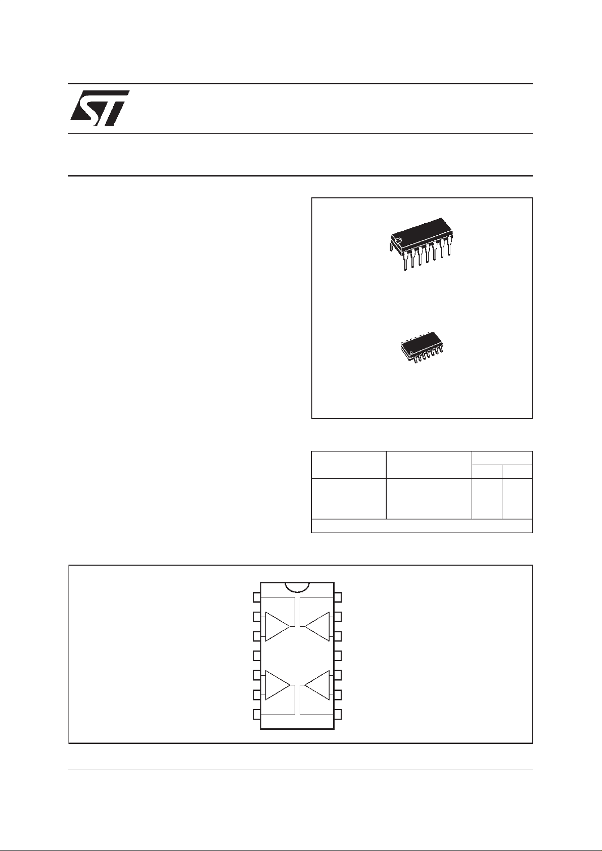
DIP14
(PlasticPackage)
D
SO14
(PlasticMicropackage)
DESC RIP TI ON
The TL074,T L074Aand TL074Bar ehi ghspeed
J–FETinputquadoper ati onalampli fi ersinc or porating
wellm atc hed,highv oltageJ–F ETand bipolartransistorsinamonolithicintegratedcircuit.
Thedev i c esfeaturehighslewrates,lowinputbiasand
offsetcurrents,andlow offsetvol t agetemperature
coefficient.
PIN CONNECTI O NS (topview)
Output 1
Inverting Input 1
Non-inverting Input 1
Non-inverting Input 2
Inverting Input 2
Output 2
1
2
-
+
3
+
4
V
CC
5
+
-
6
7
ORDER CODES
Part Number
TL074M/AM/BM –55
TL074I/AI/BI –40
TL074C/AC/BC 0
Example : TL074IN
14
Output 4
13
-
+
+
-
Inverting Input 4
12
Non-inverting Input 4
11
10
9
8
-
V
CC
Non-inverting Input 3
Inverting Input 3
Output 3
Temperature
Range
o
C, +125oC ••
o
C, +105oC ••
o
C, +70oC ••
Package
ND
December 1998
1/10
Page 2
TL074 - TL074A - TL074B
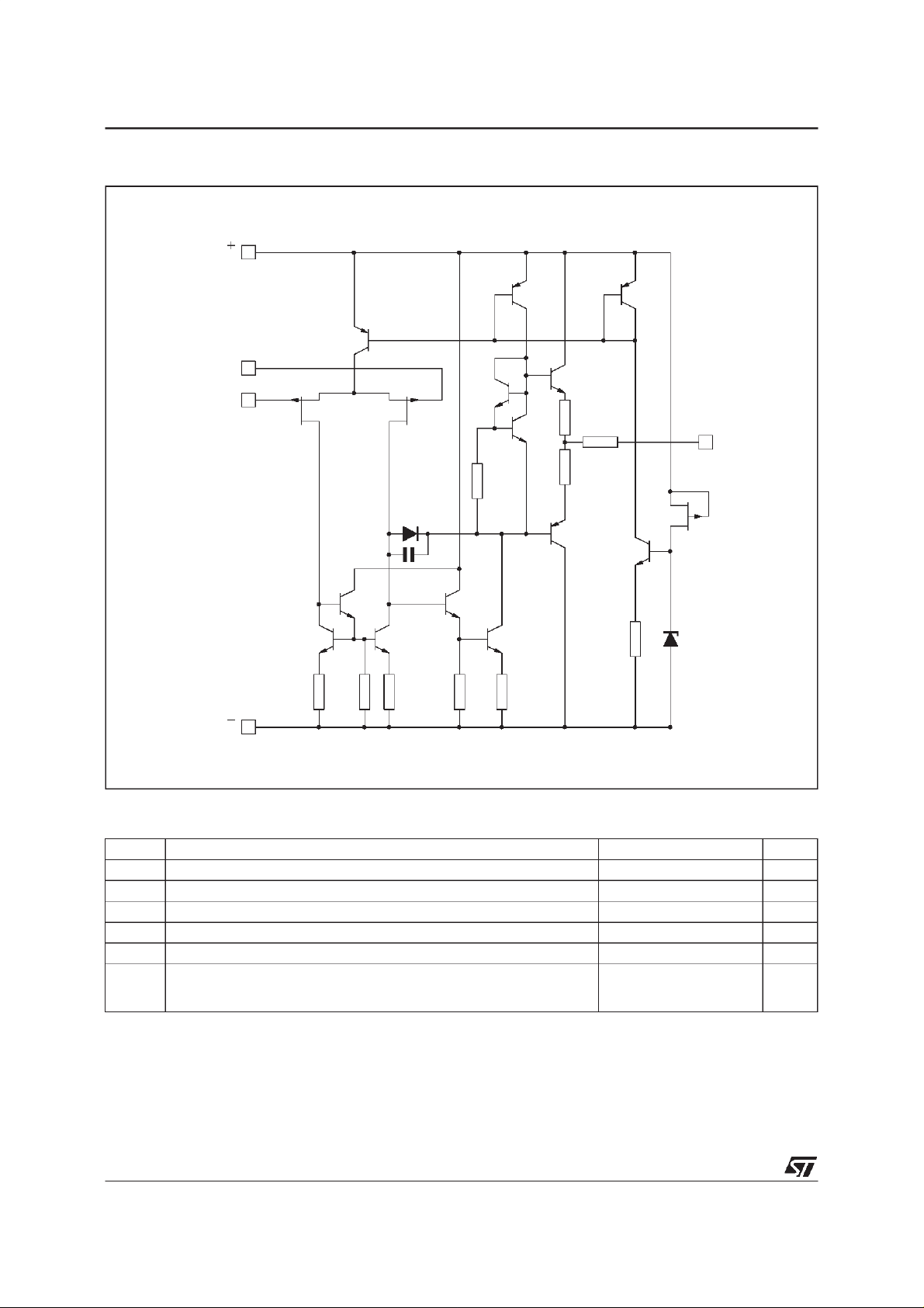
SCHEMATI C DIAGRAM
V
CC
Non -inverting
inp ut
Inverting
input
V
CC
1.3k
35k
1.3k
35k
30k
10 0
100
Ω10 0
Ω
Ω
200
8.2k
Ω
Output
1/4 TL074
ABSOLUTE MAXIMUM RATINGS
Symbol Parameter Value Unit
V
T
Notes : 1. All voltage values,exceptdifferentialvoltage, are withrespect to the zero reference level (ground) ofthe supplyvoltages where the
2/10
Supply Voltage - (note 1) ±18 V
CC
Input Voltage - (note 3) ±15 V
V
i
Differential Input Voltage - (note 2) ±30 V
V
id
Power Dissipation 680 mW
P
tot
Output Short-circuit Duration - (note 4) Infinite
Operating Free Air Temperature Range TL074C,AC,BC
oper
TL074I,AI,BI
TL074M,AM,BM
zero referencelevel isthe midpointbetween V
2. Differentialvoltages are atthe non-inverting inputterminal withrespect tothe invertinginput terminal.
3. The magnitude of theinput voltage mustneverexceed the magnitude of the supply voltage or 15 volts, whichever is less.
4. The outputmay be shorted to ground or toeither supply. Temperature and /orsupply voltages mustbe limited toensure thatthe
dissipation ratingis notexceeded.
+
CC
andV
–
.
CC
0to70
–40 to 105
–55 to 125
o
C
Page 3

TL074 - TL074A - TL074B
ELECTRICAL CHARACTERISTICS
= ±15V, T
V
CC
Symbol Parameter
V
DV
A
Input Offset Voltage (RS=50Ω)
io
Input Offset Voltage Drift 10 10 µV/oC
io
Input Offset Current *
I
io
Input Bias Current *
I
ib
Large Signal Voltage Gain (RL=2kΩ,VO=±10V)
vd
SVR Supply Voltage Rejection Ratio (R
I
V
Supply Current, per Amp, no Load
CC
Input Common Mode Voltage Range ±11 +15
icm
CMR Common Mode Rejection Ratio (R
Ios Output Short-circuit Current
±V
Output Voltage Swing
OPP
SR Slew Rate (V
T
amb
t
Rise Time (Vin= 20mV, RL=2kΩ,CL= 100pF,
r
T
amb
K
Overshoot (Vin= 20mV, RL=2kΩ,CL= 100pF,
OV
T
amb
GBP Gain Bandwidth Product (f = 100kHz,
T
amb
R
Input Resistance 10
i
THD Total Harmonic Distortion (f = 1kHz, A
R
L
Equivalent Input Noise Voltage
e
n
(f = 1kHz, R
∅m Phase Margin 45 45 Degrees
V
O1/VO2
* The inputbias currents arejunction leakage currents whichapproximately double for every 10oC increasein the junctiontemperature.
Channel Separation (Av= 100) 120 120 dB
=25oC (unless otherwise specified)
amb
TL074I,M,AC,AI,
AM,BC,BI,BM
Min. Typ. Max. Min. Typ. Max.
=25oC TL074
T
T
T
T
T
T
T
T
T
T
T
T
amb
min.
amb
min.
amb
min.
amb
min.
amb
min.
amb
min.
≤ T
amb
=25oC
≤ T
amb
=25oC
≤ T
amb
=25oC
≤ T
amb
=25oC
≤ T
amb
=25oC
≤ T
amb
≤ T
≤ T
≤ T
≤ T
≤ T
≤ T
max.
max.
max.
max.
max.
max.
TL074A
TL074B
TL074
TL074A
TL074B
=50Ω)
S
5025200 2515200
808086 707086
3
10
3
1
13
5 100
20 200
20
1.4 2.5
2.5
6
3
7
5
4
±11 +15
-12
=50Ω)
=25oC
T
amb
≤ T
T
min.
T
amb
T
min.
T
amb
T
min.
=25oC, unity gain) 8 13 8 13
≤ T
amb
max.
=25oC
≤ T
≤ T
amb
max.
=25oCR
≤ T
≤ T
amb
max.
= 10V, RL=2kΩ, CL= 100pF,
in
S
=2kΩ
L
= 10kΩ
R
L
RL=2kΩ
= 10kΩ
R
L
808086 707086
101040 6060101040 60
10
12
10
12
12
13.5
10
12
10
12
=25oC, unity gain) 0.1 0.1
=25oC, unity gain) 10 10
=25oC, Vin= 10mV, RL=2kΩ,CL= 100pF) 2 3 2 3
12
= 20dB,
=2kΩ,CL= 100pF, T
= 100Ω)
s
=25oC, VO=2VPP) 0.01 0.01
amb
V
15 15
TL074C
310
5 100
30 200
1.4 2.5
-12
12
13.5
12
10
13
10
20
2.5
60
Unit
mV
pA
nA
pA
nA
V/mV
dB
mA
V
dB
mA
V
V/µs
µs
%
MHz
Ω
%
nV
√Hz
3/10
Page 4

TL074 - TL074A - TL074B
MAXIMUM PEAK-TO-PEAK OUTPUT
VOLTAGE VERSUS FREQUENCY
VOLTAGE(V)
MAXIMUM PEAK-TO-PEAKOUTPUT
30
25
20
15
10
5
0
100 1K 10K 100K 10M1M
=
15VV
CC
=
10VV
CC
=5VV
CC
FREQUENCY (Hz)
R
L
T
amb
SeeFigure2
MAXIMUM PEAK-TO-PEAK OUTPUT
VOLTAGE VERSUS FREQUENCY
30
T
VOLTAGE (V)
MAXIMUMPEAK-TO-PEAK OUTPUT
=+25 C
amb
25
20
15
T
10
5
T
= +125 C
amb
0
10k 40k 100k 400k 1M 4M 10M
FREQUENCY (Hz)
V
CC
R
L
Se e Figure 2
=-55 C
amb
= 15V
=2k
=2kΩ
=+25°C
Ω
MAXIMUM PEAK-TO-PEAK OUTPUT
VOLTAGE VERSUS FREQUENCY
VOLTAGE (V)
MAXIMUMPEAK-TO-PEAK OUTPUT
30
25
20
V
CC
VCC=
15V
=
10V
15
10
VCC=
5
0
100 1K 10 K 100K 10M1M
FREQUENCY(Hz)
5V
= 10k
R
L
T
amb
See Figure 2
MAXIMUM PEAK-TO-PEAK OUTPUT
VOLTAGE VERSUS FREE AIR TEMP.
30
25
VOLTAGE (V)
MAXIMUM PEAK-TO-PEAKOUTPUT
20
15
10
V
5
0
=15V
CC
See Figure 2
-75 -25 25 7 5 125-50 0 50 -50
TEMPERATURE (°C)
R
R
= 10kΩ
L
=2kΩ
L
Ω
=+25 C
MAXIMUM PEAK-TO-PEAK OUTPUT
VOLTAGE VERSUS LOAD RESISTANCE
30
=
15VV
CC
VOLTAGE (V)
MAXIMUM PEAK-TO-PEAKOUTPUT
4/10
25
20
15
10
5
0
0.1 0.2 0.4 0.7 1 2 4 7 10
= +25°CT
amb
See Figure 2
LOAD R ESISTANCE (k
Ω)
MAXIMUM PEAK-TO-PEAK OUTP UT
VOLTAGE V ERSUS SUPPLY VOLTAGE
30
=10kΩ
R
L
25
T
= +25°C
amb
20
15
10
VOLTAGE (V)
5
02468101214 16
MAXIMUM PEAK-TO-PEAKOUTPUT
SUPPLY VOLTAGE ( V)
Page 5

TL074 - TL074A - TL074B
INPUT BIAS CURRENT VE RS US
FREE AIR TEMPERATURE
100
INPUTBIAS CURRENT(nA)
V
10
1
0.1
0.01
-50 -25 0 25 50 75 100 125
15V
=
CC
TEMPERATURE(°C)
LARGE SIG NAL DIFFERE NTIAL
VOLTAGE AMPLIFICATION AND PHASE
SHIFT VERSUS FREQUENCY
100
10
1
AMPLIFICATION(V/V)
DIFFERENTIAL VOLTAGE
100
PHASE SHIFT
(right scale)
R=2kΩ
L
C = 100pF
L
V=15V
CC
amb
T=+125
C
1K 10K 100K 10M1M
FREQUENCY(Hz)
DIFFERENTIAL
VOLTAGE
AMPLIFICATION
(left scale)
180
90
LARGE SI GNAL DIFFERE NT IAL
VOL TAGE AMPLIFI CAT I ON VE RSUS
FREE AIR TEMPERAT URE
1000
400
200
100
40
20
V
= 15V
CC
10
V
= 10V
O
4
AMPLIFICATION(V/V)
DIFFERENTIAL VOLTAGE
RL=2kΩ
2
1
-75 -50 -25 0 25 50 75
TEMPERATURE(°C)
100
125
TOTAL POWER DISSIPATION VERSUS
FREE AIR TEMPERATUR E
250
225
200
175
150
125
100
75
0
TOTAL POWERDISSIPATION (mW)
50
25
0
-75 -50 -25 0
25
TEMPERATURE (°C)
V
15V
=
CC
No signal
No load
50 75 100 125
SUPPLY CURRENT PER AMPLIFI ER
VERSUS FREE AIR TE MPE RATURE
2.0
V
CC
No signal
No load
50 75 100 125
SUPPLY CURRENT (mA)
1.8
1.6
1.4
1.2
1.0
0.8
0.6
0.4
0.2
0
-75 -50 -25 0
25
TEMPERATURE(°C)
COMMON MODE REJECTION RATIO
VERSUS FREE A IR TEMPERATURE
RATIO (dB)
89
R
=10kΩ
L
88
V
=15V
CC
87
86
85
84
83
-50 -25 0 25 50 75 100 125
-75
TEMPERATURE (°C)
5/10
15V
=
COMMON MODEMODEREJECTION
Page 6

TL074 - TL074A - TL074B
VOLTAGE FOLLOWER LARGE SIGNAL
PULSE RESPONSE
6
4
OUTPUT
INPUT
2
0
(V)
-2
-4
-6
INPUT AND OUTPUT VOLTAGES
V
=15V
CC
=2k
R
Ω
L
= 100pFC
L
T
=+25 C
amb
00.511.522.533.5
TIME (µs)
EQUIVALENT INPUT NOISE VOLTAGE
VERSUS FREQ UENCY
70
= 15V
V
CC
A
R
T
V
S
amb
=10
= 100 Ω
= +25°C
VOLTAGE (nV/VHz)
EQUIVALENTINPUT NOISE
60
50
40
30
20
10
0
10 40 100 400 1k 4k 10k 40k 100k
FREQUENCY (Hz)
OUTPUT VOLTAGE VERSUS
ELAPSED TIME
28
24
OVERSHOOT
20
90%
16
12
OUTPUT VOLTAGE(mV)
8
4
0
-4
10%
0 0.1 0.2
t
r
0.3
0.4
V
= 15V
CC
R
=2k
Ω
L
T
= +25°C
amb
0.5
0.6 0.7
TIME( µs)
TOTAL HARMONIC DISTORTION VERSUS
FREQUENCY
1
V
= 15V
V
= 15V
CC
0.4
0.1
0.04
(%)
0.01
0.004
0.001
TOTAL HARMONIC DISTORTION
CC
=1
=1
A
V
V
A
V
=6V
V
=6V
(rms)
O
(rms)
O
T
= +25°C
T
= +25°C
amb
amb
100 400 1k 4k 10k 40k 100k
FREQUENCY (Hz)
6/10
Page 7

PARAME TE R MEASUREMENT INFORMATION
TL074 - TL074A - TL074B
Figure 1 : Volt age Follower
-
1/4
TL074
e
I
CL= 100pF
R=2k Ω
L
TYP ICAL APP LIC ATI ONS
AUDI O DISTRIBUTIO N AMPL IFIER
e
o
f = 100kHz
O
Figur e 2 : Gain-o f-10 Inverting A mp lif ier
10k Ω
1k Ω
e
I
-
1/4
TL074
e
o
R
L
CL= 100pF
Input
1µF
100k
Ω 100k Ω
1OOµF
1M
Ω
-
1/4
TL074
100k Ω
100k
Ω
-
1/4
TL074
Output A
-
1/4
TL074
+
V
CC
Output B
-
1/4
TL074
Output C
7/10
Page 8

TL074 - TL074A - TL074B
TYP ICAL APP LIC ATI ONS (continued)
POSITIVE FEEDBACK BAN DPASS FILTER
Input
43k Ω
1.5k
OUTPUT A
16k Ω
220p F
43k Ω
Ω
43k Ω
220p F
1.5k Ω
OutputA
-
1/4
TL074
30k
-
220pF
Ω
1/4
TL074
43k Ω
-
1/4
TL0 74
220pF
43k Ω
16k Ω
43k Ω
-
1/4
TL074
30k Ω
Output B
Ground
OUTPUT B
SECOND ORDER BANDPASS F ILTER
fo = 100kHz ; Q = 30 ; Gain = 16
8/10
CASCAD E D BAND P AS S FILT ER
fo=100kHz;Q=69;Gain=16
Page 9

PACKAG E MECHANICAL DATA
14 PINS - PLASTI C DIP
TL074 - TL074A - TL074B
Dimensions
a1 0.51 0.020
B 1.39 1.65 0.055 0.065
b 0.5 0.020
b1 0.25 0.010
D 20 0.787
E 8.5 0.335
e 2.54 0.100
e3 15.24 0.600
F 7.1 0.280
i 5.1 0.201
L 3.3 0.130
Z 1.27 2.54 0.050 0.100
Min. Typ. Max. Min. Typ. Max.
Millimeters Inches
9/10
Page 10

TL074 - TL074A - TL074B
PACKAG E MECHANICAL DATA
14 P INS - PLASTIC MICROPACKAGE (SO)
Dimensions
Min. Typ. Max. Min. Typ. Max.
Millimeters Inches
A 1.75 0.069
a1 0.1 0.2 0.004 0.008
a2 1.6 0.063
b 0.35 0.46 0.014 0.018
b1 0.19 0.25 0.007 0.010
C 0.5 0.020
c1 45
o
(typ.)
D 8.55 8.75 0.336 0.334
E 5.8 6.2 0.228 0.244
e 1.27 0.050
e3 7.62 0.300
F 3.8 4.0 0.150 0.157
G 4.6 5.3 0.181 0.208
L 0.5 1.27 0.020 0.050
M 0.68 0.027
S8
Information furnished is believed to be accurate and reliable. However, STMicroelectronics assumes no responsibility for the
consequences of use of such information nor for any infringement of patents or other rights of third parties which may result
from its use. No license is granted by implication or otherwise under any patent or patent rights of STMicroelectronics. Specifications mentioned in this publication are subject to change without notice. This publication supersedes and replaces all information previously supplied. STMicroelectronics products are not authorized for use as critical components in life support
devices or systems without express written approval of STMicroelectronics.
The ST logo is a trademark of STMicroelectronics
1998 STMicroelectronics – Printed in Italy – All Rights Reserved
STMicroelectronics GROUP OF COMPANIES
Australia - Brazil - Canada - China - France - Germany - Italy - Japan - Korea - Malaysia - Malta - Mexico - Morocco
The Netherlands - Singapore - Spain - Sweden - Switzerland - Taiwan - Thailand - UnitedKingdom - U.S.A.
http://www.st.com
o
(max.)
10/10
 Loading...