

Page 1
UNISONIC TECHNOLOGIES CO., LTD
TL072
LINEAR INTEGRATED CIRCUIT
LOW NOISE DUAL J-FET
OPERATIONAL AMPLIFIER
DESCRIPTION
The UTC TL072 is a high speed J-FET input quad operational
amplifier. It incorporates well matched, high voltage J-FET and
bipolar transistors in a monolithic integrated circuit. The device
features high slew rates, low input bias and offset current, and low
offset voltage temperature coefficient.
FEATURES
*Low power consumption
*Wide common-mode (up to V
*Low input bias and offset current
*Low noise en = 15nV /
*Output short-circuit protection
*High input impedance J-FET input stage
*Low harmonic distortion:0.01%(typ)
*Internal frequency compensation
*Latch up free operation
*High slewrate:16V/s(typ)
) and differential voltage range
CC+
Hz
(typ)
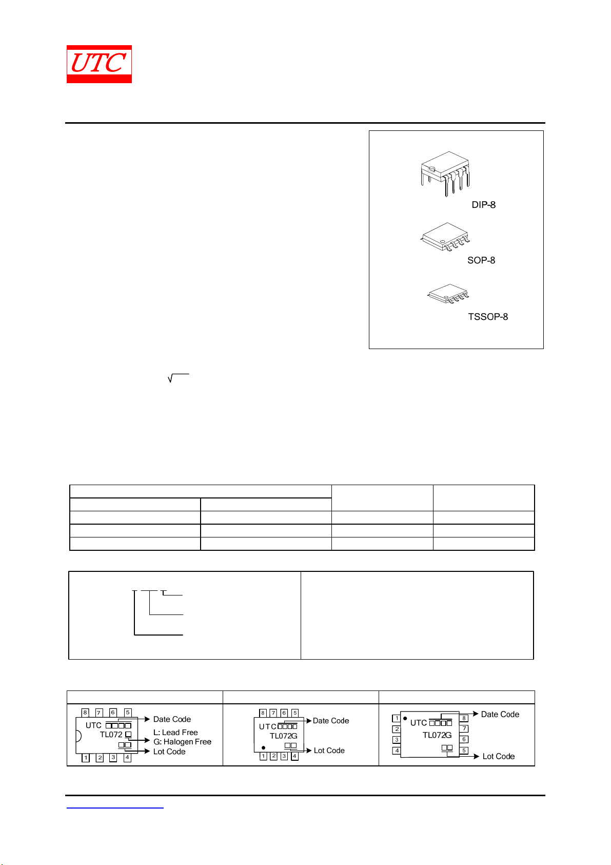
ORDERING INFORMATION
Ordering Number
Lead Free Halogen Free
TL072L-D08-T TL072G-D08-T DIP-8 Tube
- TL072G-S08-R SOP-8 Tape Reel
- TL072G-P08-R TSSOP-8 Tape Reel
TL072L-D08-T
(1)Packing Type
(2)Package Type
(3)Green Package
MARKING
DIP-8 SOP-8 TSSOP-8
Package Packing
(1) T: Tube, R: Tape Reel
(2) D08: DIP-8, S08: SOP-8, P08: TSSOP-8
(3) L: Lead Free, G: Halogen Free and Lead Free
www.unisonic.com.tw 1 of 8
Copyright © 2015 Unisonic Technologies Co., Ltd QW-R105-004.G
Page 2
TL072 LINEAR INTEGRATED CIRCUIT
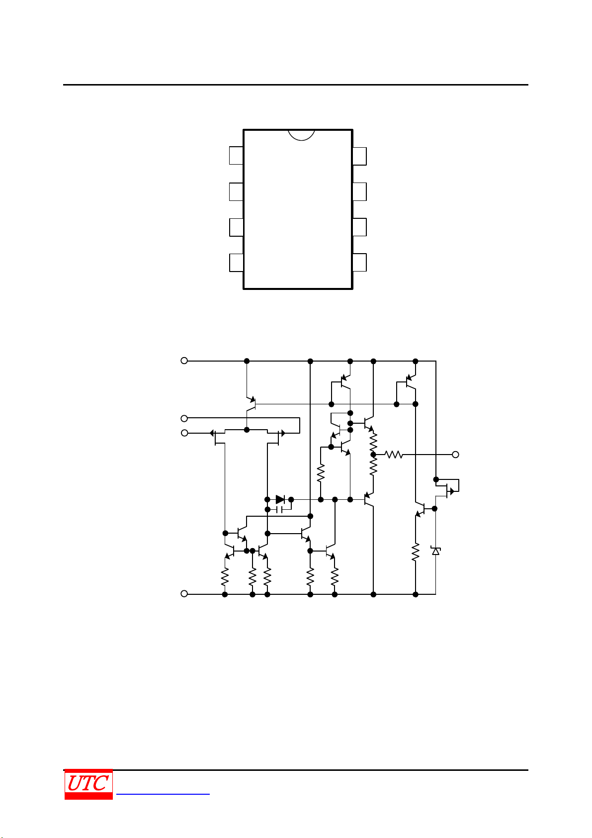
PIN CONFIGURATION
OUTPUT 1
INVERTING INPUT 1
NON-INVERTING INPUT 1
BLOCK DIAGRAM
V
CC+
Non-inverting input
Inverting input
Vcc-
1
2
3
4
30k
8
Vcc+
OUTPUT 2
7
INVERTING INPUT 2
6
NON-INVERTING INPUT 2
5
100Ω
100Ω
200Ω
Output
8.2k
1.3k
V
CC-
35k
1.3k
35k
100Ω
UNISONIC TECHNOLOGIES CO., LTD 2 of 8
www.unisonic.com.tw QW-R105-004.G
Page 3

TL072 LINEAR INTEGRATED CIRCUIT
ABSOLUTE MAXIMUM RATINGS (T
=25C, unless otherwise specified)
A
PARAMETER SYMBOL RATINGS UNIT
Supply Voltage (note 1) VCC ±18 V
Input Voltage (note 2) VIN ±15 V
Differential Input Voltage (note 3) V
±30 V
I(DIFF)
Power Dissipation PD 680 mW
Output Short-Circuit Duration (Note 4) Infinite
Operating Temperature T
Storage Temperature T
0 ~ +70 C
OPR
-65 ~ +150 C
STG
Notes: 1. All voltage values, except differential voltage, are with respect to the zero reference level (ground) of the
supply voltages where the zero reference level is the midpoint between V
- and VCC+.
CC
2. The magnitude of the input voltage must never exceed the magnitude of the supply voltage or 15 volts,
whichever is less.
3. Differential voltages are at the non-inverting input terminal with respect to the inverting input terminal.
4. The output may be shorted to ground or to either supply. Temperature and/or supply voltages must be
limited to ensure that the dissipation rating is not exceeded.
5. Absolute maximum ratings are those values beyond which the device could be permanently damaged.
Absolute maximum ratings are stress ratings only and functional device operation is not implied.
UNISONIC TECHNOLOGIES CO., LTD 3 of 8
www.unisonic.com.tw QW-R105-004.G
Page 4
TL072 LINEAR INTEGRATED CIRCUIT
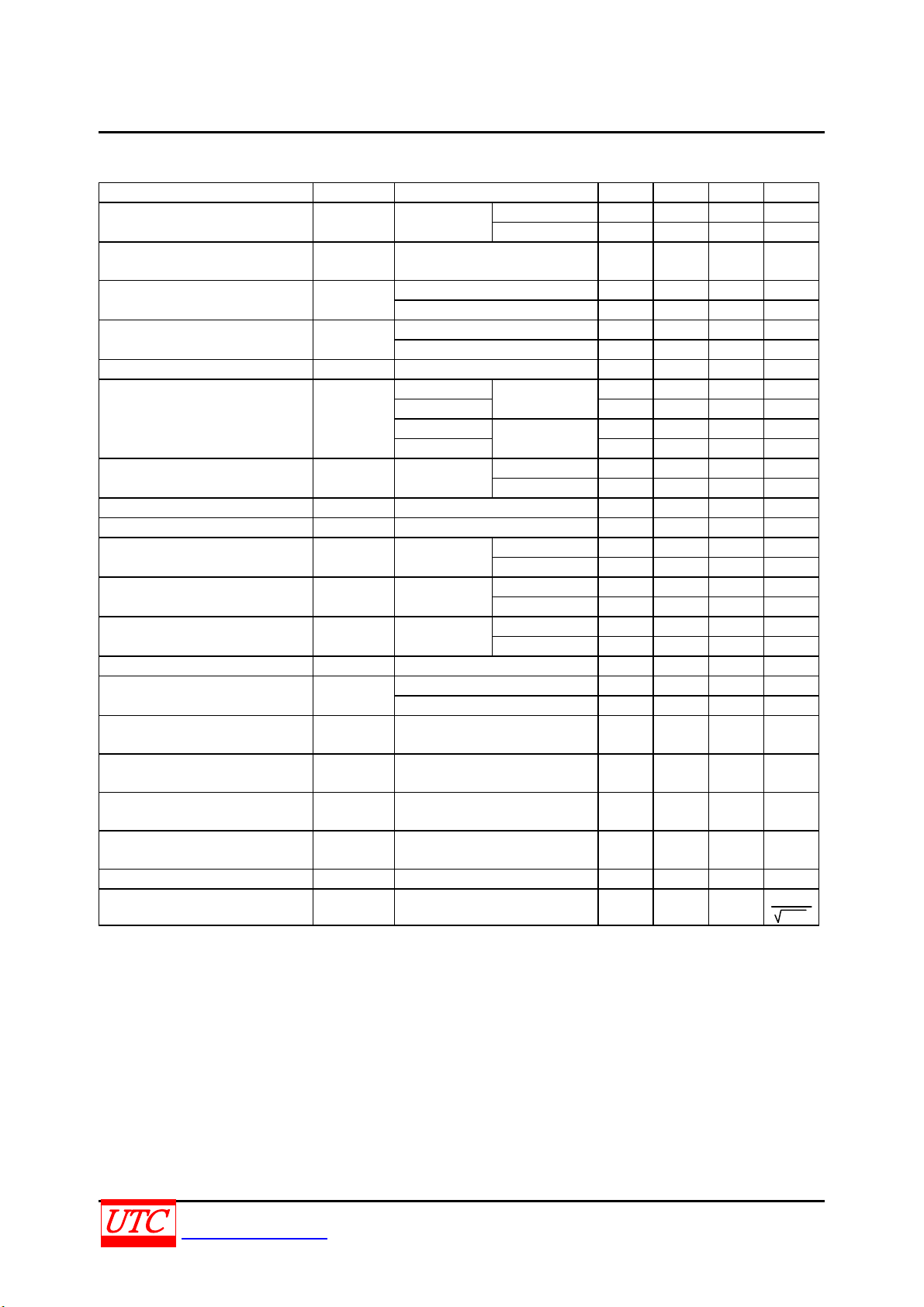
ELECTRICAL CHARACTERISTICS
(VCC=±15V, Ta=25C, T
PARAMETER SYMBOL CONDITIONS MIN TYP MAX UNIT
Input Offset Voltage V
Temperature Coefficient of Input
Offset Voltage
Input Offset Current* I
Input Bias Current* I
Input Common Mode Voltage V
Output Voltage Swing V
Large Signal Voltage Gain Avd
Gain Bandwidth Product GBW TA=25C, RL=10k, CL=100pF 2.5 4 MHz
Input Resistance RIN 1012
Common Mode Rejection Ratio CMR RS=50
Supply Voltage Rejection Ratio SVR RS=50
Supply Current ICC No load
Channel Separation V01/V02 GV=100 120 dB
Output Short-circuit Current Ios
Slew Rate SR
Rise Time tR
Overshoot Factor Kov
Total Harmonic Distortion THD
Phase Margin m 45
Equivalent Input Noise Voltage eN RS=100, f=1KHz 15
*The Input bias currents are junction leakage currents, which approximately double for every 10C increase in the
junction temperature.
=0C, T
MIN
=70C, unless otherwise specified)
MAX
RS=50
I(OFF)
∆V
RS=50 10 μV/C
I(OFF)
TA=25C 5 100 pA
I(OFF)
I(BIAS)
I(CM)
T
MIN≦TA≦TMAX
TA=25C 20 200 pA
T
MIN≦TA≦TMAX
±11
RL=2k 10 12 V
RL=10k
O(SW)
RL=2k 10 V
R
=10k
L
R
=10k,
L
V
=±10V
OUT
TA=25C 3 10 mV
T
T
T
TA=25C 25 200 V/mV
T
TA=25C 70 86 dB
T
TA=25C 70 86 dB
T
TA=25C 1.4 2.5 mA
T
TA=25C 10 40 60 mA
T
MIN≦TA≦TMAX
V
=10V, RL=2k, CL=100pF,
IN
unity gain
V
=20mV, RL=2k, CL=100pF,
IN
unity gain
V
=20mV,RL=2k,CL=100pF,
IN
unity gain
G
=20dB, f=1kHz, RL=2k,
V
C
=100pF, V
L
OUT
=2Vpp
MIN≦TA≦TMAX
=25C
A
MIN≦TA≦TMAX
MIN≦TA≦TMAX
MIN≦TA≦TMAX
MIN≦TA≦MAX
MIN≦TA≦TMAX
13 mV
10 nA
20 nA
-12~+15
V
12 13.5 V
12 V
15 V/mV
70 dB
70 dB
2.5 mA
10 60 mA
8 16 V/μs
0.1 μs
10 %
0.01 %
Degrees
nV
Hz
UNISONIC TECHNOLOGIES CO., LTD 4 of 8
www.unisonic.com.tw QW-R105-004.G
Page 5
TL072 LINEAR INTEGRATED CIRCUIT
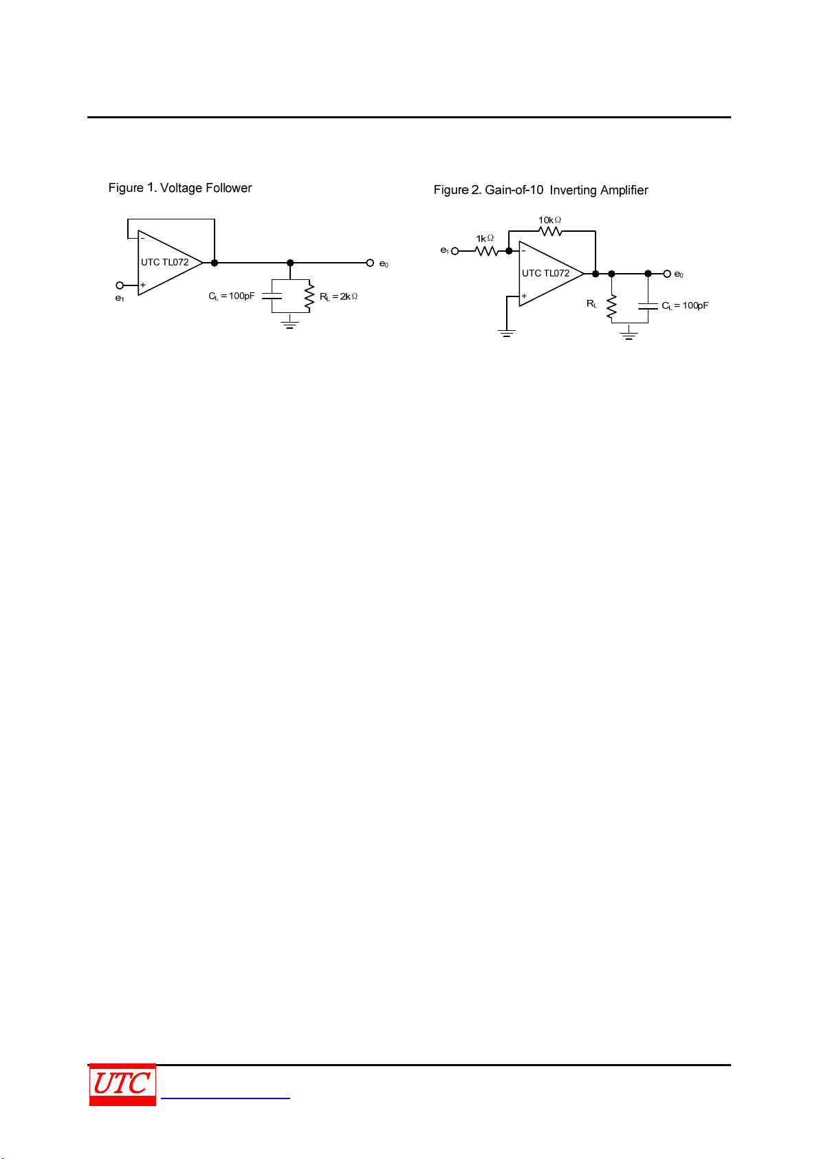
PARAMETER MEASUREMENT INFORMATION
UNISONIC TECHNOLOGIES CO., LTD 5 of 8
www.unisonic.com.tw QW-R105-004.G
Page 6
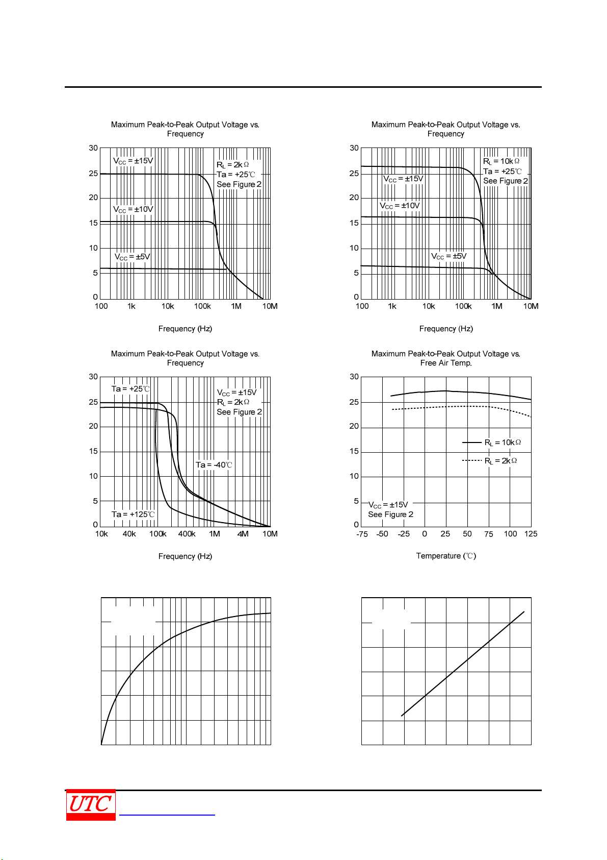
TL072 LINEAR INTEGRATED CIRCUIT
TYPICAL CHARACTERISTICS
Mzximum Peak-to-Peak Output Voltage (V)
Mzximum Peak-to-Peak Output Voltage (V)
Mzximum Peak-to-Peak Output Voltage (V)
Mzximum Peak-to-Peak Output Voltage (V)
Maximum Peak-to-Peak Output Voltage vs.
30
VCC= ±15V
Ta = +25℃
25
See Figure 2
20
Load Resistance
Maximum Peak-to-Peak Output Voltage vs.
30
RL= 10kΩ
25
Ta = +25℃
20
Supply Voltage
15
(V)
10
5
Mzximum Peak-to-Peak Output Voltage
0
0.1
0.40.2
Load Resistance (kΩ)
1
4
7841420.7
10
15
(V)
10
5
Mzximum Peak-to-Peak Output Voltage
0
0
6
Supply Voltage (±V)
12
102
16
UNISONIC TECHNOLOGIES CO., LTD 6 of 8
www.unisonic.com.tw QW-R105-004.G
Page 7
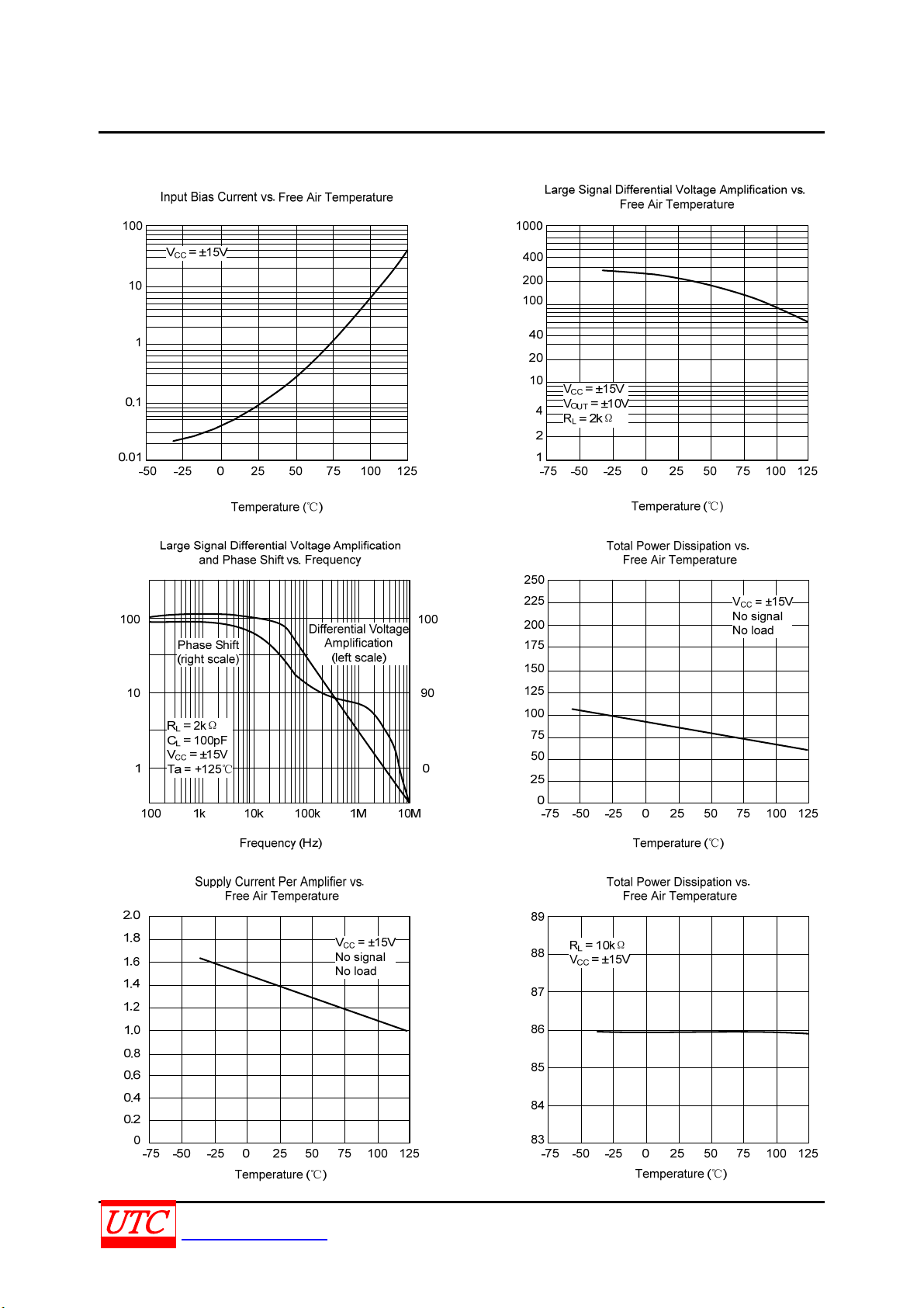
TL072 LINEAR INTEGRATED CIRCUIT
TYPICAL CHARACTERISTICS(Cont.)
Input Bias Current (nA)
Differential Voltage Amplification (V/V)
Total Power Dissipation (mW)
Differential Voltage Amplification (V/V)
Supply Current (mA)
Common Mode Rejection Ratio (dB)
UNISONIC TECHNOLOGIES CO., LTD 7 of 8
www.unisonic.com.tw QW-R105-004.G
Page 8
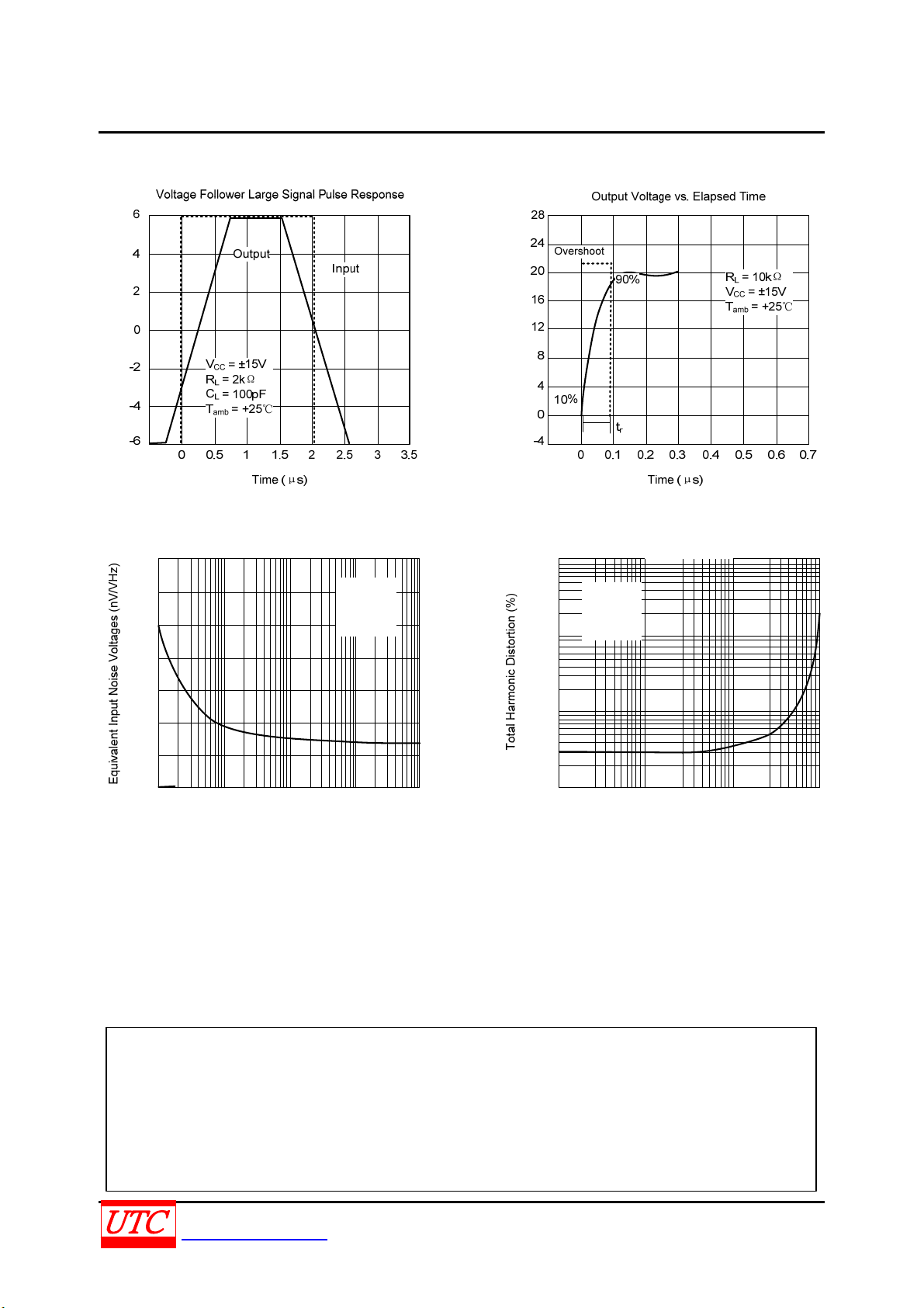
TL072 LINEAR INTEGRATED CIRCUIT
TYPICAL CHARACTERISTICS(Cont.)
Output Voltage (mV)
Input and Output Voltages (V)
70
60
50
40
30
20
10
Equivalent Input Noise Voltage vs.
Frequency
VCC= ±15V
A
= 10
V
= 100Ω
R
S
Ta = +25℃
1
0.4
0.1
0.04
0.01
0.004
Total Harmonic Distortion vs.
VCC= ±15V
A
= 1
V
V
= 6V
O(ms)
Ta = +25℃
Frequency
0
10
40
Frequency (Hz)
10k 4k 40k4k400
100k
40k1k100
0.001
400
1k
Frequency (Hz)
10k100
UTC assumes no responsibility for equipment failures that result from using products at values that
exceed, even momentarily, rated values (such as maximum ratings, operating condition ranges, or
other parameters) listed in products specifications of any and all UTC products described or contained
herein. UTC products are not designed for use in life support appliances, devices or systems where
malfunction of these products can be reasonably expected to result in personal injury. Reproduction in
whole or in part is prohibited without the prior written consent of the copyright owner. The information
presented in this document does not form part of any quotation or contract, is believed to be accurate
and reliable and may be changed without notice.
UNISONIC TECHNOLOGIES CO., LTD 8 of 8
www.unisonic.com.tw QW-R105-004.G
100k
 Loading...