

Datasheet TL064ID, TL064I, TL064M, TL064IN, TL064ACD Datasheet (SGS Thomson Microelectronics)
...Page 1
LOW POWER J-FET QUAD OPERATIONAL AMPLIFIERS
■
VERYLOWPOWER CONSUMPTION : 200µA
■
WIDE COMMON-MODE (UP TO V
DIFFERENTIALVOLTAGERANGES
■
LOW INPUTBIAS AND OFFSETCURRENTS
■
OUTPUTSHORT-CIRCUIT PROTECTION
■
HIGH INPUT IMPEDANCE J-FET INPUT
STAGE
■
INTERNAL FREQUENCYCOMPENSATION
■
LATCHUP FREE OPERATION
■
HIGH SLEW RATE: 3.5V/µs
CC
+
) AND
TL064
TL064A - TL064B
DESCRIPTION
The TL064, TL064Aand TL064B are high speed
J-FET input quad operational amplifiers. Each of
these J-FET input operational amplifiers incorporateswellmatched, highvoltage J-FETand bipolar
transistorsin a monolithicintegrated circuit.
The device featureshigh slewrate, low input bias
and offsetcurrents,andlowoffsetvoltagetemperature coefficient.
PIN CONNECTIONS(top view)
Output 1
Inverting Input 1
Non-inverting Input 1
Non-inverting Input2
Inverting Input 2
Output 2
1
2
-
+
3
+
V
4
CC
5
+
-
6
7
N
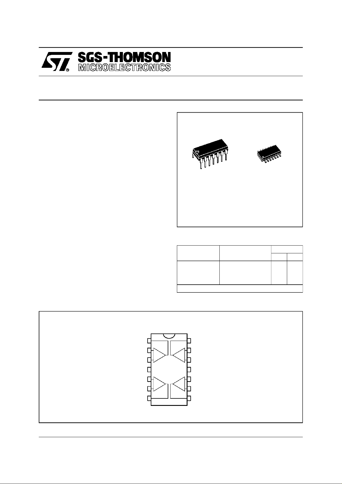
DIP14
(Plastic Package)
(Plastic Micropackage)
ORDER CODES
Part Number Temperature Range
o
TL064M/AM/BM -55
TL064I/AI/BI -40
TL064C/AC/BC 0
Example : TL064IN
14
Output 4
13
-
+
+
-
Inverting Input 4
12
Non-inverting Input 4
-
V
11
CC
10
Non-inverting Input 3
9
Inverting Input 3
8
Output 3
C, +125oC ••
o
C, +105oC ••
o
C, +70oC ••
D
SO14
Package
ND
October 1997
1/10
Page 2
TL064 - TL064A - TL064B
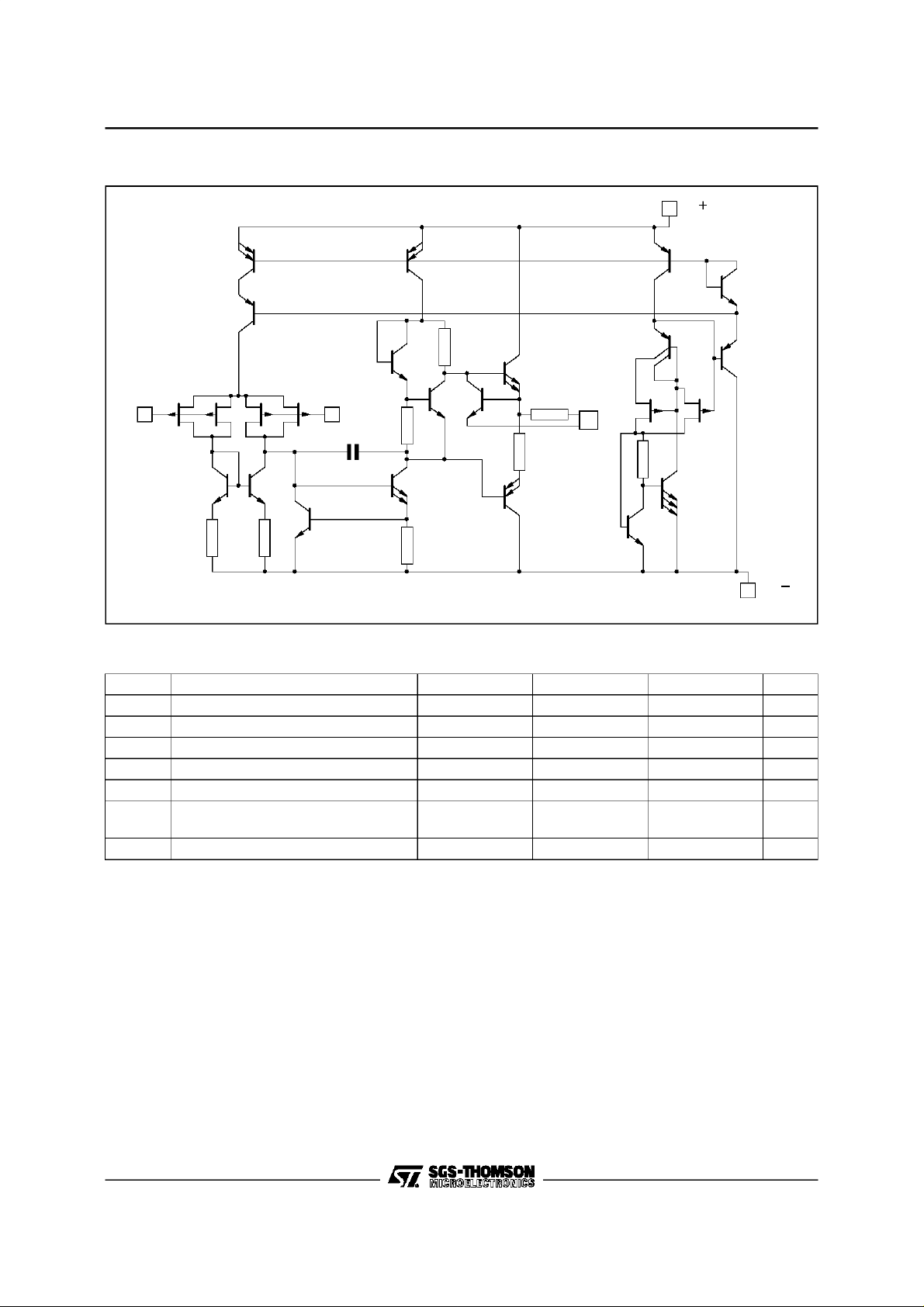
SCHEMATIC DIAGRAM
220Ω
V
CC
Inverting
Input
4.2k
Ω
Non-inverting
Input
45k
100Ω
Output
64
Ω
1/4 TL064
Ω
270Ω
3.2k
Ω
V
CC
MAXIMUMRATINGS
Symbol Parameter TL064M,AM,BM TL064I,AI,BI TL064C,AC,BC Unit
V
V
P
T
T
Notes : 1. All voltage values, except differential voltage,are withrespect to thezero reference level (ground) of the supply voltages where
Supply Voltage -(note 1) ±18 ±18 ±18 V
CC
Input Voltage - (note3) ±15 ±15 ±15 V
V
i
Differential Input Voltage - (note 2) ±30 ±30 ±30 V
id
Power Dissipation 680 680 680 mW
tot
Output Short-Circuit Duration (Note4) Infinite Infinite Infinite
Operating Free-Air Temperature
oper
-55 to +125 -40 to +105 0 to +70
Range
Storage Temperature Range -65 to +150 -65 to +150 -65 to +150
stg
the zero reference level is themidpoint between V
+
CC
2. Differential voltages are the non-inverting input terminal with respect to the inverting input terminal.
3. The magnitudeof the input voltage must never exceed the magnitudeof the supply voltage or 15 volts, whicheveris less.
4. The outputmay be shorted toground or to either supply. Temperature and/orsupply voltages must be limited to ensure that the
dissipation rating is notexceeded.
and V
-
.
CC
o
C
o
C
2/10
Page 3
TL064 - TL064A - TL064B
ELECTRICAL CHARACTERISTICS
=±15V,T
V
CC
Symbol Parameter
Input Offset Voltage(Rs=50Ω)
V
io
DV
Temperature Coefficient of Input
io
Offset Voltage (R
Input OffsetCurrent*
I
io
Input Bias Current*
I
ib
V
Input Common Mode Voltage
icm
Range
V
Output Voltage Swing (RL= 10kΩ)
OPP
A
Large Signal Voltage Gain
vd
(R
L
GBP Gain Bandwidth Product
(T
amb
C
= 100pF)
L
Input Resistance 10
R
i
CMR Common Mode Rejection Ratio
(R
s
SVR Supply Voltage Rejection Ratio
(R
s
Supply Current (Per Amplifier)
I
cc
(T
amb
V
O1/VO2
* The input bias currents ofa FET-input operational amplifier are normaljunction reverse currents, which are temperature sensitive.
Pulse techniques must be used thatwill maintain the junction temperatureas close to the ambient temperature as possible.
Channel Separation
(A
v
Total Power Consumption
P
D
(T
amb
=25oC (unless otherwise specified)
amb
=25oC
T
amb
T
. ≤ T
min
T
amb
. ≤ T
T
min
T
amb
T
min.
T
amb
T
. ≤ T
min
amb
=50Ω)
s
=25oC
amb
=25oC
≤ T
amb
=25oC
amb
≤ T
≤ T
≤ T
≤ T
max.
max.
max
max
.
.
= 10kΩ,Vo=±10V)
=25oC
T
amb
T
min
. ≤ T
amb
≤ T
max
.
=25oC, RL= 10kΩ
= 50Ω)
=50Ω)
=25oC, noload, no signal)
= 100,T
amb
=25oC)
=25oC, noload, no signal)
TL064M TL064I TL064C
Min. Typ. Max. Min. Typ. Max. Min. Typ. Max.
36
15
36
9
315
20
10 10 10
5 100
30 200
±11.5 +15
-12
20
50
±11.5 +15
5 100
10
30 200
20
-12
5 2005pA
30 40010pA
±11 +15
-12
202027 202027 202027
4
64
4
63
4
6
3
111
12
10
12
10
12
80 86 80 86 70 76
80 95 80 95 70 95
200 250 200 250 200 250
120 120 120
6 7.5 6 7.5 6 7.5
Unit
mV
µV/
nA
nA
V
V
V/mV
MHz
Ω
dB
dB
µA
dB
mW
o
C
ELECTRICAL CHARACTERISTICS (continued)
=±15V,T
V
CC
Symbol Parameter
SR Slew Rate (V
Rise Time (Vi= 20mV,RL= 10kΩ,CL= 100pF, AV= 1) (see Figure 1) 0.2 µs
t
r
K
Overshoot Factor (Vi= 20mV, RL= 10kΩ,CL= 100pF, AV=1)
OV
(see figure 1)
Equivalent Input Noise Voltage
e
n
(R
s
=25oC
amb
= 10V, RL= 10kΩ,CL= 100pF, AV= 1) 1.5 3.5 V/µs
i
= 100Ω, f = 1KHz)
TL064C,I,M
Min. Typ. Max.
10
42
Unit
%
nV
√Hz
3/10
Page 4

TL064 - TL064A - TL064B
ELECTRICAL CHARACTERISTICS (continued)
=±15V,T
V
CC
Symbol Parameter
Input Offset Voltage(Rs=50Ω)
V
io
DV
V
V
Temperature Coefficient of InputOffset Voltage
io
(R
s
Input OffsetCurrent*
I
io
Input Bias Current*
I
ib
Input Common Mode VoltageRange ±11.5 +15
icm
Output Voltage Swing (RL= 10kΩ)
OPP
A
Large Signal Voltage Gain (RL= 10kΩ,Vo=±10V)
vd
GBP Gain Bandwidth Product
(T
amb
Input Resistance 10
R
i
CMR Common Mode Rejection Ratio(R
SVR Supply Voltage Rejection Ratio (R
I
Supply Current (Per Amplifier)
cc
(T
amb
V
O1/VO2
Channel Separation
(A
v
Total Power Consumption(Each Amplifier)
P
D
(T
amb
SR Slew Rate (V
Rise Time (Vi= 20mV,RL= 10kΩ,CL= 100pF, AV= 1) 0.2 0.2 µs
t
r
K
* The input bias currents ofa FET-input operational amplifier are normaljunction reverse currents, which are temperature sensitive.
Pulse techniques must be used thatwill maintain the junction temperatureas close to the ambient temperature as possible.
Overshoot Factor (Vi= 20mV, RL= 10kΩ,CL= 100pF,
OV
A
= 1) - (see figure 1)
V
Equivalent Input Noise Voltage
e
n
(R
s
=25oC (unless otherwise specified)
amb
=25oC
T
amb
T
min
. ≤ T
amb
≤ T
max.
=50Ω)
T
=25oC
amb
. ≤ T
T
min
T
amb
. ≤ T
T
min
T
amb
T
. ≤ T
min
T
amb
T
. ≤ T
min
amb
=25oC
amb
=25oC
amb
=25oC
amb
≤ T
≤ T
≤ T
≤ T
max.
max.
max
max.
.
=25oC, RL= 10kΩ,CL= 100pF)
s
s
=25oC, noload, no signal)
= 100,T
amb
=25oC)
=25oC, noload, no signal)
= 10V, RL= 10kΩ,CL= 100pF, AV= 1) 1.5 3.5 1.5 3.5 V/µs
i
= 100Ω, f = 1KHz)
=50Ω)
=50Ω)
TL064AC,AI,AM TL064BC,BI,BM
Min. Typ. Max. Min. Typ. Max.
36
7.5
23
5
10 10
5 100
5 1003pA
3
30 200
30 2007pA
7
±11.5 +15
-12
-12
202027 202027
4
64
4
6
4
11
12
10
12
80 86 80 86
80 95 80 95
200 250 200 250
120 120
6 7.5 6 7.5
10 10
42 42
Unit
mV
µV/
nA
nA
V
V
V/mV
MHz
Ω
dB
dB
µA
dB
mW
%
nV
√Hz
o
C
4/10
Page 5

TL064 - TL064A - TL064B
MAXIMUM PEAK-TO-PEAK OUTPUT
VOLTAGE VERSUSSUPPLY VOLTAGE
30
R
=10kΩ
L
T
= +25°C
am b
See fig ure 2
5
0246810121416
SUPPLY VOLTAGE (V)
VOLTAGE(V)
MAXIMUM PEAK-TO-PEAKOUTPUT
25
20
15
10
MAXIMUM PEAK-TO-PEAK OUTPUT
VOLTAGEVERSUS LOAD RESISTANCE
30
25
20
15
VOLTAGE (V)
MAXIMUM PEAK-TO-PEAKOUTPUT
10
5
0
100 200 400 700
1k
2k 4k 7k 10k
= 15V
V
CC
T
= +25°C
amb
SeeFigure2
LOAD RESISTANCE(kΩ)
MAXIMUMPEAK-TO-PEAKOUTPUT
VOLTAGE VERSUSFREE AIR TEMP.
30
25
20
15
10
V
= 15V
VOLTAGE(V)
MAXIMUM PEAK-TO-PEAKOUTPUT
CC
R
= 10k Ω
L
5
See Figure 2
0
-75 -25 2 5 75 125-50 0 5 0 -50
FREE AIR TEMPERATURE (°C)
MAXIMUM PEAK-TO-PEAK OUTPUT
VOLTAGEVERSUS FREQUENCY
30
MAXIMUM PEAK-TO-PEAKOUTPUT
VOLTAGE (V)
25
20
15
10
5
0
1k
=
15VV
CC
=
12VV
CC
=
5VV
CC
= 2VV
CC
10K 100K 10M1M
FREQUENCY(Hz)
R
= 10kΩ
L
T
= +25°C
amb
See Figure2
DIFFERENTIALVOLTAGEAMPLIFICATION
VERSUS FREE AIR TEMPERATURE
10
7
4
2
V = 15V
1
-75
CC
R = 10kΩ
L
-25 0 25 50 75 100 125
-50
FREE AIR TEMPERATURE (°C)
DIFFERENTIAL VOLTAGE
AMPLIFICATION(V/mV)
LARGE SIGNALDIFFERENTIAL VOLTAGE
AMPLIFICATION AND PHASE SHIFTVERSUS
FREQUENCY
6
AMPLIFICATION (V/V)
DIFFERENTIAL VOLTAGE
10
10
10
10
10
10
5
4
3
2
PHASE SHIFT
1
(right scale)
10 100 1k 10k
1
V
= 5V to 15V
CC
=2kΩ
R
L
=+25°CT
amb
FREQUENCY (Hz)
DIFFERENTIAL
VOLTAGE
AMPLIFICATION
(left scale)
100k
1M
0
45
90
135
180
10M
5/10
Page 6

TL064 - TL064A - TL064B
SUPPLY CURRENT PER AMPLIFIER VERSUS
SUPPLY VOLTAGE
250
200
150
100
T
=+25°C
amb
50
SUPPLY CURRENT (µA)
Nosignal
No load
0
02
4
6
10 12 14
8
SUPPLY VOLTAGE ( V)
TOTALPOWERDISSIPATEDVERSUS
FREE AIR TEMPERATURE
30
25
20
16
SUPPLYCURRENT PER AMPLIFIER VERSUS
FREE AIR TEMPERATURE
250
200
150
100
V
= 15V
50
SUPPLY CURRENT(µA)
CC
No signal
Noload
0
-75 -50
-25
0
50 75 100
25
125
FREE AIR TEMPERATURE(°C)
COMMONMODEREJECTION RATIO
VERSUSFREE AIR TEMPERATURE
87
86
85
15
(mW)
10
5
TOTAL POWER DISSIPATED
=
CC
No signal
Noload
15VV
0
-50 -25 0255075100125
-75
FREE AIR TEMPERATURE(°C)
NORMALIZED UNITY GAIN BANDWIDTH
SLEW RATE,AND PHASE SHIFT VERSUS
TEMPERATURE
1.3
1.2
1.1
1
0.9
AND SLEW RATE
0.8
0.7
NORMALIZEDUNITY-GAINBANDWIDTH
-75
PHASE SHI FT
UNITY-GAIN-BANDWIDTH
(left scale)
V
15V
=
CC
R
= 10k
Ω
L
f = B forphase shift
1
-50 -25 0 25 50 75 100 125
FREE AIR TEMPERATURE(°C)
(right scale)
SLEW RATE
(left scale)
1.03
1.02
1.01
0.99
0.98
0.97
84
(dB)
83
15VV
=
CC
RL=10kΩ
COMMONMODEREJECTIONRATIO
82
81
-50 -25 0 25 50 75 100 125
-75
FREE AIR TEMPERATURE(°C)
INPUT BIAS CURRENT VERSUS FREE AIR
TEMPERATURE
100
NORMALIZEDPHASESHIFT
V
10
1
1
0.1
INPUT BIAS CURRENT (nA)
0.01
-50 -25 0 255075100125
15V
=
CC
FREEAIR TEMPERATURE (°C)
6/10
Page 7

TL064 - TL064A - TL064B
VOLTAGEFOLLOWER LARGE SIGNAL
RESPONSE
6
4
2
0
(V)
-2
-4
INPUT AND OUTPUT VOLTAGES
-6
INPUT
V
CC
R
L
C
L
T
amb
=15V
= 10k
=100pF
=+25°C
OUTPUT
Ω
0246810
TIME(µs)
EQUIVALENTINPUT NOISEVOLTAGE
VERSUS FREQUENCY
100
90
80
70
60
50
40
30
VOLTAGE(nV/VHz)
20
EQUIVALENT INPUT NOISE
10
0
10
OUTPUT VOLTAGEVERSUS
ELAPSEDTIME
28
24
OVERSHOOT
20
16
12
8
4
10%
0
OUTPUT VOLTAGE(mV)
-4
=15V
V
CC
RS=100Ω
T
=+25°C
amb
40 100 400 1k 4k 10k 40k 100k
FREQUENCY (Hz)
90%
0 0.2 0.4
t
r
0.6
TIME ( µs)
VCC= 15V
R
L
T
amb
0.8
= 10k
= +25°C
1
Ω
12 14
7/10
Page 8

TL064 - TL064A - TL064B
PARAMETER MEASUREMENTINFORMATION
Figure 1 : Voltagefollower
Figure2 : Gain-of-10inverting amplifier
10k Ω
1k Ω
e
I
-
1/4
TL064
R
L
TYPICALAPPLICATION
AUDIODISTRIBUTION AMPLIFIER
1M
CL= 100pF
f = 100kHz
Ω
10k Ω
1k Ω
e
I
e
o
O
-
1/4
TL064
e
o
R
L
CL= 100pF
-
1/4
TL064
Output A
8/10
Input
1µF
100k
Ω 100k Ω
1OOµF
-
1/4
TL064
100k Ω
100k
-
1/4
TL064
+
V
CC
Ω
-
1/4
TL064
Output B
Output C
Page 9

PACKAGE MECHANICAL
14 PINS - PLASTICDIP
TL064 - TL064A - TL064B
Dimensions
Min. Typ. Max. Min. Typ. Max.
Millimeters Inches
a1 0.51 0.020
B 1.39 1.65 0.055 0.065
b 0.5 0.020
b1 0.25 0.010
D 20 0.787
E 8.5 0.335
e 2.54 0.100
e3 15.24 0.600
F 7.1 0.280
i 5.1 0.201
L 3.3 0.130
Z 1.27 2.54 0.050 0.100
PM-DIP14.EPS
DIP14.TBL
9/10
Page 10

TL064 - TL064A - TL064B
PACKAGE MECHANICAL
14 PINS - PLASTICMICROPACKAGE(SO)
Dimensions
Min. Typ. Max. Min. Typ. Max.
Millimeters Inches
A 1.75 0.069
a1 0.1 0.2 0.004 0.008
a2 1.6 0.063
b 0.35 0.46 0.014 0.018
b1 0.19 0.25 0.007 0.010
C 0.5 0.020
c1 45
o
(typ.)
D 8.55 8.75 0.336 0.334
E 5.8 6.2 0.228 0.244
e 1.27 0.050
e3 7.62 0.300
F 3.8 4.0 0.150 0.157
G 4.6 5.3 0.181 0.208
L 0.5 1.27 0.020 0.050
M 0.68 0.027
S8
Informationfurnished isbelieved to be accurate and reliable.However, SGS-THOMSON Microelectronicsassumes no responsibility
for the consequences ofuse of such information nor for any infringement of patents orother rightsof third parties which mayresult
from its use. No license is granted by implicationor otherwiseunder anypatent or patent rights of SGS-THOMSON Microelectronics.
Specification mentioned in this publication are subject to change without notice. This publication supersedes and replaces all
informationpreviouslysupplied. SGS-THOMSON Microelectronicsproducts arenot authorized for use as criticalcomponents in life
support devices or systems without express writtenapproval of SGS-THOMSON Microelectronics.
o
(max.)
PM-SO14.EPS
SO14.TBL
1997 SGS-THOMSON Microelectronics – Printed in Italy – AllRights Reserved
SGS-THOMSONMicroelectronics GROUP OF COMPANIES
Australia - Brazil - Canada- China - France - Germany -Hong Kong - Italy - Japan - Korea - Malaysia - Malta - Morocco
The Netherlands - Singapore - Spain- Sweden - Switzerland - Taiwan- Thailand -United Kingdom - U.S.A.
10/10
ORDER CODE :
 Loading...