

Page 1
TL062 LINEAR INTEGRATED CIRCUIT
LOW POWER DUAL J-FET
OPERATIONAL AMPLIFIER
DESCRIPTION
Contek TL062
The
operational amplifier. It incorporates well matched ,
high voltage J- FET and bipolar transistors in a
monolithic integrated circuit. The device features high
slew rates, low input bias and offset currents, and low
offset voltage temperature coefficient.
is a
high speed J- FETinput dual
FEATURES
*Very low power consumption
*Wide common-mode (up to Vcc+ ) and differential
voltage range
*Low input bias and offset current
*Output short-circuit protection
*High input impedance J-FET input stage
*Internal frequency compensation
*Latch up free operation
*High slew rate: 3.5V/ms(typ)
*Typical supply current: 200mA
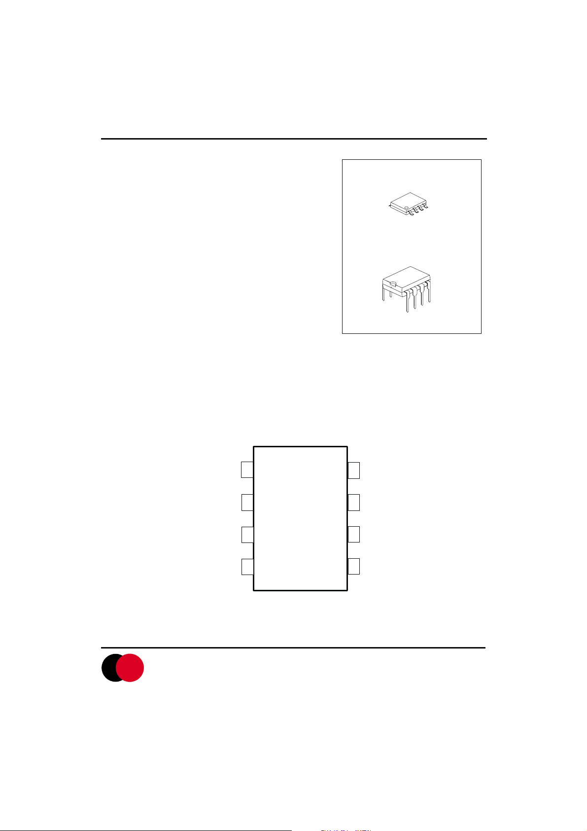
PIN CONFIGURATIONS
OUTPUT 1
1
SOP-8
DIP-8
8
Vcc+
CONTEK
INVERTING
INPUT 1
NON-
INVERTING
INPUT 1
Vcc-
2
Contek
TL062
3
4
OUTPUT2
7
INVERTING
6
INPUT 2
NON-
5
INVERTING
INPUT 2
Contek Microelectronics Co.,Ltd.
http://www.contek-ic.com E-mail:sales@contek-ic.com
1
Page 2
TL062 LINEAR INTEGRATED CIRCUIT
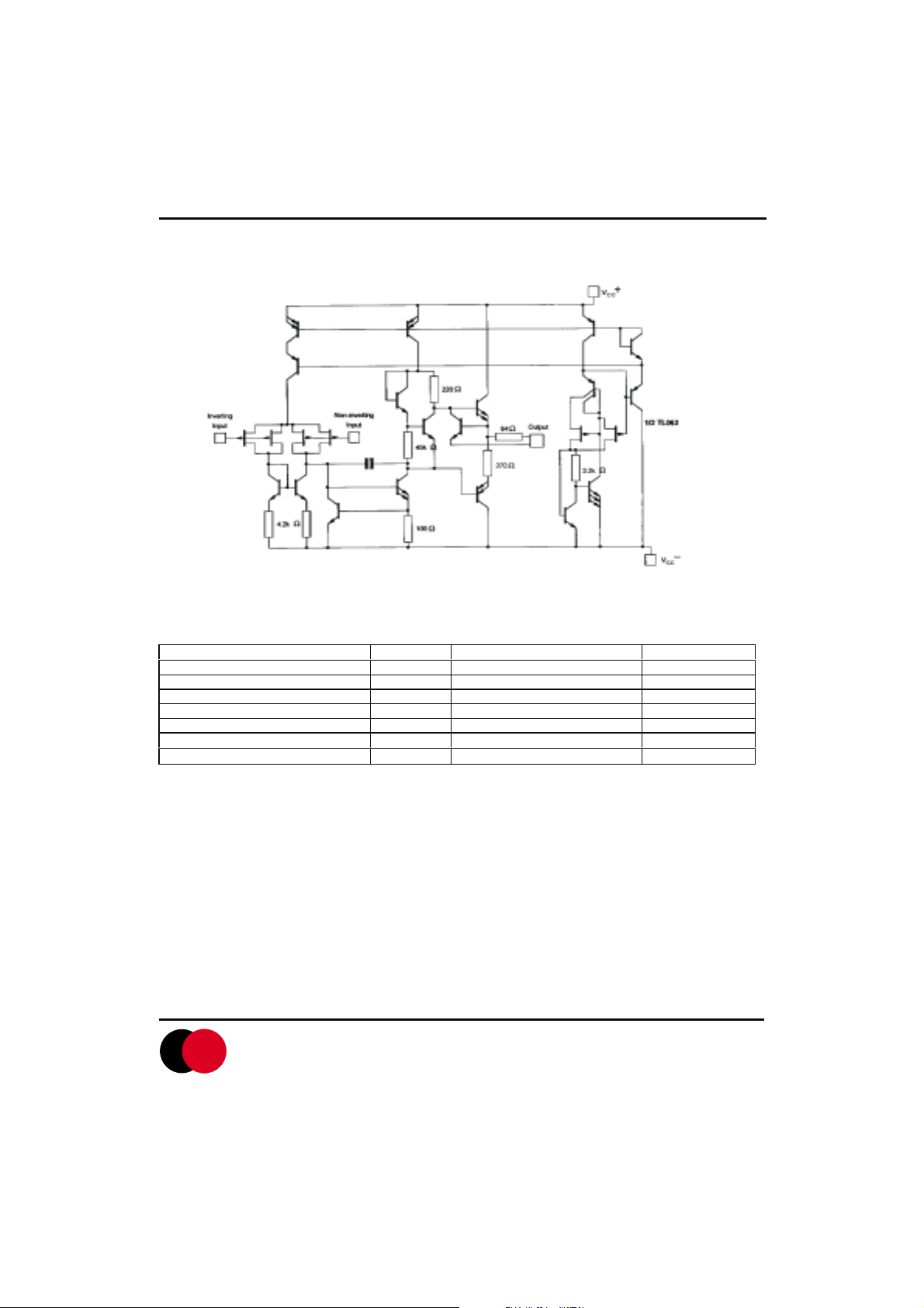
BLOCK DIAGRAM
ABSOLUTE MAXIMUM RATINGS(Ta=25 C )
Supply Voltage (note 1) Vcc +-18 V
Input Voltage (note 2) Vi +-15 V
Differential Input Voltage (note 3) Vid +-30 V
Power Dissipation Ptot 680 mW
Output Short-Circuit Duration (Note 4) Infinite
Operating Free Air Temperature Toper 0 to 70
Storage Temperature Tstg -65 to 150
PARAMETER SYMBOL VALUE UNIT
C
C
NOTES: 1. All voltage values, except differential voltage, are with respect to the zero reference level (ground) of
the supply voltages where the zero reference level is the midpoint between Vcc- and Vcc+.
2. The magnitude of the input voltage must never exceed the magnitude of the supply voltage or 15 volts,
whichever is less.
3. Differential voltages are at the non-inverting input terminal with respect to the inverting input terminal.
4. The output may be shorted to ground or to either supply. Temperature and/or supply voltages must be
limited to ensure that the dissipation rating is not exceeded.
Contek Microelectronics Co.,Ltd.
CONTEK
http://www.contek-ic.com E-mail:sales@contek-ic.com
2
Page 3
TL062 LINEAR INTEGRATED CIRCUIT
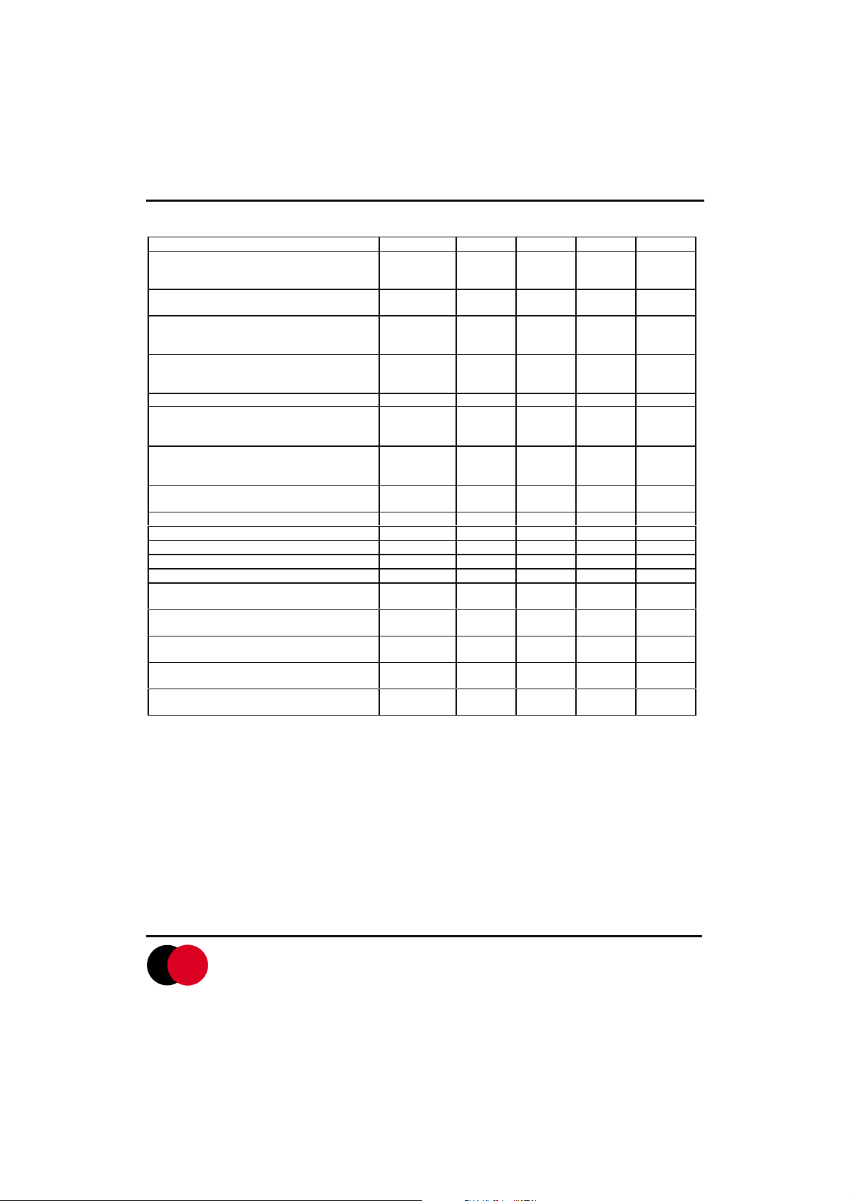
TL062 ELECTRICAL CHARACTERISTICS( Vcc=+-15V, Ta=25 C, unless otherwise specified)
PARAMETER SYMBOL MIN TYP MAX UNIT
Input Offset Voltage(Rs=50W), Ta=25 C
Tmin<=Ta<= Tmax
Temperature Coefficient of Input Offset
Voltage(Rs=50W)
Input Offset Current*
Ta=25 C
Tmin<=Ta<= Tmax
Input Bias Current*
Ta=25 C
Tmin<=Ta<= Tmax
Input Common Mode Voltage Vicm +-11 -12~+15 V
Output Voltage Swing(RL=10kW,CL=100pF)
Ta=25 C
Tmin<=Ta<= Tmax
Large Signal Voltage Gain(RL=10W, Vo=+10V) Ta=25 C
Tmin<=Ta<= Tmax
Gain Bandwidth Product(Ta=25 C, RL=10kW ,
C
L=100Pf)
Input Resistance Ri
Common Mode Rejection Ratio(RS=50W)
Supply Voltage Rejection Ratio(RS=50W)
Supply Current(Ta=25 C, no load, no signal)
Channel Separation(Av=100, Ta=25 C)
Total Power Consumption(Ta=25 C, no load,
no signal)
Slew Rate(Vi=10V, RL =10kW,CL=100pF,
Av=1)
Rise Time(Vi=20mV, RL=10kW,CL=100pF,
Av=1)
Overshoot Factor(Vi=20mV, RL=10kW,
L=100pF, Av=1)
C
Equivalent Input Noise Voltage(RS=100W ,
f=1KHz)
*The Input bias currents of a FET-input operational amplifier are normal junction reverse currents, which are
temperature sensitive. Pulse techniques must be used that will maintain the junction temperature as closes to the
ambient temperature as possible.
Vio
Dvio 10
Iio
Iib
Vopp
Avd
GBP 1 MHz
CMR 70 76 dB
SVR 70 95 dB
Icc 200 250
01/V02 120 dB
V
P
D 6 7.5 mW
SR 1.5 3.5
t
r 0.2
Kov 10 %
e
n 42
20
20
3
3
315
20
5 200
5
30 400
10
27 V
6 V/mV
1012
mV
mV/ C
pA
nA
pA
nA
W
mA
V/ms
ms
CONTEK
Contek Microelectronics Co.,Ltd.
http://www.contek-ic.com E-mail:sales@contek-ic.com
3
Page 4

TL062 LINEAR INTEGRATED CIRCUIT
ContekTL062AC ELECTRICAL CHARACTERISTICS(Vcc=+-15V, Ta=25 C, unless otherwise
specified)
Input Offset Voltage(Rs=50W, Ta=25 C
PARAMETER SYMBOL MIN TYP MAX UNIT
Tmin<=Ta<= Tmax
Temperature Coefficient of Input Offset
Voltage(Rs=50W)
Input Offset Current*
Ta=25 C
Tmin<=Ta<= Tmax
Input Bias Current*
Ta=25 C
Tmin<=Ta<= Tmax
Input Common Mode Voltage Vicm +-11.5 -12~+15 V
Output Voltage Swing(RL=10kW)
Ta=25 C
Tmin<=Ta<= Tmax
Large Signal Voltage Gain(RL=10kW, Vo=+-
10V) Ta=25 C
Tmin<=Ta<= Tmax
Gain Bandwidth Product(Ta=25 C, RL=10kW ,
C
L=100pF)
Input Resistance Ri
Common Mode Rejection Ratio(RS=50W)
Supply Voltage Rejection Ratio(RS=50W)
Supply Current(Ta=25 C, no load, no signal)
Channel Separation(Av=100, Ta=25 C)
Total Power Consumption(Ta=25 C, no load,
no signal)
Slew Rate(Vi=10V, RL =10kW,CL=100pF,
Av=1)
Rise Time(Vi=20mV, RL=10kW,CL=100pF,
Av=1)
Overshoot Factor(Vi=20mV, RL=10kW,
C
L=100pF, Av=1)
Equivalent Input Noise Voltage(RS=100W ,
f=1KHz)
*The Input bias currents of a FET-input operational amplifier are normal junction reverse currents, which are
temperature sensitive. Pulse techniques must be used that will maintain the junction temperature as closes to the
ambient temperature as possible.
Vio
Dvio 10
Iio
Iib
Vopp
Avd
GBP 1 MHz
CMR 80 86 dB
SVR 80 95 dB
Icc 200 250
01/V02 120 dB
V
P
D 6 7.5 mW
SR 1.5 3.5
t
r 0.2
Kov 10 %
e
n 42
20
20
4
4
36
7.5
mV/ C
5 100
3
30 200
7
27 V
6 V/mV
1012
mV
pA
nA
pA
nA
W
mA
V/ms
ms
CONTEK
Contek Microelectronics Co.,Ltd.
http://www.contek-ic.com E-mail:sales@contek-ic.com
4
Page 5

TL062 LINEAR INTEGRATED CIRCUIT
Contek TL062BC ELECTRICAL CHARACTERISTICS( Vcc=+-15V, Ta=25 C, unless otherwise
specified)
Input Offset Voltage(Rs=50W, Ta=25 C
PARAMETER SYMBOL MIN TYP MAX UNIT
Tmin<=Ta<= Tmax
Temperature Coefficient of Input Offset
Voltage(Rs=50W)
Input Offset Current*
Ta=25 C
Tmin<=Ta<= Tmax
Input Bias Current*
Ta=25 C
Tmin<=Ta<= Tmax
Input Common Mode Voltage Vicm +-11 -12~+15 V
Output Voltage Swing(RL=10kW)
Ta=25 C
Tmin<=Ta<= Tmax
Large Signal Voltage Gain(RL=10kW, Vo=+10V) Ta=25 C
Tmin<=Ta<= Tmax
Gain Bandwidth Product(Ta=25 C, RL=10kW ,
C
L=100pF)
Input Resistance Ri
Common Mode Rejection Ratio(RS=50W)
Supply Voltage Rejection Ratio(RS=50W)
Supply Current(Ta=25 C, no load, no signal)
Channel Separation(Av=100, Ta=25 C)
Total Power Consumption(Ta=25 C, no load,
no signal)
Slew Rate(Vi=10V, RL =10kW,CL=100pF,
Av=1)
Rise Time(Vi=20mV, RL=10kW,CL=100pF,
Av=1)
Overshoot Factor(Vi=20mV, RL=10kW,
C
L=100pF, Av=1)
Equivalent Input Noise Voltage(RS=100W ,
f=1KHz)
*The Input bias currents of a FET-input operational amplifier are normal junction reverse currents, which are
temperature sensitive. Pulse techniques must be used that will maintain the junction temperature as closes to the
ambient temperature as possible.
Vio
Dvio 10
Iio
Iib
Vopp
Avd
GBP 1 MHz
CMR 80 86 dB
SVR 80 95 dB
Icc 200 250
01/V02 120 dB
V
P
D 6 7.5 mW
SR 1.5 3.5
t
r 0.2
Kov 10 %
e
n 42
20
20
4
4
23
5
mV/ C
5 100
3
30 200
7
27 V
6 V/mV
1012
mV
pA
nA
pA
nA
W
mA
V/ms
ms
CONTEK
Contek Microelectronics Co.,Ltd.
http://www.contek-ic.com E-mail:sales@contek-ic.com
5
Page 6

TL062 LINEAR INTEGRATED CIRCUIT
CONTEK
Contek Microelectronics Co.,Ltd.
http://www.contek-ic.com E-mail:sales@contek-ic.com
6
Page 7

TL062 LINEAR INTEGRATED CIRCUIT
CONTEK
Contek Microelectronics Co.,Ltd.
http://www.contek-ic.com E-mail:sales@contek-ic.com
7
Page 8

TL062 LINEAR INTEGRATED CIRCUIT
PARAMETER MEASUREMENT INFORMATION
CONTEK
Contek Microelectronics Co.,Ltd.
http://www.contek-ic.com E-mail:sales@contek-ic.com
8
 Loading...