

Page 1
TK715xxAS
LOW DROPOUT VOLTAGE REGULATOR
FEATURES
n High Voltage Precision at ± 2.0% or ± 60 mV
n Very Low Quiescent Current
n Very Low Dropout Voltage
n Reverse Voltage Protection
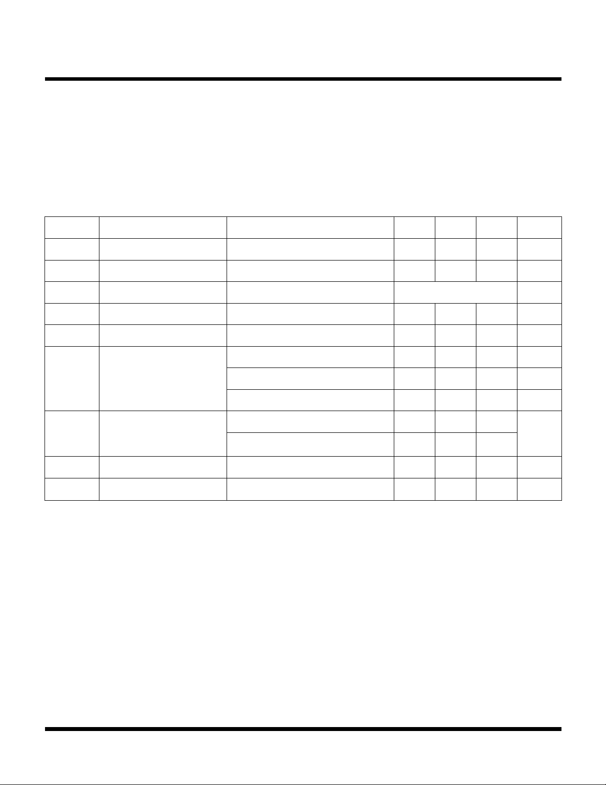
n Miniature Package (SOT23-3)
n Short Circuit Protection
n High Ripple Rejection
n Can use Multilayer Ceramic Capacitors
DESCRIPTION
The TK715xx is a low dropout linear regulator housed in a
small SOT23-3 package, rated at 400 mW. An internal
PNP transistor is used to achieve a low dropout voltage of
105 mV (typ.) at 50 mA load current. This device offers
high precision output voltage of ± 2.0 % or ± 60 mV. The
TK715xx has a very low quiescent current of 25 µA (typ.)
at no load. The low quiescent current and dropout voltage
make this part ideal for battery powered applications. The
internal reverse bias protection eliminates the requirement
for a reverse voltage protection diode, saving cost and
board space. The high 60 dB ripple rejection and low noise
provide enhanced performance for critical applications.
APPLICATIONS
n Battery Powered Systems
n Cellular Telephones
n Pagers
n Personal Communications Equipment
n Portable Instrumentation
n Portable Consumer Equipment
n Radio Control Systems
n Toys
n Low Voltage Systems
TK715xxAS
V
OUT
30T
V
IN
20P
ORDERING INFORMATION
Voltage Code
VOLTAGE CODE
15 = 1.5 V 35 = 3.5 V
16 = 1.6 V 36 = 3.6 V
17 = 1.7 V 37 = 3.7 V
18 = 1.8 V 38 = 3.8 V
19 = 1.9 V 39 = 3.9 V
20 = 2.0 V 40 = 4.0 V
21 = 2.1 V 41 = 4.1 V
22 = 2.2 V 42 = 4.2 V
23 = 2.3 V 43 = 4.3 V
24 = 2.4 V 44 = 4.4 V
25 = 2.5 V 45 = 4.5 V
26 = 2.6 V 46 = 4.6 V
27 = 2.7 V 47 = 4.7 V
28 = 2.8 V 48 = 4.8 V
29 = 2.9 V 49 = 4.9 V
30 = 3.0 V 50 = 5.0 V
31 = 3.1 V 60 = 6.0 V
32 = 3.2 V 70 = 7.0 V
33 = 3.3 V 80 = 8.0 V
34 = 3.4 V 90 = 9.0 V
TK715 ASCL
TEMPERATURE CODE
C -30 to +80 °C
PACKAGE CODE
S : SOT-23-3
Tape/ Reel Code
Temp. Code
Package Code
TAPE/REEL CODE
L: Tape Left
GND
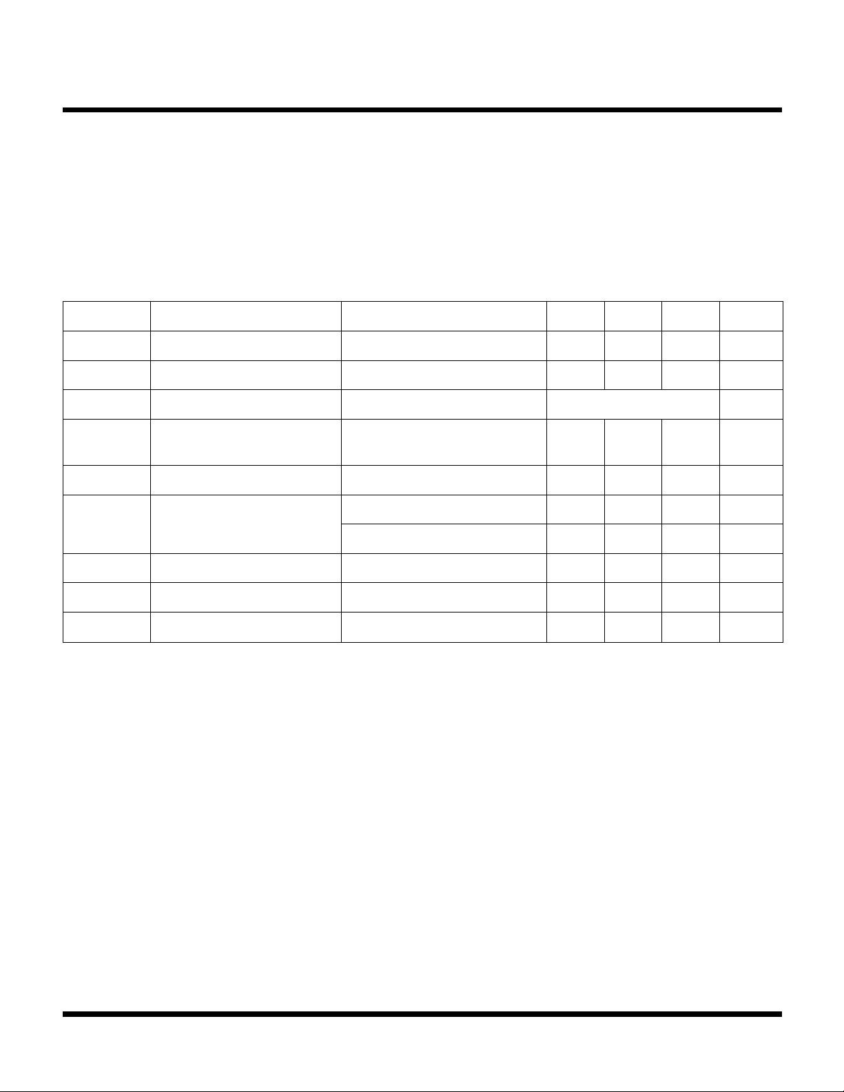
BLOCK DIAGRAM
V
IN
THERMAL
PROTECTION
+
BANDGAP
REFERENCE
GND
-
+
V
OUT
March 2001 TOKO, Inc. Page 1
Page 2
TK715xxAS
ABSOLUTE MAXIMUM RATINGS (V
Supply Voltage .............................................-0.4 to 19 V
Power Dissipation (Note 1)................................400 mW
Reverse Bias ............................................................. 8 V
Short Circuit Current........................................... 170 mA
Storage Temperature (Ambient).............. -55 to +150 °C
£ 5.0 V)
OUT
Operating Temperature (Ambient) ............ -30 to +80 °C
Max. Operating Temperature (Junction) ............. 125 °C
Operating Voltage Range........................... 1.8 to 18.0 V
Junction Temperature ......................................... 150 °C
Lead Soldering Temperature (10 s)..................... 235 °C
TK715xx ELECTRICAL CHARACTERISTICS (V
Test conditions: VIN = V
LOBMYSRETEMARAPSNOITIDNOCTSETNIMPYTXAMSTINU
I
Q
I
DNG
V
TUO
geReniLnoitalugeReniLV
geRdaoLnoitalugeRdaoLI
V
PORD
OUT(TYP)
+ 1V, TA = 25 °C, unless otherwise specified.
tnerruCtnecseiuQI
tnerruCniPdnuorGI
egatloVtuptuOI
)5etoN(egatloVtuoporD
TUO
TUO
TUO
NI
TUO
I
TUO
I
TUO
Am0=5254Aµ
Am51=003005Aµ
Am5=1elbaTeeSV
V=
)PYT(TUO
VotV1+
Am05=501.081.0V
V4.2,Am001= £ V
£ 5.0 V)
OUT
V6+321Vm
)PYT(TUO
)2etoN(,Am001ot5=8163Vm
£ V0.561.082.0V
TUO
I
TUO
V1.2,Am001= £ V
£ V4.261.003.0V
TUO
511551
I
)XAM(TUO
tnerruCtuptuOsuounitnoC
8.1
V £ Vni£ )3etoN(V1.2
0709
RRnoitcejeRelppiR)4etoN(06Bd
/ ∆T
∆V
TUO
Note 1: Power dissipation is 400 mW when mounted as recommended. Derate at 3.2 mW/°C for operation above 25 °C.
Note 2: Refer to “Definition of Terms.”
Note 3: Please refer to the Applications Section for more information.
Note 4: Ripple rejection is measured at VR = 200 mVrms, VIN = V
Note 5: The minimum operating voltage for VIN can be 1.8 V. Also, the minimum voltage required for VIN is VIN = V
V
£ 2.0 V at the minimum input operating voltage is not preferred.
OUT
Gen. Note: Parameters with min. or max. values are 100% tested at TA = 25 °C.
tneiciffeoCerutarepmeTI
TUO
Am5=03C°/mpp
OUT(TYP)
+ 2 V, I
= 10 mA, CL = 2.2 µF, f = 100 Hz.
OUT
DROP
+ V
. As a result, operating at
OUT
Am
Page 2 March 2001 TOKO, Inc.
Page 3
TK715xxAS
ABSOLUTE MAXIMUM RATINGS (V
Supply Voltage .............................................-0.4 to 19 V
Power Dissipation (Note 1)................................400 mW
Reverse Bias ............................................................. 8 V
Short Circuit Current........................................... 170 mA
Storage Temperature (Ambient).............. -55 to +150 °C
³ 5.1 V)
OUT
Operating Temperature (Ambient) ............ -30 to +80 °C
Max. Operating Temperature (Junction) ............. 125 °C
Operating Voltage Range.............................. 1.8 to 18 V
Junction Temperature ......................................... 150 °C
Lead Soldering Temperature (10 s)..................... 235 °C
TK715xx ELECTRICAL CHARACTERISTICS (V
Test conditions: VIN = V
LOBMYSRETEMARAPSNOITIDNOCTSETNIMPYTXAMSTINU
I
Q
I
DNG
V
TUO
geReniLnoitalugeReniL
geRdaoLnoitalugeRdaoLI
V
PORD
OUT(TYP)
+ 1V, TA = 25 °C, unless otherwise specified.
tnerruCtnecseiuQI
tnerruCniPdnuorGI
egatloVtuptuOI
TUO
TUO
TUO
V
NI
V
TUO
I
egatloVtuoporD
TUO
I
TUO
Am0=2306Aµ
Am51=003005Aµ
Am5=1elbaTeeSV
V=
)PYT(TUO
)PYT(TUO
otV1+
Am05=501.081.0V
Am001=061.082.0V
³ 5.1 V)
OUT
V81xaMroV6+
321Vm
)2etoN(,Am001ot5=5308Vm
I
)XAM(TUO
tnerruCtuptuOsuounitnoC511551Am
RRnoitcejeRelppiR)3etoN(06Bd
/ ∆T
∆V
TUO
Note 1: Power dissipation is 400 mW when mounted as recommended. Derate at 3.2 mW/°C for operation above 25 °C.
Note 2: Refer to “Definition of Terms.”
Note 3: Ripple rejection is measured at VR = 200 mVrms, VIN = V
Gen. Note: Parameters with min. or max. values are 100% tested at TA = 25 °C.
tneiciffeoCerutarepmeTI
TUO
Am5=03C°/mpp
OUT(TYP)
+ 2 V, I
= 10 mA, CL = 2.2 µF, f = 100 Hz.
OUT
March 2001 TOKO, Inc. Page 3
Page 4
TK715xxAS
TK715xxAS ELECTRICAL CHARACTERISTICS TABLE 1
Output Voltage V
Voltage Code Voltage
OUT(MIN)
V
OUT(MAX)
Test
1.5 V 15 1.440 V 1.560 V 2.5 V
1.6 V 16 1.540 V 1.660 V 2.6 V
1.7 V 17 1.640 V 1.760 V 2.7 V
1.8 V 18 1.740 V 1.860 V 2.8 V
1.9 V 19 1.840 V 1.960 V 2.9 V
2.0 V 20 1.940 V 2.060 V 3.0 V
2.1 V 21 2.040 V 2.160 V 3.1 V
2.2 V 22 2.140 V 2.260 V 3.2 V
2.3 V 23 2.240 V 2.360 V 3.3 V
2.4 V 24 2.340 V 2.460 V 3.4 V
2.5 V 25 2.440 V 2.560 V 3.5 V
2.6 V 26 2.540 V 2.660 V 3.6 V
2.7 V 27 2.640 V 2.760 V 3.7 V
2.8 V 28 2.740 V 2.860 V 3.8 V
2.9 V 29 2.840 V 2.960 V 3.9 V
3.0 V 30 2.940 V 3.060 V 4.0 V
3.1 V 31 3.040 V 3.160 V 4.1 V
3.2 V 32 3.140 V 3.260 V 4.2 V
3.3 V 33 3.240 V 3.360 V 4.3 V
3.4 V 34 3.340 V 3.460 V 4.4 V
Output Voltage V
Voltage Code Voltage
OUT(MIN)
V
OUT(MAX)
Test
3.5 V 35 3.440 V 3.560 V 4.5 V
3.6 V 36 3.530 V 3.670 V 4.6 V
3.7 V 37 3.630 V 3.770 V 4.7 V
3.8 V 38 3.730 V 3.870 V 4.8 V
3.9 V 39 3.830 V 3.970 V 4.9 V
4.0 V 40 3.930 V 4.070 V 5.0 V
4.1 V 41 4.030 V 4.170 V 5.1 V
4.2 V 42 4.130 V 4.270 V 5.2 V
4.3 V 43 4.230 V 4.370 V 5.3 V
4.4 V 44 4.330 V 4.470 V 5.4 V
4.5 V 45 4.430 V 4.570 V 5.5 V
4.6 V 46 4.530 V 4.670 V 5.6 V
4.7 V 47 4.630 V 4.770 V 5.7 V
4.8 V 48 4.730 V 4.870 V 5.8 V
4.9 V 49 4.830 V 4.970 V 5.9 V
5.0 V 50 4.930 V 5.070 V 6.0 V
6.0 V 60 5.880 V 6.120 V 7.0 V
7.0 V 70 6.860 V 7.140 V 8.0 V
8.0 V 80 7.840 V 8.160 V 9.0 V
9.0 V 90 8.820 V 9.180 V 10.0 V
Page 4 March 2001 TOKO, Inc.
Page 5
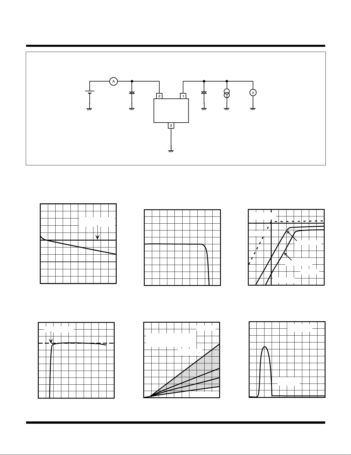
TEST CIRCUIT
I
IN
V
IN
C
IN
0.1 µF
V
IN
GND
V
OUT
C
L
1.0 µF
TANTALUM
I
OUT
TYPICAL PERFORMANCE CHARACTERISTICS
TA = 25 °C, unless otherwise specified.
TK715xxAS
V
OUT
(10 mV/ DIV)
OUT
V
(50 mV/ DIV)
OUT
V
0 10 20
LOAD REGULATION
0 50 100
LINE REGULATION
V
TYPICAL
OUT
I
OUT
VIN (V)
V
OUT
(mA)
TYPICAL
SHORT CIRCUIT CURRENT
5
4
(V)
3
OUT
V
2
1
0
0 100 200
I
OUT
(mA)
REVERSE BIAS CURRENT RANGE
100
Because the output voltage is
different, the reverse current
will change this area.
80
V
= 2.0 V
60
(µA)
REV
I
40
OUT
20
0
0 5 10
V
REV
(V)
(VIN = 0 V)
V
= 8.0 V
OUT
OUTPUT VOLTAGE vs.
INPUT VOLTAGE
V
TYPICAL
I
= 50 mA
OUT
I
OUT
OUT
= 0 mA
(25 mV/ DIV)
I
OUT
V
VIN = V
OUT
OUT
= 100 mA
50 mV/DIV
0
V
(V)
IN
INPUT CURRENT
VS.
INPUT VOLTAGE
I
= 0 mA
V
= 3 V
OUT
VIN (V)
OUT
2
(mA)
1
Q
I
0
0 5 10
March 2001 TOKO, Inc. Page 5
Page 6

TK715xxAS
I
GND
(µA)
200
500
GROUND PIN CURRENT vs.
OUTPUT CURRENT
I
OUT
(mA)
100
0 5 10 15
400
300
0
TYPICAL PERFORMANCE CHARACTERISTICS (CONT.)
TA = 25 °C, unless otherwise specified.
DROPOUT VOLTAGE
OUTPUT CURRENT
0
(mV)
-100
DROP
V
-200
0 50 100
I
OUT
(mA)
GROUND PIN CURRENT vs.
OUTPUT CURRENT
5
4
3
(mA)
GND
I
2
1
0
0 20 40 60 80 100
I
OUT
(mA)
VS.
DROPOUT VOLTAGE
VS.
TEMPERATURE
250
200
(mV)
150
DROP
V
100
I
OUT
= 100 mA
I
OUT
= 50 mA
50
0
-50 0 50 100
TA(°C)
OUTPUT VOLTAGE
VS.
TEMPERATURE
20
10
(mV)
OUT
-10
∆V
0
3.0 V
-20
-30
-50 0 50 100
TA (°C)
MAX OUTPUT CURRENT
180
160
(mA)
140
OUT
I
3.0 V
120
100
0
-50 0 50 100
TA (°C)
Ripple Rejection
0
-10
-20
-30
-40
-50
dB
-60
-70
-80
-90
-100
0.01 0.1 1 10 100 1000
Page 6 March 2001 TOKO, Inc.
RIPPLE REJECTION
----TANTALUM
1.0 µF : 4.7 µF
I
= 10 mA
OUT
CERAMIC
2.2 µF : 4.7 µF
F (kHz)
V
IN
715xxA
0.1 µF
(TANTALUM OR CERAMIC)
GND
RIPPLE REJECTION CIRCUIT
V
OUT
C
1.0 µF
2.2 µF
4.7 µF
L
Page 7

Output Noise
TK715xxAS
TYPICAL PERFORMANCE CHARACTERISTICS (CONT.)
TA = 25 °C, unless otherwise specified.
NOISE LEVEL (TK71530A)
OUTPUT CURRENT
250
200
CL = 2.2 µF
CL = 4.7 µF
150
NOISE (µV)
100
50
0
1.0 5.0 10
BW = 400 Hz~80 KHz
I
(mA)
OUT
Load & Line Response
LINE VOLTAGE STEP RESPONSE
V
+ 2V
V
IN
OUT
CL = 1.0 µF
25 µS/DIV
CL = 1 µF
CL = 10 µF
V
OUT
VS.
+ 1V
I
OUT
LOAD CURRENT
STEP RESPONSE
5 mA
V
IN
715xxA
0.1 µF
GND
OUTPUT NOISE CIRCUIT
50 mA
CL = 1.0 µF
25 µS/DIV
V
OUT
(TANTALUM)
C
1.0 µF
2.2 µF
4.7 µF
10 µF
L
V
OUT
I
OUT
50 mV/DIV
= 10mA
V
OUT
50 mV/DIV
Note: To improve the load and line transient response, increase the value of the output capacitor.
March 2001 TOKO, Inc. Page 7
Page 8

TK715xxAS
DEFINITION AND EXPLANATION OF TECHNICAL TERMS
OUTPUT VOLTAGE (V
The output voltage is specified with V
and I
= 5 mA.
OUT
DROPOUT VOLTAGE (V
OUT
)
DROP
IN
= (V
OUT(TYP)
+ 1 V)
)
The dropout voltage is the difference between the input
voltage and the output voltage at which point the regulator
starts to fall out of regulation. Below this value, the output
voltage will fall as the input voltage is reduced. It is
dependent upon the load current and the junction temperature.
CONTINUOUS OUTPUT CURRENT (I
OUT
)
Normal operating output current. This is limited by package power dissipation.
LINE REGULATION (Line Reg)
Line regulation is the ability of the regulator to maintain a
constant output voltage as the input voltage changes. The
line regulation is specified as the input voltage is changed
from VIN = V
OUT(TYP)
+ 1 V to VIN = V
OUT(TYP)
+ 6 V or VIN =
max 18 V.
LOAD REGULATION (Load Reg)
RIPPLE REJECTION RATIO (RR)
Ripple rejection is the ability of the regulator to attenuate
the ripple content of the input voltage at the output. It is
specified with 200 mVrms, 100 Hz superimposed on the
input voltage, where V
IN
= V
OUT(TYP)
+ 2.0 V. The output
decoupling capacitor is set to 2.2 µF and the load current
is set to 10 mA. Ripple rejection is the ratio of the ripple
content of the output vs. the input and is expressed in dB.
REVERSE VOLTAGE PROTECTION
Reverse voltage protection prevents damage due to the
output voltage being higher than the input voltage. This
fault condition can occur when the output capacitor remains charged and the input is reduced to zero, or when
an external voltage higher than the input voltage is applied
to the output side.
REDUCTION OF OUTPUT NOISE
Although the architecture of the Toko regulators are designed to minimize semiconductor noise, further reduction
can be achieved by the selection of external components.
The obvious solution is to increase the size of the output
capacitor. Please note that several parameters are affected by the value of the capacitors and bench testing is
recommended when deviating from standard values.
Load regulation is the ability of the regulator to maintain a
PACKAGE POWER DISSIPATION (P
)
D
constant output voltage as the load current changes. It is
a pulsed measurement to minimize temperature effects
with the input voltage set to VIN = V
OUT(TYP)
+1 V. The load
regulation is specified under the output current step condition 5 mA to 100 mA.
This is the power dissipation level at which the thermal
sensor is activated. The IC contains an internal thermal
sensor which monitors the junction temperature. When the
junction temperature exceeds the monitor threshold of
150 °C, the IC is shut down. The junction temperature
QUIESCENT CURRENT (IQ)
The quiescent current is the current which flows through
the ground terminal under no load conditions (I
= 0 mA).
OUT
rises as the difference between the input power (VIN x IIN)
and the output power (V
OUT
x I
) increases. The rate of
OUT
temperature rise is greatly affected by the mounting pad
configuration on the PCB, the board material, and the
ambient temperature. When the IC mounting has good
GROUND CURRENT (I
GND
)
thermal conductivity, the junction temperature will be low
even if the power dissipation is great. When mounted on
Ground current is the current which flows through the
ground pin(s). It is defined as IIN - I
, excluding control
OUT
current.
the recommended mounting pad, the power dissipation of
the SOT23-3 is increased to 400 mW. For operation at
ambient temperatures over 25 °C, the power dissipation of
the SOT23-3 device should be derated at 3.2 mW/°C. To
Page 8 March 2001 TOKO, Inc.
Page 9

TK715xxAS
DEFINITION AND EXPLANATION OF TECHNICAL TERMS (CONT.)
determine the power dissipation for shutdown when
mounted, attach the device on the actual PCB and deliberately increase the output current (or raise the input
voltage) until the thermal protection circuit is activated.
Calculate the power dissipation of the device by subtracting the output power from the input power. These measurements should allow for the ambient temperature of the
PCB. The value obtained from P
/(150 °C - TA) is the
D
derating factor. The PCB mounting pad should provide
maximum thermal conductivity in order to maintain low
device temperatures. As a general rule, the lower the
temperature, the better the reliability of the device. The
thermal resistance when mounted is expressed as follows:
Tj = 0jA x PD + T
A
For Toko ICs, the internal limit for junction temperature is
150 °C. If the ambient temperature (TA) is 25 °C, then:
150 °C = 0jA x PD + 25 °C
0jA = 125 °C/ P
D
2) PD1 is taken to be PD x (~ 0.8 - 0.9)
3) Plot P
4) Connect P
against 25 °C
D1
to the point corresponding to the 150
D1
°C with a straight line.
5) In design, take a vertical line from the maximum
operating temperature (e.g., 75 °C) to the derating curve.
6) Read off the value of PD against the point at which
the vertical line intersects the derating curve. This is taken
as the maximum power dissipation, DPD.
The maximum operating current is:
I
OUT
500
400
300
(mW)
D
P
200
100
= (D
PD
/ (V
IN(MAX) - VOUT
MOUNTED AS SHOWN
)
FREE AIR
PD is the value when the thermal sensor is activated. A
simple way to determine PD is to calculate VIN x IIN when
the output side is shorted. Input current gradually falls as
temperature rises. You should use the value when thermal
equilibrium is reached.
The range of usable currents can also be found from the
graph below.
(mW)
P
D
D
PD
3
6
4
5
25 50 75 150
TA (°C)
Procedure:
1) Find P
D
0
0 50 100 150
TA (°C)
SOT23-3 POWER DISSIPATION CURVE
March 2001 TOKO, Inc. Page 9
Page 10

TK715xxAS
APPLICATION INFORMATION
INPUT-OUTPUT CAPACITORS
Linear regulators require input and output capacitors in order to maintain regulator loop stability. The output capacitor
should be selected within the Equivalent Series Resistance (ESR) range as shown in the graphs below for stable
operation. The output capacitor C
increase as CL is reduced, so the largest value of CL possilbe is recommended (CL = 4.7 mF or more).
Note: It is very important to check the selected manufacturers electrical characteristics (capacitance and ESR) over
temperature.
MULTI LAYER CERAMIC CAP
5.0
can be reduced as the output voltage is increased. However, the output noise will
L
CIN = 0.1 µF
0.68 µF ≤ CL ≤ 4.7 µF or More
3.8
3.6
3.4
3.2
3.0
2.8
2.6
2.4
1.0 µF
2.2
2.0
1.8
1.6
1.5
0 20 40 60 80 100
UNSTABLE AREA UNDER
AND TO THE LEFT
CL = 0.68 µF
CL = 4.7 µF
3.3 µF
I
OUT
MLCC
(mA)
Range which can be used:
5.0
3.8
3.6
3.4
3.2
(V)
3.0
2.8
OUT
2.6
V
2.4
2.2
2.0
1.8
1.6
1.5
0 20 40 60 80 100
UNSTABLE AREA UNDER
AND TO THE LEFT
TANTALUM CAP
CL = 0.1 µF
CL = 0.22 µF (
0.1 µF
TANTALUM)
I
OUT
(mA)
MLCC
or More
2.2 µF
V
OUT
V
OUT
V
OUT
CIN = 0.1 µF
TANTALUM
or More
Stable area is
above the line
³ 2.8V I
³ 2.0V I
³ 1.5V I
Stable area is
above the line
ESR ≥ 0.01 Ω
= 1 mA ~ Max, MULTI LAYER CERAMIC CAP. ³ 0.68 mF
OUT
= 1 mA ~ Max, MULTI LAYER CERAMIC CAP. ³ 1.0 mF
OUT
= 1 mA ~ Max, MULTI LAYER CERAMIC CAP. ³ 4.7 mF
OUT
0.1 µF ≤ CL ≤ 0.22 µF or More
ESR ≥ 1.0 Ω
Range which can be used: V
³ 1.9V I
OUT
= 1 mA ~ Max, TANTALUM CAP. ³ 0.1 mF (CERAMIC CAP 0.22 mF
OUT
+ 2.2W
Capacitor used for evaluation: V
³ 1.5V I
OUT
= 1 mA ~ Max, TANTALUM CAP. ³ 0.22 mF (CERAMIC CAP 0.22
OUT
mF + 2.2W
Page 10 March 2001 TOKO, Inc.
Page 11

TK715xxAS
APPLICATION INFORMATION (CONT)
INPUT-OUTPUT CAPACITORS (CONT)
OUTPUT NOISE IMPROVEMENT
An RC filter can be added to the output stage of the regulator to reduce output noise when the input voltage is high and
the output current only makes small changes. Select a regulator with a slightly higher output voltage because the final
output voltage will be reduced by the RC filter. If the output current does make a large change, the output voltage will
change. The following table shows output noise, and output voltage for various values of R
device.
OUT
and C
using a 3.5 V
OUT
VIN = 4.0 V, CIN = 10 mF (aluminum electrolytic), C
V
IN
TK715xxA
V
OUT
CL = 2.2 µF
NOITIDNOCTNEMERUSAEMC(ROTICAPACEDISTUPTUO
I
TUO
I
TUO
Am04-02=0V005.3Vµ012Vµ051Vµ031SMR
R
TUO
V
TUO
Fµ01Fµ74Fµ001FµC
= (see table), R
OUT
R
OUT
C
OUT
OUT
LOAD ADJ.
I
= 20, 30, 40 mA
OUT
)STINU
TUO
= (see table)
TUO
Am0201 W V692.3Vµ67Vµ05Vµ04SMR
ESION
Am038.6 W V782.3Vµ88Vµ55Vµ84SMR
Am041.5 W V662.3Vµ001Vµ06Vµ84SMR
RIPPLE REJECTION RATIO
An RC filter can be added to the input stage of the regulator to increase the ripple rejection when the input voltage is high.
Even if the resulting difference between VIN at the regulator (after the RC filter) and V
is small the TK71533AS will
OUT
output a stable voltage. The voltage dropped across the RC filter depends on the value of the input ripple noise. Select
the value of RIN such that the lowest value of VIN plus the ripple noise after the RC filter (peak to peak) is the output voltage
plus 0.2 V.
R
IN
V
IN
TK715xxA
C
IN
V
OUT
C
L
LOAD ADJ.
I
= 20, 30, 40 mA
OUT
March 2001 TOKO, Inc. Page 11
Page 12

TK715xxAS
APPLICATION INFORMATION (CONT)
R(*) MAG -17.98 dB 10 dB/ -50.00 dB
B(*) B -41.05 dB 10 dB/ -50.00 dB
FILTER
RIN = 27 Ω CIN = 47 µF
START: 100 Hz STOP: 1 MHz
OUT (B): -20.00 dBm ST: AUTO x1 1 MΩ
IRG: 26 dBm RBW: 30 kHZ VBW: 38 kHz
100
90
80
70
60
CAPACITANCE (%)
50
VOLTAGE DEPENDENCY
B CURVE
F CURVE
R(*) MAG -57.78 dB 10 dB/ -50.00 dB
B(*) B -41.05 dB 10 dB/ -50.00 dB
TK71533
FILTER + TK71533
RIN = 27 Ω CIN = 47 µF CL = 10 µF
START: 100 Hz STOP: 1 MHz
OUT (B): -20.00 dBm ST: AUTO x1 1 MΩ
IRG: 26 dBm RBW: 30 kHZ VBW: 38 kHz
100
90
80
70
60
CAPACITANCE (%)
50
TEMPERATURE DEPENDENCY
B CURVE
F CURVE
40
0 2 4 6 8 10
BIAS V (V)
-50 -25 0 25 50 75 100
TA (°C)
In general, a ceramic capacitor has a voltage and temperature dependence. Parts should be selected with consideration
of the voltage and temperature used. The “B” characteristic curves are recommended.
Page 12 March 2001 TOKO, Inc.
Page 13

TK715xxAS
APPLICATION INFORMATION (CONT .)
BOARD LAYOUT
The copper pattern should be as large as possible. Power dissipation is 400 mW for the SOT23-3, derated at 3.2 mW/°C for
operation above T
The internal reverse bias protection eliminates the requirement for a reverse voltage protection diode. This saves both
cost and board space.
= 25°C (qja = 312°C/W)
A
SOT23-3 BOARD LAYOUT
V
IN
500
400
300
D(mW)
P
200
FREE AIR
GND
RECOMMENDED AS SHOWN
++
V
OUT
100
March 2001 TOKO, Inc. Page 13
Page 14

TK715xxAS
TK715xxA
V
IN
V
OUT
0.22 µF
150 Ω
V
IN
3.3 µF
V
APPLICATION INFORMATION (CONT .)
REVERSE VOLTAGE PROTECTION
The internal reverse bias protection eliminates the requirement for a reverse voltage protection diode. This saves
both cost and board space.
V
IN
715xxAS
GND
V
OUT
Another reverse voltage protection technique is illustrated
below. The extra diode and extra capacitor are not necessary with the TK715xxA. The high output voltage accuracy
is maintained because the diode forward voltage variations over temperature and load current have been eliminated.
V
IN
TK715xxAS
V
OUT
SWITCHING OPERATION
Even though the input voltages or the output voltages are
different, the outputs of the TK715xxA regulators can be
connected together, and the output voltages switched. If
two or more TK715xxA regulators are turned ON simultaneously, the highest output voltage will be present.
V
IN
V
IN
TK71530A
TK71528A
V
OUT
3.0 OR 2.8
CURRENT BOOST OPERATION
The output current can be increased by connecting an
external PNP transistor as shown below. The output
current capability depends upon the H
of the external
fe
transistor. Note: The TK715xxA internal short circuit protection and thermal sensor do not protect the external
transistor.
PARALLEL OPERATION
The series resistor R is put in the input line of the low output
voltage regulator in order to prevent overdissipation. The
voltage dropped across the resistor reduces the large
input-to-output voltage across the regulator, reducing the
power dissipation in the device.
V
IN
R
Page 14 March 2001 TOKO, Inc.
TK71550A
TK71530A
TK71520A
5 V
3 V
2 V
Page 15

SOT23-3
TK715xxAS
PACKAGE OUTLINE
Marking Information
Product Code T Voltage Code
3
VOLTAGE CODE
0.4
e
e
0.95
1
Dimensions are shown in millimeters
Tolerance: x.x = ± 0.2 mm (unless otherwise specified)
0.95
2
2.9
0.1
Marking
PRODUCT CODE
+ 0.15
0.05
0.8
1.0
2.4
e1
e
e
0.95
0.95
e1
1.90
C1
0.1
±0.1
1.1
1.3 max
+ 0.15
0.05
0 ~ 0.1
Recommended Mounting Pad
0.15
1.6
15°max
0.4
±0.3
2.8
Toko America, Inc. Headquarters
1250 Feehanville Drive, Mount Prospect, Illinois 60056
Tel: (847) 297-0070 Fax: (847) 699-7864
TK71515S 15
TK71516S 16
TK71517S 17
TK71518S 18
TK71519S 19
TK71520S 20
TK71521S 21
TK71522S 22
TK71523S 23
TK71524S 24
TK71525S 25
TK71526S 26
TK71527S 27
TK71528S 28
TK71529S 29
TK71530S 30
TK71531S 31
TK71532S 32
TK71533S 33
TK71534S 34
TK71535S 35
TK71536S 36
TK71537S 37
TK71538S 38
TK71539S 39
TK71540S 40
TK71541S 41
TK71542S 42
TK71543S 43
TK71544S 44
TK71545S 45
TK71546S 46
TK71547S 47
TK71548S 48
TK71549S 49
TK71550S 50
TK71560S 60
TK71570S 70
TK71580S 80
TK71590S 90
TOKO AMERICA REGIONAL OFFICES
Midwest Regional Office
Toko America, Inc.
1250 Feehanville Drive
Mount Prospect, IL 60056
Tel: (847) 297-0070
Fax: (847) 699-7864
Western Regional Office
Toko America, Inc.
2480 North First Street , Suite 260
San Jose, CA 95131
Tel: (408) 432-8281
Fax: (408) 943-9790
Semiconductor Technical Support
Toko Design Center
4755 Forge Road
Colorado Springs, CO 80907
Tel: (719) 528-2200
Fax: (719) 528-2375
Visit our Internet site at http://www.tokoam.com
The information furnished by TOKO, Inc. is believed to be accurate and reliable. However, TOKO reserves the right to make changes or improvements in the design, specification or manufacture of
its products without further notice. TOKO does not assume any liability arising from the application or use of any product or circuit described herein, nor for any infringements of patents or other rights
of third parties which may result from the use of its products. No license is granted by implication or otherwise under any patent or patent rights of TOKO, Inc.
March 2001 TOKO, Inc. Page 15
All Rights Reserved
IC-xxx-TK715xx
0798O0.0K
Printed in the USA© 1999 Toko, Inc.
Page 16

 Loading...