

Page 1
TK6592x
20P
MEDIUM EL LAMP DRIVER
FEATURES
■ High Ratio of Brightness / Input Power
■ Constant Brightness Versus Input Supply Changes
■ Optimized for 9 nf to 27 nf Panel Capacitance
■ Panel Voltage Slew Rates Controlled for Life
Enhancement
■ Panel Peak to Peak Voltage Independent of Input
Voltage and Temperature
■ Panel Peak to Peak Frequency Independent of
Input Voltage and Temperature
■ Miniature Package (SOT23L-6)
■ Operates with Miniature Coil
■ Minimum External Components
■ Laser-Trimmed Fixed Frequency Operation
■ PWM Control Method
■ Adjustable Output Voltage
■ Lower Noise (Audio and EMI)
■ Split Power Supply Application
DESCRIPTION
The TK6592x Electroluminescent (EL) Lamp Driver has
been optimized for battery controlled systems where power
consumption and size are primary concerns. The miniature
device size (SOT23L-6), together with the miniature Toko
EL coils (D32FU, D31FU, D52FU), further helps system
designers reduce the space required to drive the small EL
panels.
The proprietary architecture (detailed in the Theory of
Operation section) of the TK6592x provides a constant
output power to the lamp, independent of variations in the
battery voltage. This architecture allows the output voltage
to remain relatively constant as battery voltages decay,
without the need for directly sensing the high voltage
output of the EL driver.
ORDERING INFORMATION
TK6592 MTL
Lamp Frequency Code
LAMP FREQUENCY CODE
TK65920 175 Hz
TK65921* 200 Hz
TK65922 225 Hz
TK65923* 250 Hz
TK65924 275 Hz
TK65925* 300 Hz
TK65926 325 Hz
TK65927* 350 Hz
TK65928 375 Hz
TK65929* 400 Hz
* Consult factory for availability
of other frequencies.
TAPE/REEL CODE
TL: Tape Left
APPLICATIONS
■ Battery Powered Systems
■ Cellular Telephones
■ Pagers
■ LCD Modules
■ Wrist Watches
■ Consumer Electronics
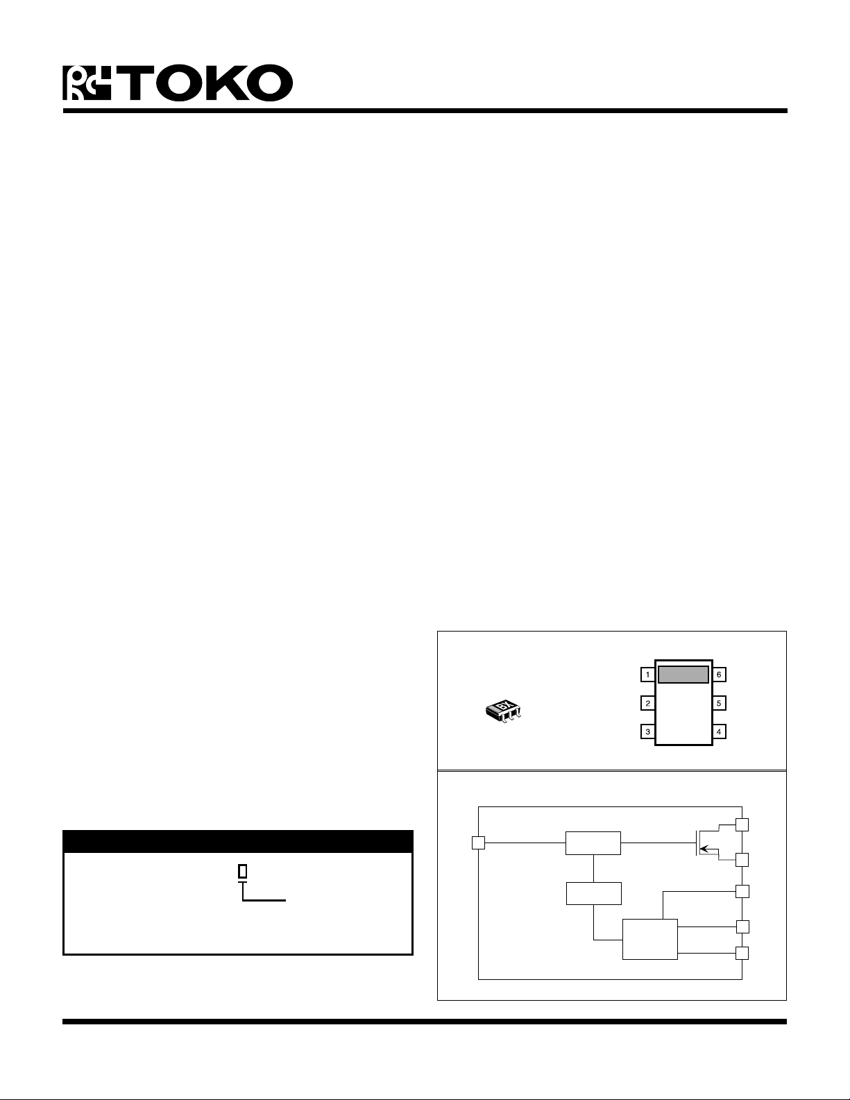
The oscillator circuits for the boost converter and lamp
driver are both internally generated in the TK6592x, without
the need for external components. The clock frequency of
the boost converter is laser-trimmed to ensure good initial
accuracy that is relatively insensitive to variations in
temperature and supply voltage. The clock frequency of
the lamp driver tracks the frequency of the boost converter
by a constant scaling factor.
Furthermore, the drive architecture of the TK6592x has
been designed to limit peak drive current delivered to the
lamp. This approach limits the slew rate of the voltage
across the lamp and has the potential to improve lamp life
and decrease RF interference.
The TK6592x is available in a miniature, 6-pin
SOT23L-6 surface mount package
TK6592x
+
EL
HV
-
EL
BLOCK DIAGRAM
V
CC
HV BOOST
CONTROL
OSCILLATOR
H
BRIDGE
V
CC
GND
IND
IND
GND
HV
EL
EL
+
-
May 2000 TOKO, Inc. Page 1
Page 2
TK6592x
ABSOLUTE MAXIMUM RATINGS
VCC Pin.................................................................... 6.5 V
All Pins Except V
and GND ...............................V
CC
CLAMP
Power Dissipation (Note 1) ................................ 600 mW
TK6592x ELECTRICAL CHARACTERISTICS
VCC = 3.6 V, TA = Tj = 25 °C, unless otherwise specified.
SYMBOL PARAMETER TEST CONDITIONS MIN TYP MAX UNITS
Storage Temperature Range ................... -55 to +150 °C
Operating Temperature Range ...................-30 to +80 °C
Junction Temperature ........................................... 150 °C
V
CC
I
Q
I
PEAK
F
LAMP
F
BOOST
V
CLAMP
D
(MAX)
V
OUT
I
CONV
Note 1: Power dissipation is 600 mW when mounted as recommended (200 mW In Free Air). Derate at 4.8 mW/°C for operation above 25 °C.
Note 2: Converter supply current is dependent upon the DC resistance of inductor L1. Lower DC resistances will result in lower supply currents.
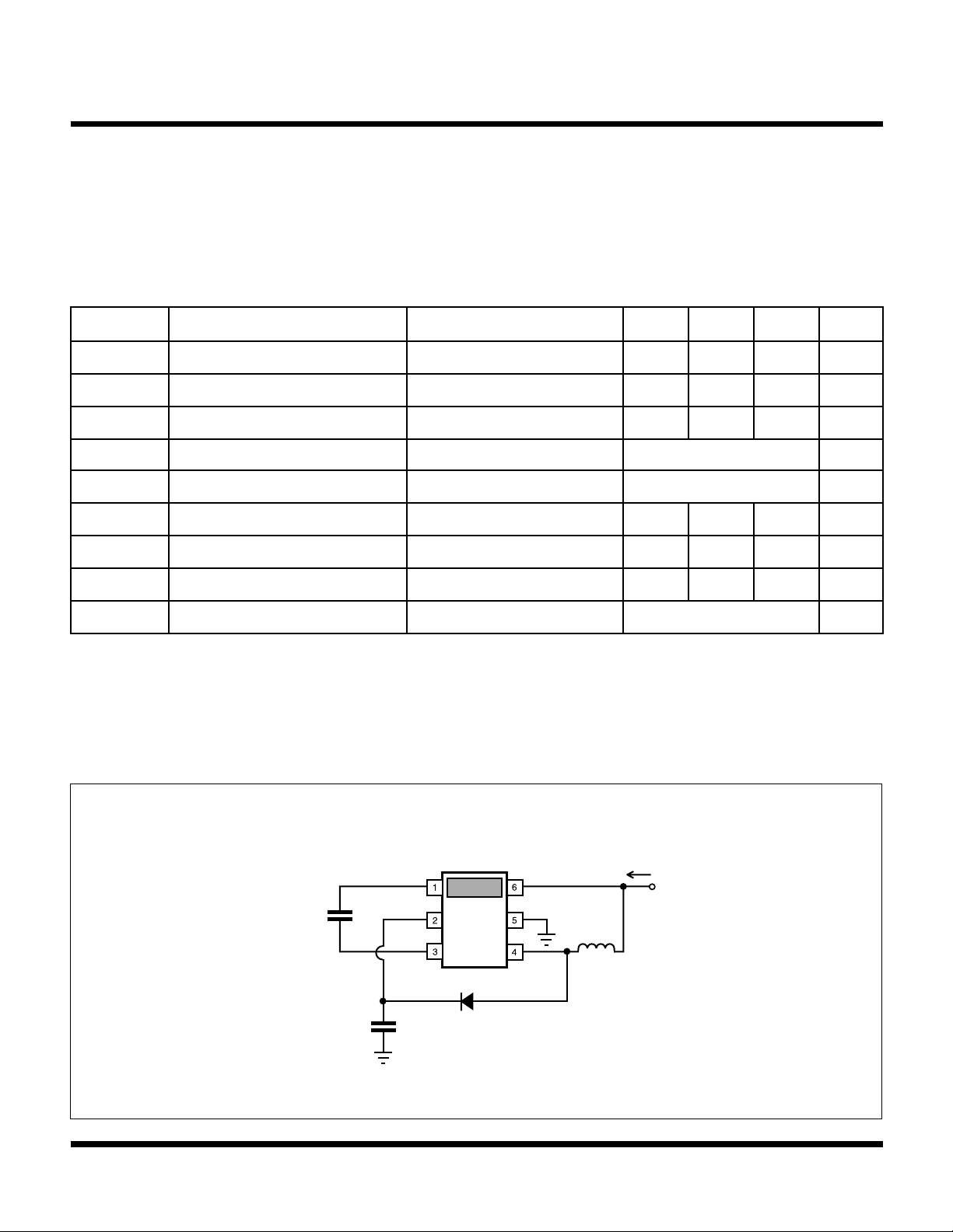
Note 3: When using test circuit below.
Gen. Note: Refer to “INDUCTOR VALUE SELECTION” and “INDUCTOR TYPE SELECTION” of Design Considerations Section for choosing
inductor.
Input Supply Range 2.7 3.6 6 V
Quiescent Current Current into pin 6 200 µA
Peak Current Threshold 44 52 60 mA
Lamp Frequency See Table 1 Hz
Boost Frequency See Table 2 kHz
Boost Clamp Voltage Force 100 µA into HV pin 90 105 120 V
Maximum Duty Cycle 88 92 96 %
Peak to Peak Lamp Voltage (Note 3) 125 140 155 V
Converter Supply Current (Notes 2, 3) See Table 3 mA
TEST CIRCUIT
I
L
1
680 µH
CONV
V
CC
C
EL
12 nF
+
EL
HV GND
-
EL
D
C
47 nF
1
1
V
CC
IND
Note: L1 = Toko Low Profile D52FU Series: 875FU-681 M
D1 = DIODES INC. DL4148
C1 = AVX 12061C473KAT2A
Page 2 May 2000 TOKO, Inc.
Page 3

TK6592x ELECTRICAL CHARACTERISTICS
VIN = 3.6 V, TA = Tj = 25 °C, unless otherwise specified.
TABLE 1: LAMP FREQUENCY
TOKO PART NO. MIN. TYP. MAX.
TK65920 157 Hz 175 Hz 193 Hz
TK65921 180 Hz 200 Hz 220 Hz
TK65922 202 Hz 225 Hz 248 Hz
TK65923 225 Hz 250 Hz 275 Hz
TK65924 247 Hz 275 Hz 303 Hz
TK65925 270 Hz 300 Hz 330 Hz
TK65926 292 Hz 325 Hz 358 Hz
TK65927 315 Hz 350 Hz 385 Hz
TK65928 337 Hz 375 Hz 413 Hz
TK65929 360 Hz 400 Hz 440 Hz
TABLE 2: OSCILLATOR FREQUENCY
TK6592x
TOKO PART NO. MIN. TYP. MAX.
TK65920 20.1 kHz 22.4 kHz 24.7 kHz
TK65921 23.0 kHz 25.6 kHz 28.2 kHz
TK65922 25.9 kHz 28.8 kHz 31.7 kHz
TK65923 28.8 kHz 32.0 kHz 35.2 kHz
TK65924 31.6 kHz 35.2 kHz 38.8 kHz
TK65925 34.5 kHz 38.4 kHz 42.3 kHz
TK65926 37.4 kHz 41.6 kHz 45.8 kHz
TK65927 40.3 kHz 44.8 kHz 49.3 kHz
TK65928 43.2 kHz 48.0 kHz 52.8 kHz
TK65929 46.1 kHz 51.2 kHz 56.3 kHz
TABLE 3: CONVERTER SUPPLY CURRENT
TOKO PART NO. MIN. TYP. MAX.
TK65920 - 7.8 mA 15.6 mA
TK65921 - 9.0 mA 18.0 mA
TK65922 - 10.1 mA 20.2 mA
TK65923 - 11.2 mA 22.4 mA
TK65924 - 12.3 mA 24.6 mA
TK65925 - 13.4 mA 26.8 mA
TK65926 - 14.5 mA 29.0 mA
TK65927 - 15.6 mA 31.2 mA
TK65928 - 16.8 mA 33.6 mA
TK65929 - 17.9 mA 35.8 mA
May 2000 TOKO, Inc. Page 3
Page 4
TK6592x
V
(V)
V
(V)
6
TYPICAL PERFORMANCE CHARACTERISTICS
USING TEST CIRCUIT
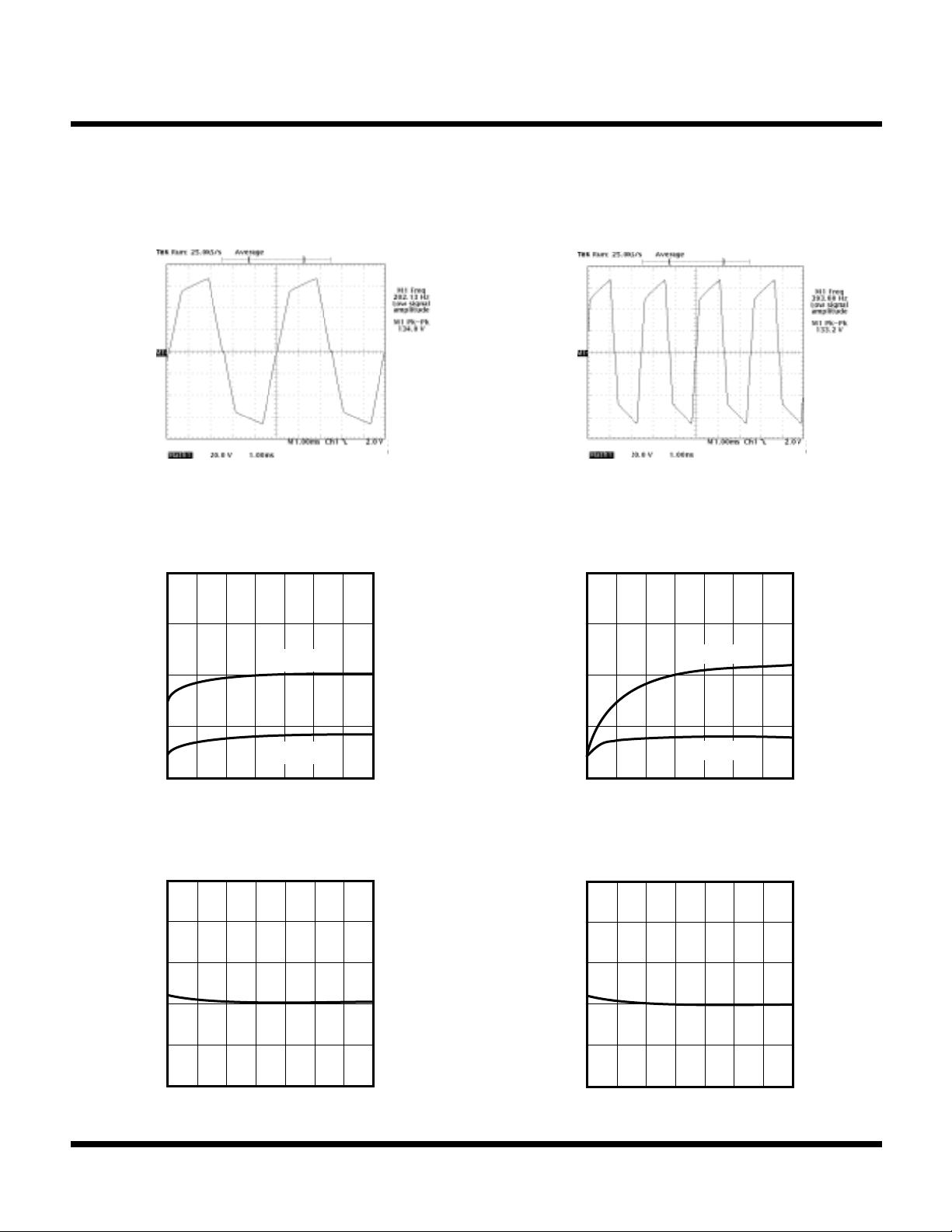
TK65929 Voltage Waveform Across 12 nF LampTK65921 Voltage Waveform Across 12 nF Lamp
PEAK TO PEAK LAMP VOLTAGE
160
150
140
OUT
130
120
2.5 3 3.5 4 4.5 5 5.5 6
230
220
210
(Hz)
TK65921
vs. SUPPLY VOLTAGE
L1 = 680 µH
L1 = 560 µH
VCC (V)
TK65921
LAMP FREQUENCY
vs. SUPPLY VOLTAGE
PEAK TO PEAK LAMP VOLTAGE
160
150
140
OUT
130
120
2.5 3 3.5 4 4.5 5 5.5 6
460
440
420
(Hz)
TK65929
vs. SUPPLY VOLTAGE
L1 = 680 µH
L1 = 560 µH
VCC (V)
TK65929
LAMP FREQUENCY
vs. SUPPLY VOLTAGE
200
LAMP
F
190
180
2.5 3 3.5 4 4.5 5 5.5
VCC (V)
400
LAMP
F
380
360
2.5 3 3.5 4 4.5 5 5.5 6
VCC (V)
Page 4 May 2000 TOKO, Inc.
Page 5
TYPICAL PERFORMANCE CHARACTERISTICS (CONT.)
6
USING TEST CIRCUIT
TK6592x
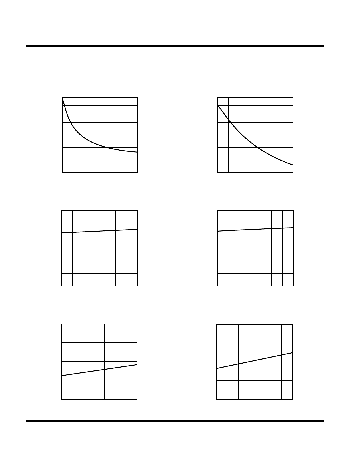
AVERAGE CONVERTER SUPPLY
CURRENT vs. SUPPLY VOLTAGE
18
16
14
12
(mA)
10
8
CONV
I
6
4
2
0
2.5 3 3.5 4 4.5 5 5.5
PEAK CURRENT THRESHOLD
60
55
50
(mA)
45
PEAK
I
40
TK65921
VCC (V)
TK65921
vs. SUPPLY VOLTAGE
AVERAGE CONVERTER SUPPLY
CURRENT vs. SUPPLY VOLTAGE
26
24
22
20
(mA)
18
16
CONV
I
14
12
10
8
2.5 3 3.5 4 4.5 5 5.5 6
PEAK CURRENT THRESHOLD
60
55
50
(mA)
45
PEAK
I
40
TK65929
VCC (V)
TK65929
vs. SUPPLY VOLTAGE
35
30
2.5 3 3.5 4 4.5 5 5.5 6
VCC (V)
TK65921
QUIESCENT CURRENT
vs. SUPPLY VOLTAGE
2.5 3 3.5 4 4.5 5 5.5 6
VCC (V)
(µA)
I
200
150
100
Q
50
0
35
30
2.5 3 3.5 4 4.5 5 5.5 6
VCC (V)
TK65929
QUIESCENT CURRENT
vs. SUPPLY VOLTAGE
0
2.5 3 3.5 4 4.5 5 5.5 6
VCC (V)
(µA)
I
200
150
100
Q
50
May 2000 TOKO, Inc. Page 5
Page 6
TK6592x
V
(V)
V
(V)
F
(H
)
F
(H
)
5
(°C)
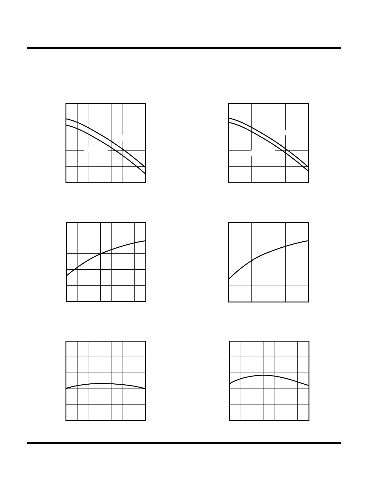
TYPICAL PERFORMANCE CHARACTERISTICS (CONT.)
USING TEST CIRCUIT
PEAK TO PEAK LAMP VOLTAGE
160
150
140
OUT
130
120
110
-50 -25 0 25 50 75 100 125
220
210
z
200
TK65921
vs. TEMPERATURE
VCC = 3.6 V
VCC = 2.7 V
TEMPERATURE (°C)
TK65921
LAMP FREQUENCY
vs. TEMPERATURE
PEAK TO PEAK VOLTAGE
160
150
140
OUT
130
120
110
-50 -25 0 25 50 75 100 125
440
420
z
400
TK65929
vs. TEMPERATURE
VCC = 3.6 V
VCC = 2.7 V
TEMPERATURE (°C)
TK65929
LAMP FREQUENCY
vs. TEMPERATURE
LAMP
190
180
170
-50 -25 0 25 50 75 100 125
TEMPERATURE (°C)
AVERAGE CONVERTER SUPPLY
CURRENT vs. TEMPERATURE
14
12
10
(mA)
CONV
8
I
6
4
-50 -25 0 25 50 75 100 12
TK65921
TEMPERATURE (°C)
LAMP
380
360
340
-50 -25 0 25 50 75 100 125
TEMPERATURE (°C)
AVERAGE CONVERTER SUPPLY
CURRENT vs. TEMPERATURE
22
20
18
(mA)
CONV
16
I
14
12
-50 -25 0 25 50 75 100 125
TK65929
TEMPERATURE
Page 6 May 2000 TOKO, Inc.
Page 7
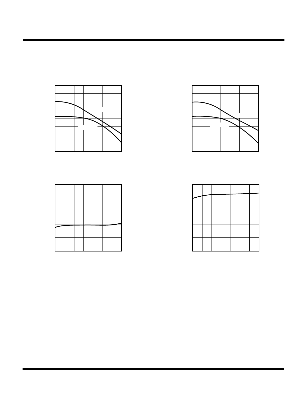
TYPICAL PERFORMANCE CHARACTERISTICS (CONT.)
I
(
A)
I
(
A)
I
(
A)
I
(
A)
USING TEST CIRCUIT
TK6592x
PEAK CURRENT THRESHOLD
58
56
54
52
m
50
PEAK
48
46
44
42
-50 -25 0 25 50 75 100 125
100
90
80
µ
Q
70
TK65921
vs. TEMPERATURE
VCC = 3.6 V
VCC = 2.7 V
TEMPERATURE (°C)
TK65921
QUIESCENT CURRENT
vs. TEMPERATURE
PEAK CURRENT THRESHOLD
58
56
54
52
m
50
PEAK
48
46
44
42
-50 -25 0 25 50 75 100 125
100
90
80
µ
Q
70
TK65929
vs. TEMPERATURE
VCC = 2.7 V
TEMPERATURE (°C)
TK65929
QUIESCENT CURRENT
vs. TEMPERATURE
VCC = 3.6 V
60
50
-50 -25 0 25 50 75 100 125
TEMPERATURE (°C)
60
50
-50 -25 0 25 50 75 100 125
TEMPERATURE (°C)
May 2000 TOKO, Inc. Page 7
Page 8
TK6592x
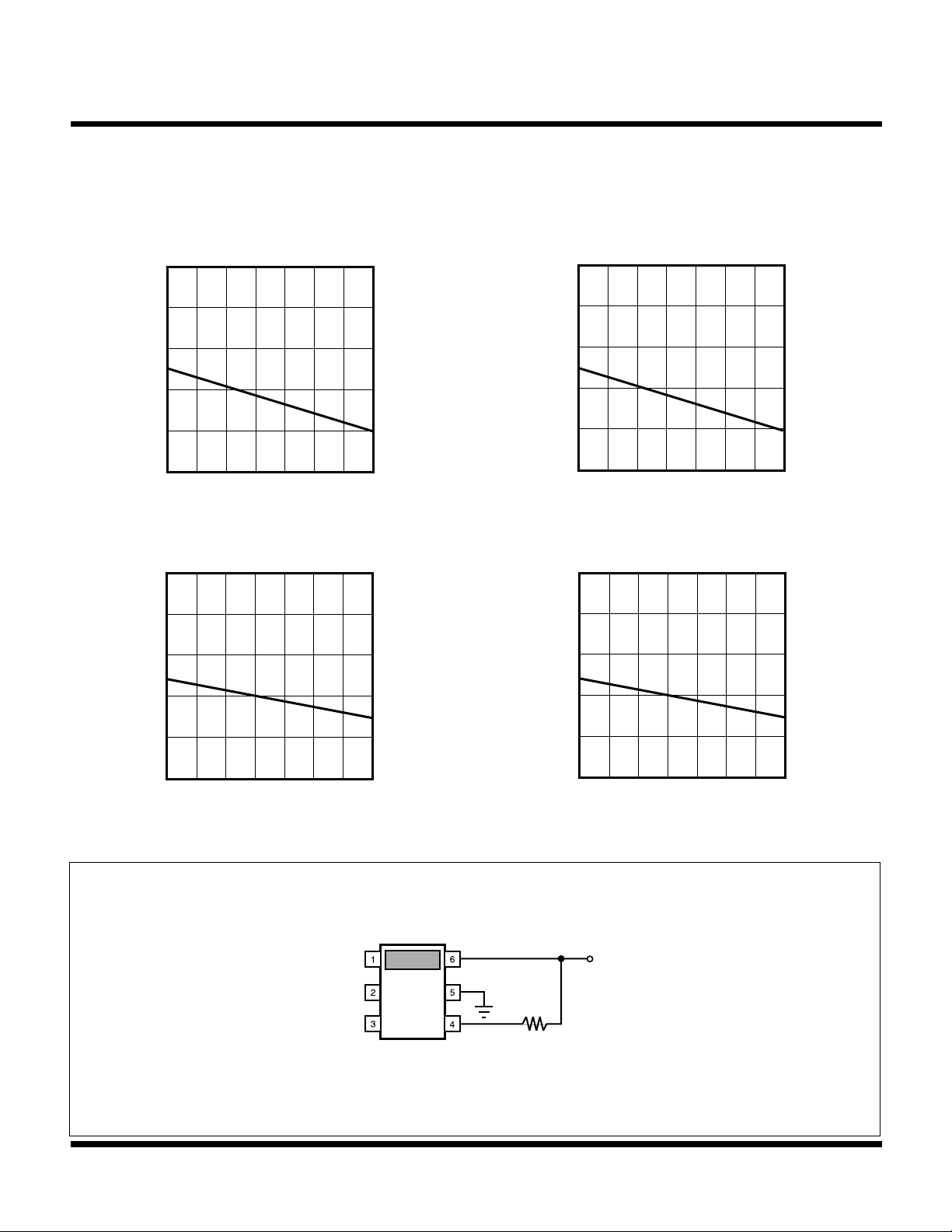
TYPICAL PERFORMANCE CHARACTERISTICS (CONT.)
USING D
TEST CIRCUIT
(MAX)
TK65921
MAXIMUM DUTY CYCLE
95
94
(%)
93
(MAX)
D
92
91
90
95
94
(%)
93
vs. SUPPLY VOLTAGE
2.5 3 3.5 4 4.5 5 5.5 6
VCC (V)
TK65921
MAXIMUM DUTY CYCLE
vs. TEMPERATURE
MAXIMUM DUTY CYCLE
95
94
(%)
93
(MAX)
D
92
91
90
2.5 3 3.5 4 4.5 5 5.5 6
95
94
(%)
93
TK65929
vs. SUPPLY VOLTAGE
VCC (V)
TK65929
MAXIMUM DUTY CYCLE
vs. TEMPERATURE
(MAX)
D
92
91
90
-50 -25 0 25 50 75 100 125
TEMPERATURE (°C)
D
+
EL
HV GND
-
EL
TEST CIRCUIT
(MAX)
V
IND
CC
(MAX)
D
92
91
90
-50 -25 0 25 50 75 100 125
TEMPERATURE (°C)
V
CC
R
1
Note: R1 = 470 Ω
Page 8 May 2000 TOKO, Inc.
Page 9
THEORY OF OPERATION
TK6592x
An Electroluminescent (EL) Lamp is a strip of plastic,
coated with a phosphorous material that emits light when
a high voltage AC signal is applied to the terminals of the
device. EL panels have the ability to light the entire panel
uniformly. Because of this, they are gradually becoming
more popular and widespread than LEDs. The amount of
light emitted from an EL Lamp is typically proportional to
the magnitude of the voltage applied to the lamp.
Furthermore, the color of the light emitted by an EL Lamp
is somewhat dependent upon the frequency of the applied
drive signal. For most applications, a peak-to-peak voltage
of 100 to 170 V, with a drive frequency of 175 to 400 Hz,
provides optimal trade-off between lamp intensity and
power consumption.
The capacitance of the EL Panel is typically proportional to
the size of the lamp (a 1 square inch EL Panel typically
exhibits approximately 5 nF of capacitance load). The
TK6592x series of devices has been optimized to drive EL
panels, which are approximately 2-4 square inches in size.
The Boost section of the TK6592x consists of a controller
for stepping up a relatively low voltage (2.7 to 6 V) to a
much higher voltage (50 to 90 V) needed to drive the EL
Lamp. The boost section of the TK6592x uses a proprietary
architecture which provides a relatively constant output
power, independent of the input supply, without the need
for sensing the high voltage output of the boost converter.
By controlling the peak current through the switching
element of the boost converter, the boost section provides
a constant output power independent of the input supply.
The H-Bridge section of the TK6592x switches the high
voltage output of the boost converter to the two terminals
of the EL Lamp. By alternately switching the terminals of
the lamp between the high voltage supply and ground, the
peak-to-peak voltage developed across the lamp is
effectively twice the high voltage generated by boost
converter. Furthermore, the TK6592x limits the magnitude
of the drive currents through the H-Bridge switches in
order to minimize the edge rates developed across the EL
Lamp. This approach protects the EL Panel from large
current spikes and reduces the likelihood of high frequency
noise components being injected into neighboring circuitry.
The Oscillator section of the TK6592x generates a fixed
frequency clock source for the previously described Boost
and H-Bridge sections, without the need for external
components. The high frequency output of the oscillator is
used for driving the boost controller. A lower frequency
clock is generated by dividing the high frequency clock by
128; this lower frequency clock corresponds to the drive
frequency of the EL Lamp. The laser-trimmed oscillators
are relatively insensitive to variations in temperature and
supply voltage. Therefore, they provide good control of the
lamp color emitted by the panel.
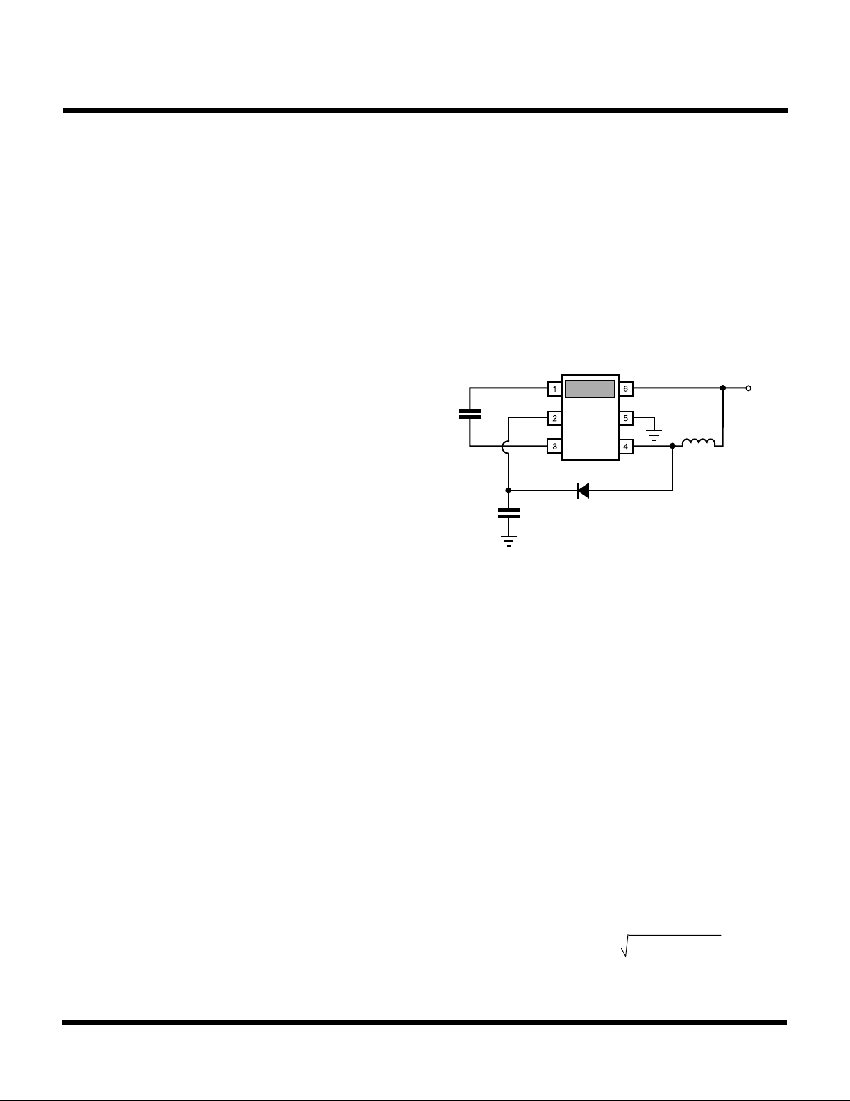
The circuit below illustrates a typical application where the
TK6592x is driving a 2-square-inch EL Lamp with a
capacitance of approximately 12 nF.
C
EL
12 nF
+
EL
HV GND
-
EL
D
C
47 nF
1
1
V
IND
CC
V
IN
L
1
FIGURE 1: TYPICAL APPLICATION
By keeping the ratio of the boost frequency and the HBridge frequency constant, the peak-to-peak output voltage
from the TK6592x becomes primarily dependent upon the
capacitance of the EL Lamp, the peak current threshold of
the boost converter, and the value of the inductive element
used in the boost converter. For the TK6592x, the peak
current threshold is laser-trimmed to 52 mA. The capacitive
load of the EL Lamp is a function of panel size and is
typically fixed. Therefore, the high voltage output of the
boost converter can be set to a desired voltage by selecting
the appropriate value of the inductive element used in the
boost converter.
I
= Boost Peak Current Threshold (52 mA)
PEAK
C
= Capacitance of EL Lamp
EL
L = Inductance Value
VHV = (I
/ 2) x (L /CEL) x 128
PEAK
May 2000 TOKO, Inc. Page 9
Page 10
TK6592x
HV
HVP HVP
UL UR
EL Panel
LL LR
Current Source 1
Current Source 2
EL
-
EL
+
THEORY OF OPERATION (CONT.)
With properly selected components, the TK6592x will
nominally support peak output voltages to 90 V
(180 V
from the driver outputs, the removal of the load can cause
the output voltage to increase beyond 90 V. To protect
against this fault condition, a clamp circuit exists on the
high voltage output which nominally limits the output
voltage to a typical value of 105 V (210 V
H-BRIDGE SECTION OPERATION
). Should the EL Panel become disconnected
PK-PK
).
PK-PK
DETAILS CONCERNING THE
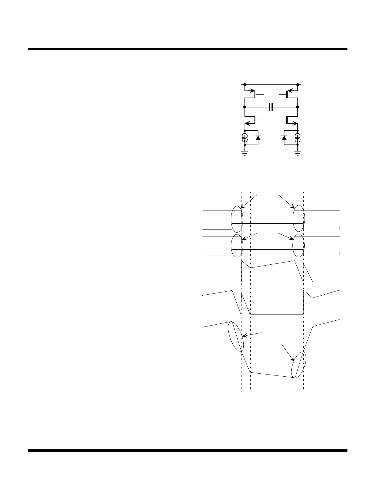
In an effort to extend EL lamp life, reduce EMI emissions,
and reduce the power draw of the IC, current sources to
control the charging and discharging of the EL lamp panel
and special sequencing control of the H-bridge FETs were
added to the H-bridge of TK659xx.
Current sources were added between ground and the
sources of the low-side N-channel FETs (Figure 2).
Therefore, the current into and out of the EL panel is
controlled and limited.
The FETs are turned off and on in the sequence shown in
Figure 3. As is noted in Figure 3, there is a period of time
when both of lower N-channel FETs are turned on and both
of upper P-channel FETs are turned off. This provides a
period of time to discharge the EL panel capacitance
completely; before starting to recharge it again with current
from HV voltage rail. Therefore, this special sequencing
method prevents taking current off the HV voltage rail
during the discharge of EL panel capacitance and operates
more efficiently.
FIGURE 2: H-BRIDGE SCHEMATIC
BOTH OFF
UL
UR
LL
LR
V
V
EL
EL
OFF
OFF
ON
ON
-
+
ON
OFF
BOTH ON
OFF
ON
Discharging
EL Panel
Capacitance
OFF
OFF
ON
ON
OFF
ON
ON
OFF
Page 10 May 2000 TOKO, Inc.
+
-
V
-
EL
V
=
V
EL
EL
FIGURE 3: H-BRIDGE SEQUENCING WAVEFORMS
Page 11

TK6592x
PIN DESCRIPTIONS
SUPPLY PIN (VCC)
This pin is the positive input supply for the TK6592x. Good design practices dictate capacitive decoupling to the ground
pin.
GROUND PIN (GND)
The pin provides the ground connection for the IC.
IND PIN
This pin is periodically pulled to ground by a power transistor acting as an internal switch to the TK6592x. Externally, this
pin is typically connected to an inductor and a rectifying diode. By modulating the switching action of the internal switch,
the TK6592x can boost the relatively low voltage of the battery to the high voltage required to drive the EL Lamp.
HV PIN
This pin is connected to the filter capacitor and the cathode of the rectifying diode in order to generate a high voltage
supply. This high voltage supply is switched to the terminals of the EL Lamp through the H-Bridge.
+
EL
PIN
This pin is connected to one side of the EL Panel.
EL- PIN
This pin is connected to the other side of the EL Panel.
Note: Measuring the voltage across the EL lamp (EL+ pin to EL- pin) should be done with balanced scope probes using
differential measurement techniques to obtain a true waveform of the voltage across the EL lamp.
May 2000 TOKO, Inc. Page 11
Page 12
TK6592x
DESIGN CONSIDERATIONS
INDUCTOR VALUE SELECTION
Designing an EL Driver utilizing the TK6592x is a very simple task. The primary component affecting the behavior of the
converter is the inductor. Essentially, the entire design task primarily consists of selecting the proper inductor value and
type given the operating conditions of the EL Panel (e.g., lamp capacitance, frequency, output voltage, supply range).
The following tables and charts are intended to simplify the selection of the inductor.
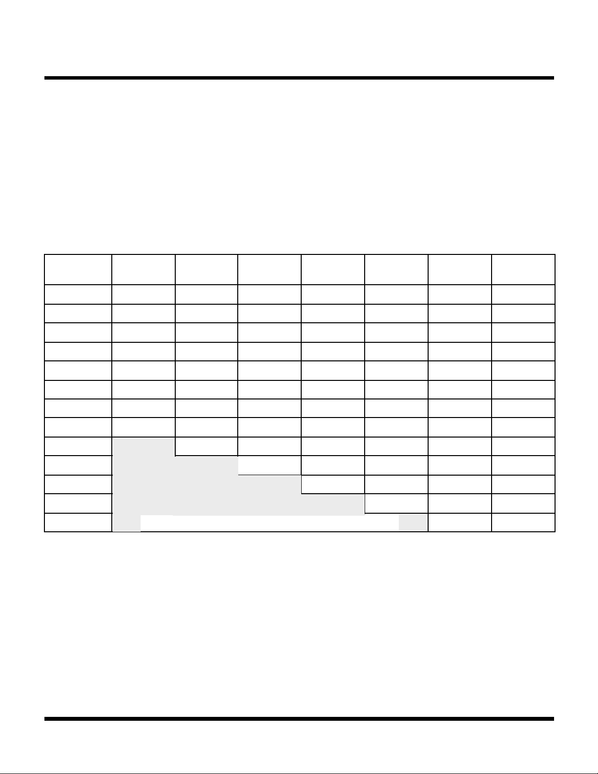
Given the capacitance of the EL Lamp, and the peak output voltage requirements, the following table can be utilized to
select the value of the inductive component.
TABLE 4: PEAK OUTPUT VOLTAGE VS. INDUCTOR VALUE AND LAMP CAPACITANCE
INDUCTOR
VALUE
180 µH 42 V 36 V 32 V 29 V 27 V 25 V 24 V
220 µH 46 V 40 V 36 V 33 V 30 V 28 V 27 V
330 µH 56 V 49 V 44 V 40 V 37 V 34 V 33 V
390 µH 61 V 53 V 47 V 43 V 40 V 37 V 35 V
470 µH 67 V 58 V 52 V 48 V 44 V 41 V 39 V
560 µH 73 V 64 V 57 V 52 V 48 V 45 V 42 V
680 µH 81 V 70 V 63 V 57 V 53 V 50 V 47 V
820 µH 89 V 77 V 69 V 63 V 58 V 54 V 51 V
1000 µH 85 V 76 V 69 V 64 V 60 V 57 V
1200 µH 83 V 76 V 70 V 66 V 62 V
1500 µH 85 V 79 V 74 V 69 V
1800 µH 86 V 81 V 76 V
2200 µH 89 V 84 V
Note: The voltages indicated in the table above may not be achievable under certain circumstances (i.e., low battery or higher drive frequencies).
Refer to the charts on page 12 to determine which output voltage/coil combination can be supported by the EL driver.
9.0 nF
LAMP
Close to 100 V operation check capacitor C1 voltage rating
12.0 nF
LAMP
15.0 nF
LAMP
18.0 nF
LAMP
21.0 nF
LAMP
24.0 nF
LAMP
27.0 nF
LAMP
As an example as to how the above table is to be used, assume that we have a 2-square-inch panel (12 nF capacitance)
and we would like the peak-to-peak voltage across the lamp to be 140 V. The peak voltage on either terminal would be
70 V (140 V / 2). Referring to the table above, we can see that using a 680 µH coil the peak voltage developed across
a 12 nF Lamp would be approximately 70 V. In this particular example, the inductive component should have a value of
680 µH.
INDUCTOR TYPE SELECTION
After the value of the inductor has been selected, an appropriate coil type needs to be selected taking into account such
factors as DC resistance and current capability. The following charts can be utilized for selecting the proper family of Toko
Coils. Furthermore, the following charts will also indicate if the TK6592x is the appropriate driver given the frequency and
input supply requirements. If the TK6592x does not have sufficient drive capability given the input supply and frequency
Page 12 May 2000 TOKO, Inc.
Page 13
TK6592x
INDUCTOR
VALUE
(
H)
INDUCTOR
VALUE
(
H)
INDUCTOR
VALUE
(
H)
INDUCTOR
VALUE
(
H)
INDUCTOR
VALUE
(
H)
DESIGN CONSIDERATIONS (CONT.)
requirements, the following charts will suggest the TK6593x family of EL Drivers which have higher drive capabilities.
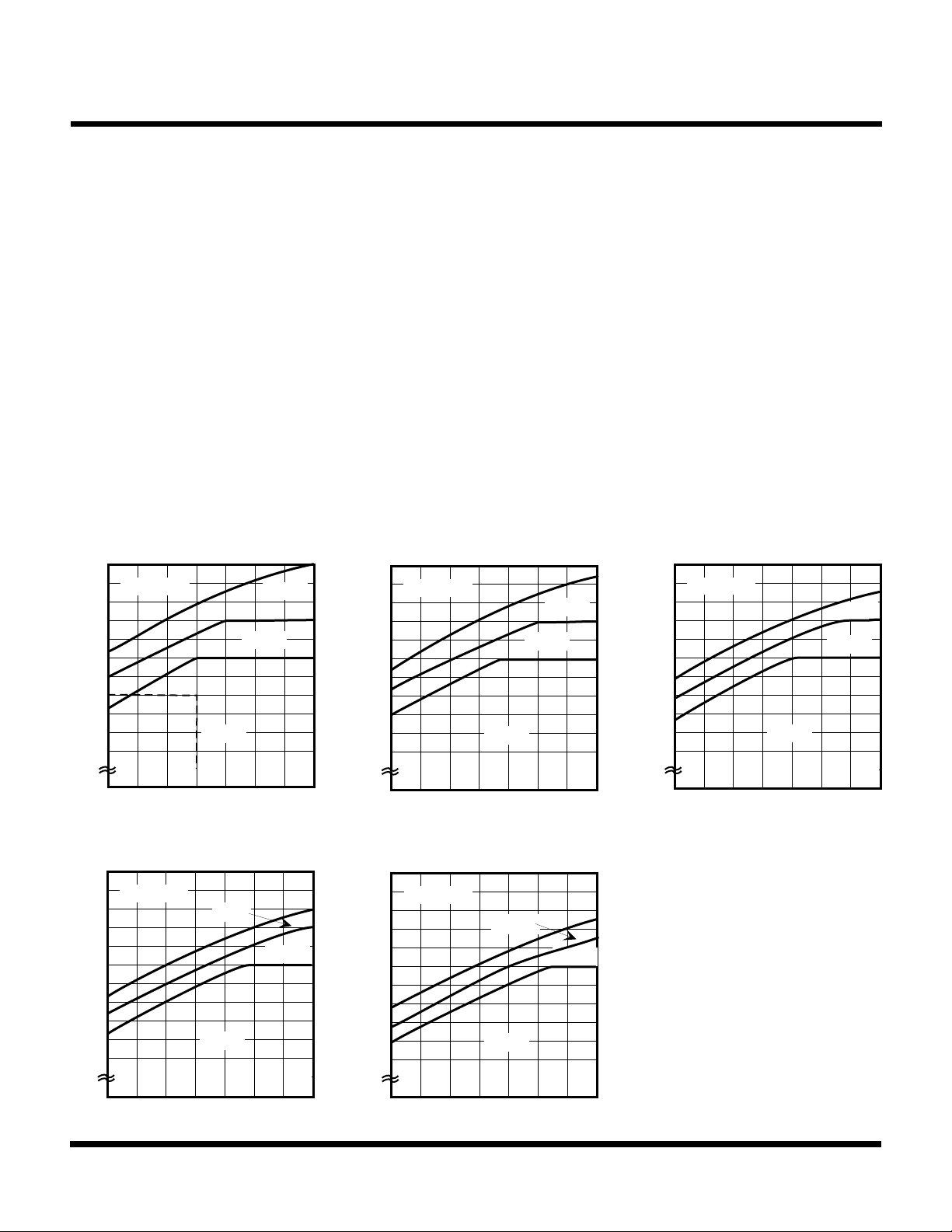
To utilize the following charts in selecting an appropriate coil, perform the following steps:
1) From the following charts, select the chart that matches the part number of the Toko EL Driver that will be used in
the application. The part number of the Toko EL Driver will be dependant upon the desired frequency of the EL panel
(e.g., TK65921 = 200Hz).
2) Determine input supply voltage range (e.g., 4 to 6 V). The x-axis of the following charts represent the minimum
expected supply voltage. Below this minimum supply voltage the EL Driver output may begin to droop. On the
appropriate chart, draw a vertical line upward from the minimum supply voltage represented on the x-axis (e.g., 4V).
3) Draw a horizontal line passing through the chosen inductor value on the y-axis (e.g., 680 µH).
4) The vertical and horizontal lines drawn in steps 2 and 3 respectively will intersect at a point. This point will lie in one
of four regions of the chart (e.g., D31FU). These four regions suggest which family of Toko Coils to use.
Of the three coil families suggested in these charts, the D31FU has the smallest physical size but also has higher DC
resistance. The D52FU series of coils has the largest physical size and the lowest DC resistance. The D52FU or the
D32FU can be used as a reasonable substitute for the D31FU. Similarly, the D52FU can be used as a replacement for
the D32FU. Substituting a coil with lower DC resistance will generally result in a system that will consume less power
supply current.
2200
1800
µ
1500
1200
1000
2200
1800
µ
1500
1200
1000
820
680
560
470
390
180
820
680
560
470
390
TK65920, TK65921
USE TK6593X
X
D31FU
3 4 5 6
MINIMUM SUPPLY (V)
TK65926, TK65927
USE TK6593X
D31FU
D52FU
D32FU
D52FU
D32FU
2200
1800
µ
1500
1200
1000
2200
1800
µ
1500
1200
1000
820
680
560
470
390
180
820
680
560
470
390
TK65922, TK65923
USE TK6593X
D52FU
D32FU
D31FU
3 4 5 6
MINIMUM SUPPLY (V)
TK65928, TK65929
USE TK6593X
D52FU
D32FU
D31FU
2200
1800
µ
1500
1200
1000
820
680
560
470
390
180
TK65924, TK65925
USE TK6593X
D52FU
D32FU
D31FU
3 4 5 6
MINIMUM SUPPLY (V)
180
3 4 5 6
MINIMUM SUPPLY (V)
180
3 4 5 6
MINIMUM SUPPLY (V)
May 2000 TOKO, Inc. Page 13
Page 14
TK6592x
SPLIT SUPPLY APPLICATION
APPLICATION INFORMATION
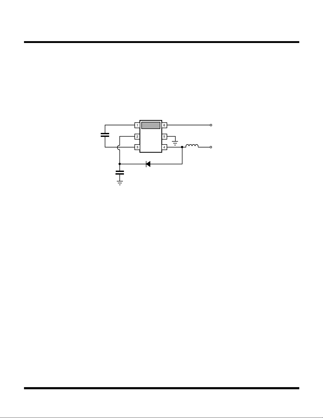
The split power supply application of this EL driver IC is a circuit configuration (see Figure 4) in which the V
(V
) is separated or split away from the main power input (V
control
+
EL
C
5 nF
EL
HV GND
-
EL
C
22 nF
D
1
) supplying current to the inductor.
power
V
CC
IND
L
1
1
V
control
from
2.7 to 6 V
max. 200 µA
V
power
from
0.9 to 20 V
FIGURE 4: SPLIT SUPPLY APPLICATION CIRCUIT
IC power
CC
The voltage supplied to the VCC pin of the IC (V
draw on this power supply rail of the system would be very small (under 200 µA). This V
off the EL lamp driver, which permits the V
power
) needs to be maintained in the 2.7 V to 6.0 V range, but the current
control
can be used to turn on and
control
to be connected to the battery or other power source directly with the
least amount of resistance in the power path as possible.
Now with the VCC power for the IC (V
) being supplied from a different source, the main power (V
control
) can be any
power
voltage between 0.9 V and 20 V. But it is critical to properly select the inductor such that the proper peak current
regulation is maintained over the input voltage operating range of the converter.
If the inductor value is too large the current will rise too slowly and not have time to reach its set peak current trip point
at low input voltages, but at high input voltage the current might rise too quickly and overshoot the set peak current trip
point.
The primary battery applications for this part are in a dual cell alkaline or dual cell Li-Ion system (such as a GPS or smart
cell phones). These systems are assumed to have a minimum useable input voltage of 1.8 V for the dual cell alkaline
system and 5.4 V for the dual cell Li-Ion system.
For low converter input voltages (1.8 V and 5.4 V minimum input voltages), Table 5 shows the recommended maximum
inductance value for a given device part number (therefore a given frequency of operation) and a minimum input voltage.
Each cell in the table gives three inductance values; each value (in µH) corresponds to each type of specialized Toko
EL driver inductors (D31FU, D32FU, and D52FU types of Toko inductors).
Page 14 May 2000 TOKO, Inc.
Page 15
APPLICATION INFORMATION (CONT.)
TABLE 5: DUAL CELL ALKALINE AND DUAL CELL LI-ION INDUCTANCE SELECTION TABLE
TK6592x
PART NO.
f lamp
f converter
min.Vp L type
D31FU
1.8V D32FU
D52FU
D31FU
5.4V D32FU
D52FU
TK65920
175 Hz
22.4 kHz
390 µH
560 µH
680 µH
1000 µH
1200 µH
2700 µH
TK65921
200 Hz
25.6 kHz
390 µH
560 µH
680 µH
1000 µH
1200 µH
2200 µH
TK65922
225 Hz
28.8 kHz
390 µH
470 µH
560 µH
1000 µH
1200 µH
2200 µH
TK65923
250 Hz
32.0 kHz
390 µH
470 µH
560 µH
1000 µH
1200 µH
1800 µH
TK65924
275 Hz
35.2 kHz
390 µH
470 µH
560 µH
1000 µH
1200 µH
1800 µH
TK65925
300 Hz
38.4 kHz
390 µH
470 µH
470 µH
1000 µH
1200 µH
1800 µH
TK65926
325 Hz
41.6 kHz
390 µH
390 µH
470 µH
1000 µH
1200 µH
1500 µH
TK65927
350 Hz
44.8 kHz
330 µH
390 µH
470 µH
1000 µH
1200 µH
1500 µH
TK65928
375 Hz
48.0 kHz
330 µH
390 µH
390 µH
1000 µH
1200 µH
1500 µH
TK65929
400 Hz
51.2 kHz
330 µH
330 µH
390 µH
1000 µH
1200 µH
1200 µH
After selecting the inductor type and value, Table 4 of the TK6592X data sheet can be used to determine the typical output
voltage for a given loading of EL lamp capacitance. If you wish to reduce this output voltage, just reduce the inductor’s
inductance value.
NOISE CONSIDERATIONS
There are two specific noise types relevant to the user when it comes to choosing EL Drivers: the Audio Noise and the
Electromagnetic Interference (EMI) Noise.
The EMI Noise would most likely come from the boost converter/coil section. The Toko EL Driver has specifically been
designed to address this issue.
The device runs at a fixed frequency and the frequency is controlled tightly in order to avoid interference.
Furthermore, the panel frequency is forced to be a 128 submultiple of the boost frequency avoiding any type of beating
frequencies.
By choosing shielded coils, the EMI noise problem can further be reduced.
The Audio Noise can come from several components which make up the system.
The coil, if operated in the audio range would be a source of noise. The Toko EL Driver was carefully designed to give
the user the choice of 10 frequencies such that the coil frequency will always be above audio range. Since the device
operates at a fixed frequency in discontinuous conduction mode, there are no possible submultiples which would cause
audible noise.
The filter capacitor can be a source of audio noise. Furthermore, depending on how this cap is mounted, the mounting
can act as an amplifier (as a speaker box). Certain ceramic caps driven from a high voltage source as in the EL Driver
case, demonstrate a PIEZOELECTRIC effect which is distinguishable in the Audio Range.
Other types of caps, such as film type do not denote an audio noise.
The panel itself, being operated well into the Audio Range (175 Hz to 400 Hz) and of a capacitive nature driven from high
voltage may also display Audible Noise. Mounting of this panel can enhance or diminish this natural effect of the panel.
May 2000 TOKO, Inc. Page 15
Page 16
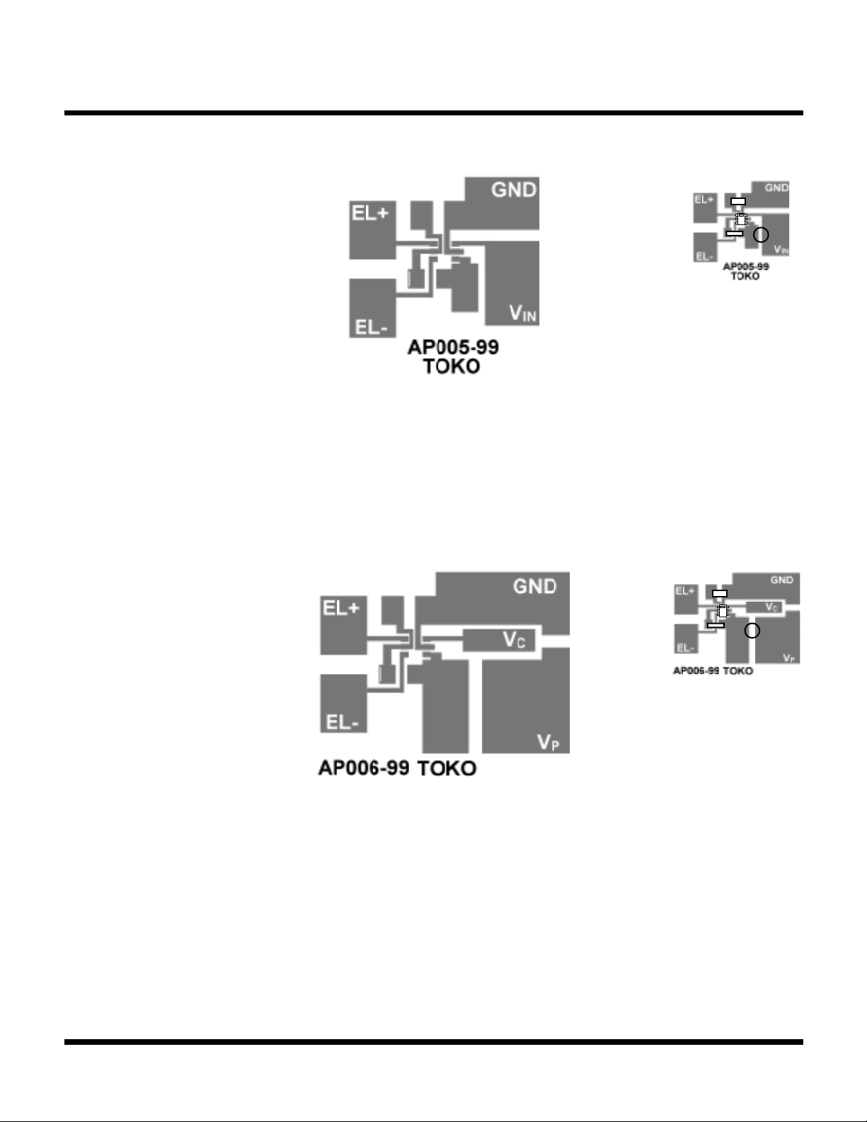
TK6592x
LAYOUT
Actual Size
2x
SPLIT SUPPLY LAYOUT
2x
Actual Size
Page 16 May 2000 TOKO, Inc.
Page 17

NOTES
TK6592x
May 2000 TOKO, Inc. Page 17
Page 18

TK6592x
NOTES
Page 18 May 2000 TOKO, Inc.
Page 19

NOTES
TK6592x
May 2000 TOKO, Inc. Page 19
Page 20
TK6592x
(
)
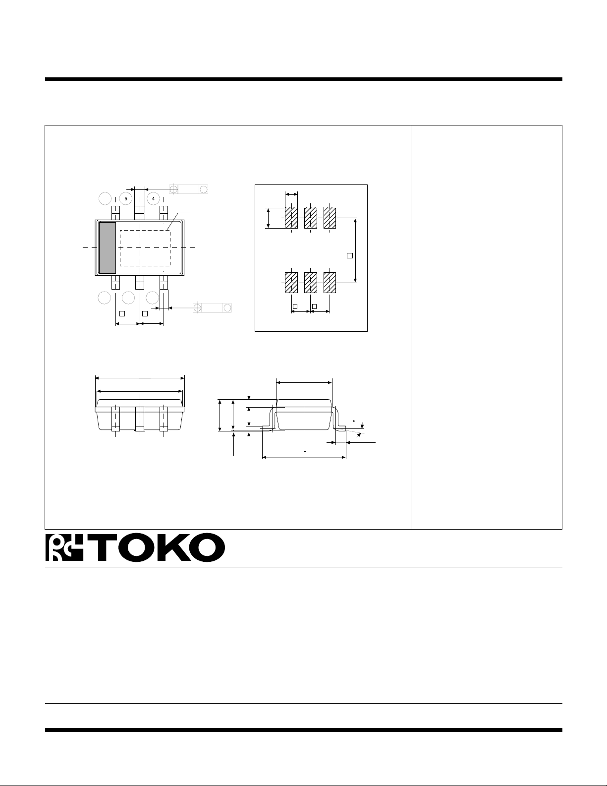
PACKAGE OUTLINE
SOT23L-6
Dimensions are shown in millimeters
Tolerance: x.x = ± 0.2 mm
+0.15
0.4
- 0.05
6
123
e
e
0.95
0.95
+0.3
- 0.1
3.5
(3.4)
unless otherwise specified
0.32
5 PL
Marking Information
Marking
TK65920 B0
0.1
+0.15
- 0.05
M
Marking
0.1
M
0.3
1.2
1.4 max
+0.15
- 0.05
0 - 0.1
0.15
0.6
1.0
e
Recommended Mount Pad
3.3
0.95
3.0
e1
e
0.95
2.2
15 max
+ 0.3
0.4
TK65921 B1
TK65922 B2
TK65923 B3
TK65924 B4
TK65925 B5
TK65926 B6
TK65927 B7
TK65928 B8
TK65929 B9
Toko America, Inc. Headquarters
1250 Feehanville Drive, Mount Prospect, Illinois 60056
Tel: (847) 297-0070 Fax: (847) 699-7864
TOKO AMERICA REGIONAL OFFICES
Midwest Regional Office
Toko America, Inc.
1250 Feehanville Drive
Mount Prospect, IL 60056
Tel: (847) 297-0070
Fax: (847) 699-7864
Western Regional Office
Toko America, Inc.
2480 North First Street , Suite 260
San Jose, CA 95131
Tel: (408) 432-8281
Fax: (408) 943-9790
Eastern Regional Office
Toko America, Inc.
107 Mill Plain Road
Danbury, CT 06811
Tel: (203) 748-6871
Fax: (203) 797-1223
Semiconductor Technical Support
Toko Design Center
4755 Forge Road
Colorado Springs, CO 80907
Tel: (719) 528-2200
Fax: (719) 528-2375
Visit our Internet site at http://www.tokoam.com
The information furnished by TOKO, Inc. is believed to be accurate and reliable. However, TOKO reserves the right to make changes or improvements in the design, specification or manufacture of its
products without further notice. TOKO does not assume any liability arising from the application or use of any product or circuit described herein, nor for any infringements of patents or other rights of
third parties which may result from the use of its products. No license is granted by implication or otherwise under any patent or patent rights of TOKO, Inc.
Page 20 May 2000 TOKO, Inc.
All Rights Reserved
IC-xxx-TK6592x
0798O0.0K
Printed in the USA© 1999 Toko, Inc.
 Loading...