

Page 1
ADVANCED INFORMATION
V
IN
GND
SW
LOI
V
OUT
CONTROL
CIRCUIT
OSCILLATOR
Vref UVLO
LBI
20P
ADVANCED INFORMATION
TK652xx
STEP-UP VOLTAGE CONVERTER WITH VOLTAGE MONITOR
FEATURES
■ Guaranteed 0.9 V Operation
■ Very Low Quiescent Current
■ Internal Bandgap Reference
■ High Efficiency MOS Switching
■ Low Output Ripple
■ Laser-Trimmed Output Voltage
■ Low Output Voltage Monitor
■ Low Battery Monitor
■ Undervoltage Lockout
■ Regulation by Pulse Burst Modulation (PBM)
DESCRIPTION
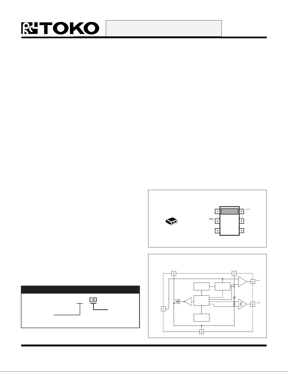
The TK652xx low power step-up DC-DC converter is
designed for portable battery powered systems, capable
of operating from a single battery cell down to 0.9 V. The
TK652xx provides the power switch and the control circuit
for a boost converter. The converter takes a DC input and
boosts it up to a regulated 1.8, 2.1, or 2.4 V.
The output voltage is laser-trimmed. Two internal detectors
monitor the output voltage and battery voltage. The Low
Output Indicator (LOI) generates an active low when the
battery voltage falls below 90 % of the output voltage. The
Low Battery Indicator (LBI) generates an active low when
the battery voltage falls below 1.1 V. These outputs can be
used to notify the microprocessor or power monitor circuit
of a fault condition. An internal Undervoltage Lockout
(UVLO) circuit is utilized to prevent the inductor switch
from remaining in the “on” mode when the battery voltage
is too low to permit normal operation. Pulse Burst
Modulation (PBM) is used to regulate the voltage at the
V
pin of the IC. PBM is the process in which an
OUT
oscillator signal is gated or not gated to the switch drive
each period. The decision is made just before the start of
each cycle and is based on comparing the output voltage
to an internally-generated bandgap reference. The decision
APPLICATIONS
■ Battery Powered Systems
■ Cellular Telephones
■ Pagers
■ Personal Communications Equipment
■ Portable Instrumentation
■ Portable Consumer Equipment
■ Radio Control Systems
is latched, so the duty ratio is not modulated within a cycle.
The average duty ratio is effectively modulated by the
“bursting” and skipping of pulses which can be seen at the
SW pin of the IC. Special care has been taken to achieve
high reliability through the use of Oxide, double Nitride
passivation. The TK652xx is available in a miniature
SOT-23L-6 surface mount package.
Customized levels of accuracy in oscillator frequency and
output voltage are available.
TK652xx
V
IN
LBI
SW
BLOCK DIAGRAM
LOI
GND
V
OUT
ORDERING INFORMATION
Voltage Code
VOLTAGE CODE
18 = 1.8 V
21 = 2.1 V
24 = 2.4 V
January 1999 TOKO, Inc. Page 1
TK652xxM
Tape/Reel Code
TAPE/REEL CODE
TL: Tape Left
Page 2
TK652xx
ADVANCED INFORMATION
ABSOLUTE MAXIMUM RATINGS
All Pins Except SW and GND .................................... 6 V
SW Pin ....................................................................... 9 V
Power Dissipation (Note 1) ................................ 400 mW
Storage Temperature Range ................... -55 to +150 °C
Operating Temperature Range ...................-20 to +80 °C
Junction Temperature ...........................................150 °C
TK652xx ELECTRICAL CHARACTERISTICS
Over operating temperature range and supply voltage range, unless otherwise specified.
LOBMYSRETEMARAPSNOITIDNOCTSETNIMPYTXAMSTINU
V
NI
f
CSO
V
∆V
∆V
D
V
Note 1: Derate at 0.8 mW/oC for operation above TA = 25 oC ambient temperature, when heat conducting copper foil path is maximized on the printed
)GER(TUO
)DAOL(TUO
)ENIL(TUO
CSO
IBL
circuit board. When this is not possible, a derating factor of 1.6 mW/ °C must be used.
egatloVylppuS09.006.1V
ycneuqerFrotallicsOlanretnIT
VfodlohserhTnoitalugeR
TUO
VfonoitalugeRdaoL
VfonoitalugeReniL
)GER(TUO
)GER(TUO
A
T
A
V
NI
∆V
rotallicsOfooitaRytuDemit-nOT
A
dlohserhTrotacidnIyrettaBwoLT
A
C°52=273869zHk
C°52=%3-V
,V3.1=I
TUO
NI
I,V07.0=
TUO
Am4ot0=005Vm
Am1=
02-002Vm
TUO
%3+V
C°52=448445%
I,C°52=
TUO
Am1=50.101.151.1V
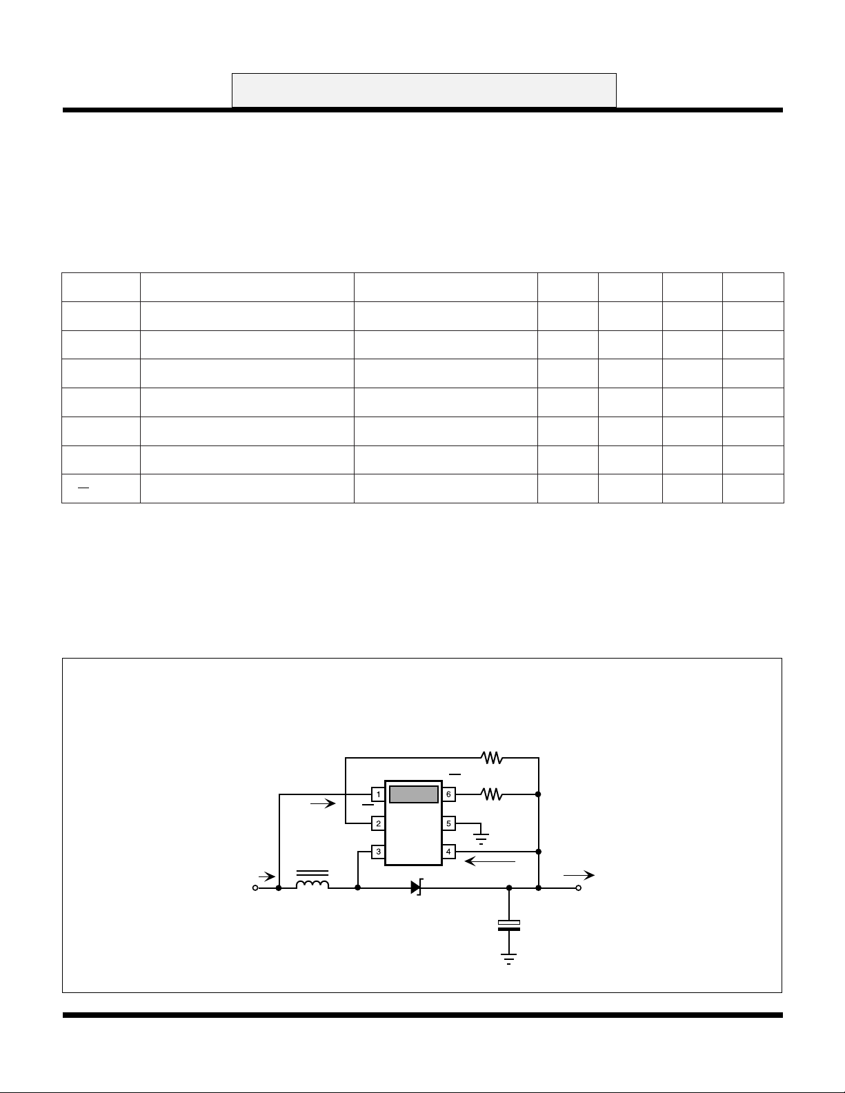
GENERAL CIRCUIT
V
LOI
300 kΩ
300 kΩ
OUTSW
I
I(V
)
OUT
OUT
V
OUT
C
V
IN
I(VIN)
I
B
V
IN
L
LBI GND
D
Page 2 January 1999 TOKO, Inc.
Page 3
ADVANCED INFORMATION
FINAL TEST CIRCUIT
TK652xx
300 kΩ
LOI
300 kΩ
GND
V
OUTSW
R
OF
15
++
C
U
10 µF
C
10 µF
I
OUT
V
OUT
D
C
N
10 µF
I
B
V
IN
L = 95 µF
Note: Inductor L: Toko A682AE-014 or equivalent
Diode D: LL101
Capacitors CN:CD:CU: Panasonic TE series,
ECS-TOJY106R
V
IN
LBI
C
S
220 pF
R
1 K
D
S
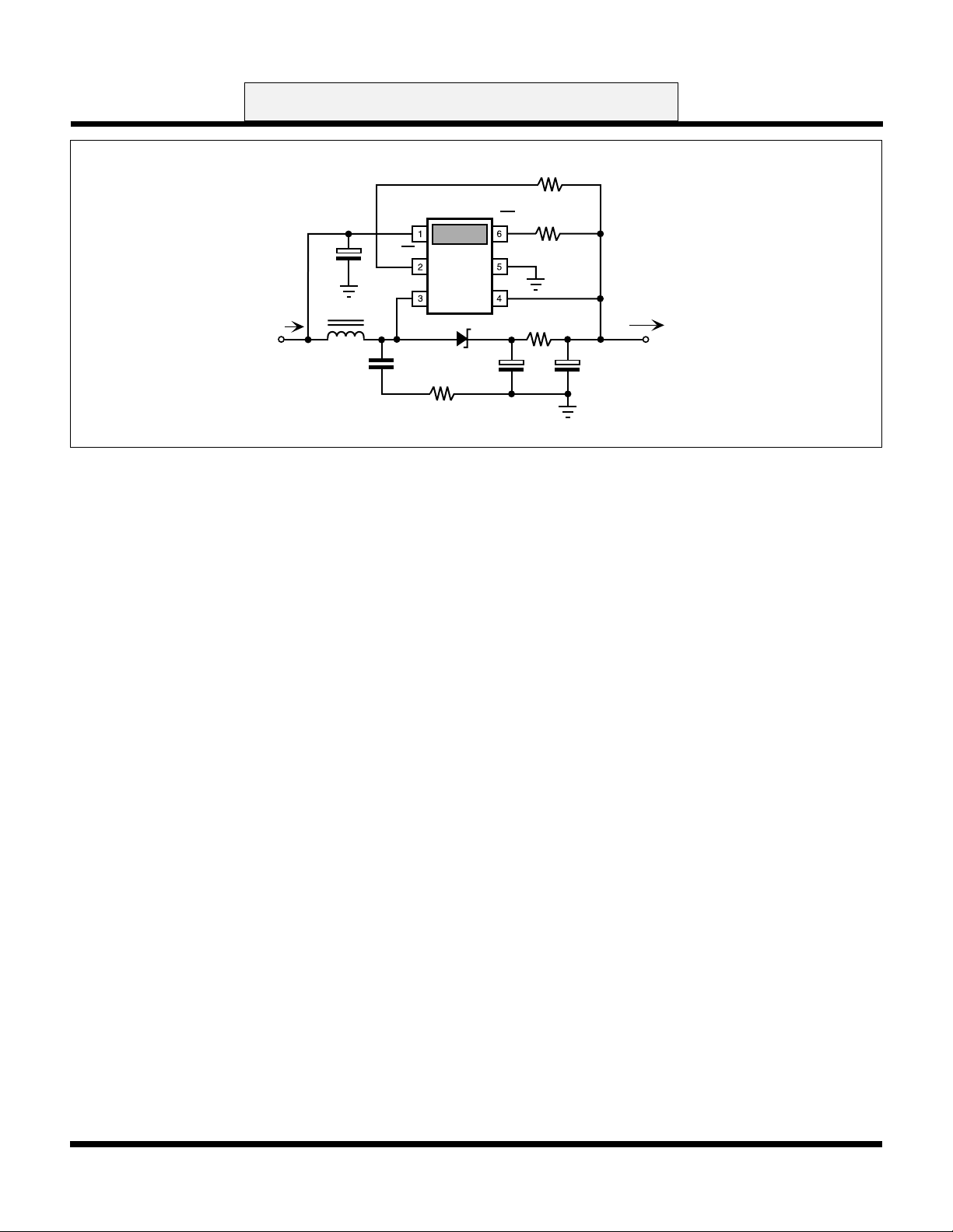
Above is the Final Test Circuit through which each of the production parts must pass. In this test circuit, the part is tested
against the specification limits in the data sheet (the min. and max. values in the Electrical Characteristics) at room
temperature, and is rejected if the tested values are outside the minimum (min.) and maximum (max.) values.
The Bench Test Circuits shown on the following pages are the circuits used most of the time to measure the typical (typ.)
values in the Electrical Characteristics section, and make the Typical Performance graphs.
Note: In measuring the oscillator frequency and the Max I
skipping” mode was achieved.
on the bench, the converter was loaded until “no pulse
OUT
January 1999 TOKO, Inc. Page 3
Page 4
TK652xx
ADVANCED INFORMATION
TK65218 ELECTRICAL CHARACTERISTICS
Over operating temperature range and supply voltage range, unless otherwise specified.
LOBMYSRETEMARAPSNOITIDNOCTSETNIMPYTXAMSTINU
I
)Q(B
V(INI)VotnitnerruCtnecseiuQ
V(I
)VotnitnerruCtnecseiuQ
TUO
∆f
/∆T
CSO
V
∆V
V
∆V
R
TUO
)GER(TUO
/∆T
)IOL(TUO
)IOL(TUO
)NO(WS
FFE)3,2setoN(ycneiciffEretrevnoC
V
VLU
V
NI
)3etoN(tnerruCyrettaBdaoLoN
T
A
V
niP
NI
niPVNI,V3.1=I
TUO
VfodlohserhTnoitalugeR
TUO
VfoytilibatSerutarepmeT
V
TUO
V
)IOL(TUO
noitisnarTIOLgniruDV
siseretsyHdlohserhTT
niPWSfoecnatsiser-nOV
egatloVtuokcoLegatlovrednUT
NI
T
A
rotallicsOfoytilibatSerutarepmeTV
NI
T
A
V
)GER(TUO
NI
NI
A
TUO
V
NI
A
V
NI
V
NI
,V3.1=I
TUO
C°52=
,V3.1=I
TUO
C°52=
TUO
,V3.1=
,Am0=
,Am4ot0=
0406Aµ
1102Aµ
Am0=2102Aµ
gnippikSesluPoN
1.0C°/%
C°52=647.1008.1548.1V
,V3.1=I
TUO
T,V3.1=
A
Am1=001C°/mpp
C°52=55.126.186.1V
C°52=52Vm
V=
,T
)GER(TUO
A
I,V3.1=
TUO
C°52=0.1mho
,Am6=
lioC37D,Hµ001=L
67%
)4etoN(,C°52=74.097.0V
T,V9.0=
A
T,V1.1=
A
,C°52=
lioCFD3,Hµ59=L
,C°52=
lioCFD3,Hµ59=L
50.7Am
60.31Am
ImumixaM
I
)XAM(TUO
TUO
)3,1setoN(
Inductor L: Toko A682AE-014 or equivalent
Diode D: LL103A or equivalent
Capacitors CN:CO:CB: Panasonic TE series,
ECS-TOJY106R
V
R
N
1 K
I
B
IN
I(VIN)
C
N
10 µF
L = 95 µH
C
B
10 µF
retrevnoCrof
V
NI
T,V3.1=
A
lioCFD3,Hµ59=L
V
NI
T,V9.0=
A
lioC37D,Hµ93=L
V
NI
T,V1.1=
A
lioC37D,Hµ93=L
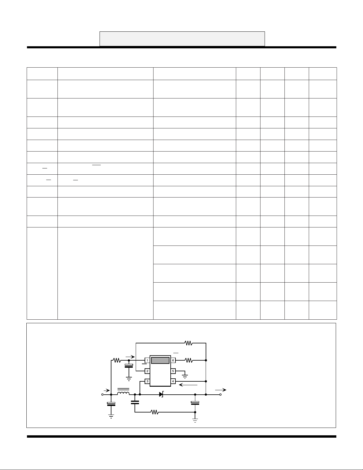
BENCH TEST CIRCUIT
300 kΩ
V
IN
LBI GND
C
S
220 pF
R
S
1 K
LOI
300 kΩ
V
OUTIND
I(V
)
OUT
D
C
10 µF
O
I
OUT
,C°52=
,C°52=
,C°52=
70.51Am
0.71Am
0.82Am
Note 1: Maximum load current depends on
inductor value and input voltages.
Note 2: Output ripple depends on filter
capacitor values, ESRs and the
inductor value.
Note 3: When using specified Toko inductor
and Schottky diode with VF = 0.45 V
@ 100 mA.
Note 4: Regulation not guaranteed.
V
OUT
Page 4 January 1999 TOKO, Inc.
Page 5
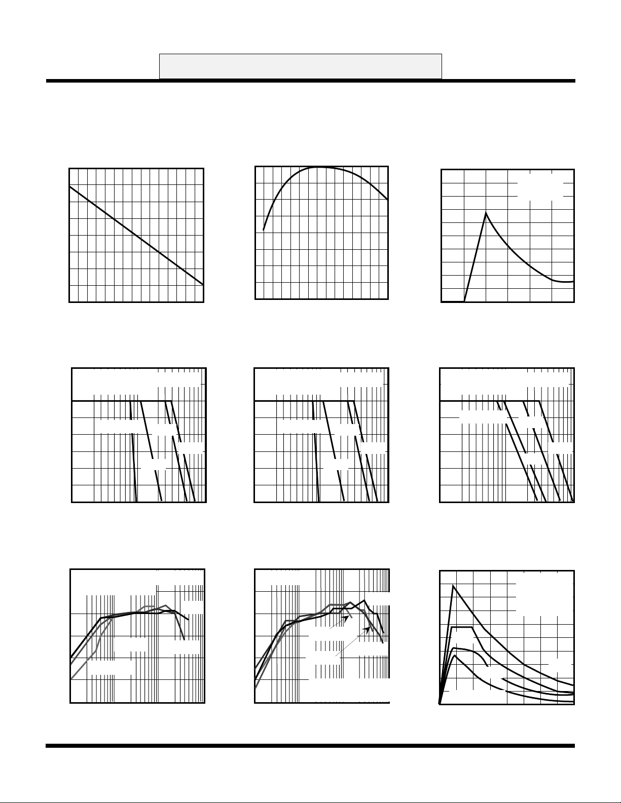
TK65218
V
(V)
V
(V)
V
(V)
ADVANCED INFORMATION
TYPICAL PERFORMANCE CHARACTERISTICS
TK652xx
OSCILLATOR FREQUENCY
TEMPERATURE
91
87
(kHz)
83
OSC
f
79
75
-50 0 50 100
TEMPERATURE (°C)
OUTPUT VOLTAGE
LOAD CURRENT
1.9
L = 95 µH
TOKO P/N: A682AE-014
(3DF SERIES)
TA = 25 °C
1.8
V
1.7
IN
= 0.9 V
1.3 V
OUT
1.6
1.1 V
VS.
VS.
1.6 V
OUTPUT REGULATION VOLTAGE
TEMPERATURE
1.800
1.795
(V)
1.790
OUT(REG)
V
1.785
1.780
-50 0 50 100
TEMPERATURE (°C)
OUTPUT VOLTAGE
LOAD CURRENT
1.9
L = 100 µH
TOKO P/N: 636CY-101M
(D73F SERIES)
TA = 25 °C
1.8
V
1.7
IN
= 0.9 V
1.3 V
OUT
1.6
1.1 V
VS.
1.6 V
VS.
BATTERY CURRENT
INPUT VOLTAGE
200
TA = 25 °C
160
NO LOAD
120
(µA)
B
I
80
40
0
0.1 0.5 1.0 1.5
VIN (V)
OUTPUT VOLTAGE
LOAD CURRENT
1.9
L = 39 µH
TOKO P/N: 636CY-390M
(D73 SERIES)
TA = 25 °C
1.8
V
= 0.9 V
IN
1.3 V
1.7
OUT
1.1 V
1.6
VS.
VS.
1.6 V
1.5
1 10 100
I
(mA)
OUT
EFFICIENCY VS. LOAD CURRENT
80
L = 95 µF
TOKO P/N: A682AE-014
(3DF SERIES) SMALL COIL
75
TA = 25 °C
70
65
EFF (%)
1.1 V
60
VIN = 0.9 V
55
50
0.1 1 10 100
I
(mA)
OUT
1.6 V
1.3 V
1.5
1 10 100
I
(mA)
OUT
EFFICIENCY
85
TA = 25 °C
VS.
LOAD CURRENT
80
75
70
VIN = 0.9 V
EFF (%)
65
60
55
1.1 V
L = 100 µF
TOKO P/N: A636CY-101M
(D73 SERIES) LARGER COIL
0.1 1 10 100
I
(mA)
OUT
1.6 V
1.3 V
1.5
1 10 100
I
(mA)
OUT
MAXIMUM OUTPUT CURRENT
INDUCTOR VALUE
100
NO PULSE
SKIPPING
MODE
TA = 25 °C
(mA)
80
60
1.3
40
OUT(MAX)
I
20
0
1.1 V
VIN = 0.9 V
0 40 80 120 160
INDUCTOR VALUE (µH)
VS.
1.6 V
January 1999 TOKO, Inc. Page 5
Page 6
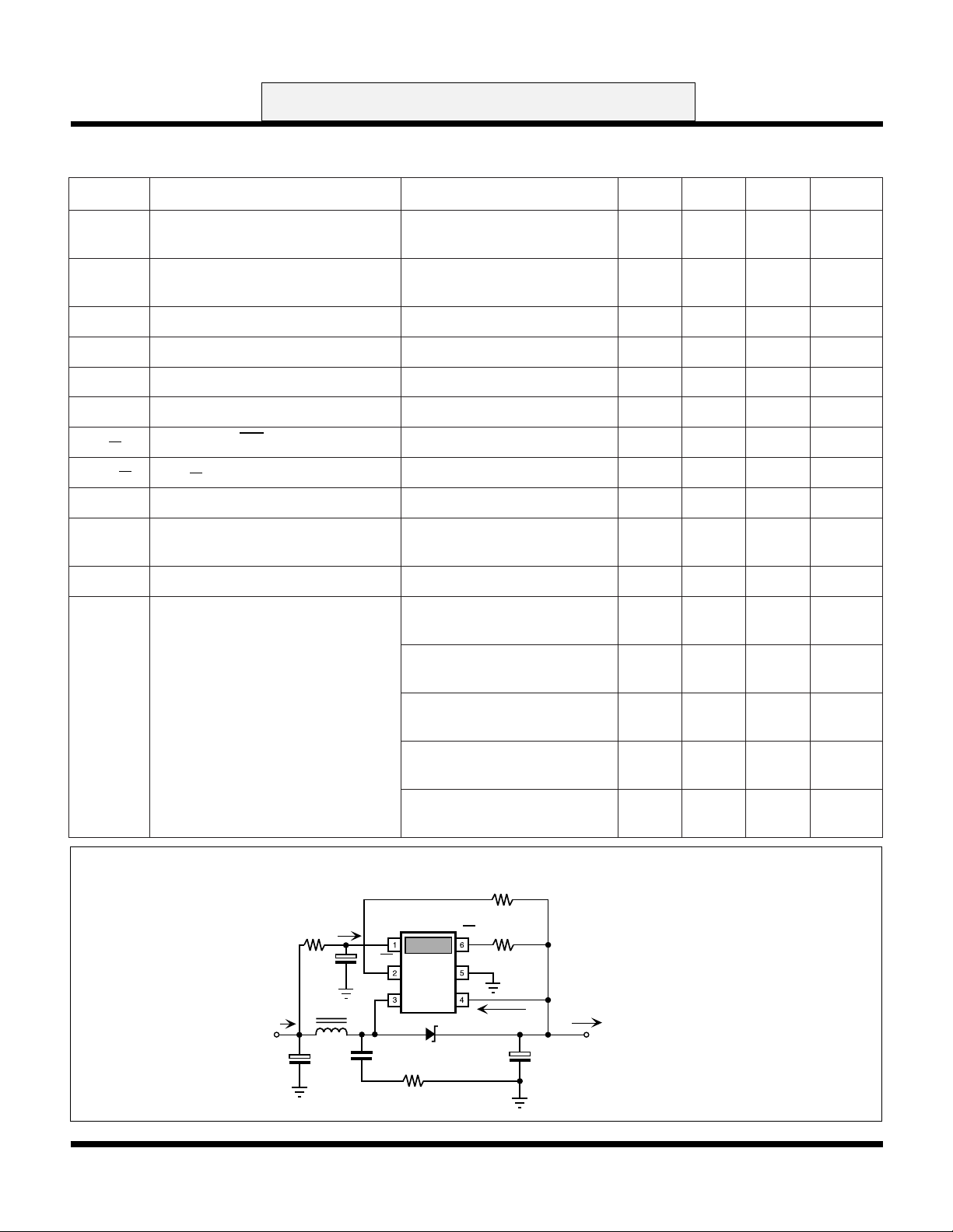
TK652xx
ADVANCED INFORMATION
TK65221 ELECTRICAL CHARACTERISTICS
Over operating temperature range and supply voltage range, unless otherwise specified.
LOBMYSRETEMARAPSNOITIDNOCTSETNIMPYTXAMSTINU
I
)Q(B
V(INI)VotnitnerruCtnecseiuQ
V(I
)VotnitnerruCtnecseiuQ
TUO
∆f
/∆T
CSO
V
∆V
V
∆V
R
TUO
)GER(TUO
/∆T
)IOL(TUO
)IOL(TUO
)NO(WS
FFE)3,2setoN(ycneiciffEretrevnoC
V
VLU
V
NI
)3etoN(tnerruCyrettaBdaoLoN
T
A
V
niP
NI
niPVNI,V3.1=I
TUO
VfodlohserhTnoitalugeR
TUO
VfoytilibatSerutarepmeT
V
TUO
V
)IOL(TUO
noitisnarTIOLgniruDV
siseretsyHdlohserhTT
niPWSfoecnatsiser-nOV
egatloVtuokcoLegatlovrednUT
NI
T
A
rotallicsOfoytilibatSerutarepmeTV
NI
T
A
V
)GER(TUO
NI
NI
A
TUO
V
NI
A
V
NI
V
NI
,V3.1=I
TUO
C°52=
,V3.1=I
TUO
C°52=
TUO
,V3.1=
,Am0=
,Am4ot0=
5456Aµ
5.2102Aµ
Am0=5.4132Aµ
gnippikSesluPoN
1.0C°/%
C°52=830.2001.2361.2V
,V3.1=I
TUO
T,V3.1=
A
Am1=001C°/mpp
C°52=38.198.159.1V
C°52=83Vm
V=
,T
)GER(TUO
A
,V3.1=I
TUO
C°52=0.1mho
,Am6=
lioC37D,Hµ001=L
87%
)4etoN(,C°52=84.097.0V
T,V9.0=
A
T,V1.1=
A
,C°52=
lioCFD3,Hµ59=L
,C°52=
lioCFD3,Hµ59=L
40.6Am
50.11Am
ImumixaM
I
)XAM(TUO
TUO
)3,1setoN(
Inductor L: Toko A682AE-014 or equivalent
Diode D: LL103A or equivalent
Capacitors CN:CO:CB: Panasonic TE series,
ECS-TOJY106R
I
B
V
IN
R
N
1 K
C
10 µF
L = 95 µH
C
10 µF
retrevnoCrof
V
NI
V
NI
V
NI
T,V3.1=
A
T,V9.0=
A
T,V1.1=
A
BENCH TEST CIRCUIT
300 kΩ
LOI
300 kΩ
V
OUTIND
I(V
OUT
B
N
I(VIN)
V
IN
LBI GND
C
220 pF
D
S
R
S
1 K
,C°52=
lioCFD3,Hµ59=L
,C°52=
lioC37D,Hµ93=L
,C°52=
lioC37D,Hµ93=L
60.31Am
0.51Am
0.42Am
Note 1: Maximum load current depends on
inductor value and input voltages.
Note 2: Output ripple depends on filter
capacitor values, ESRs and the
inductor value.
Note 3: When using specified Toko inductor
and Schottky diode with VF = 0.45 V
@ 100 mA.
Note 4: Regulation not guaranteed.
I
C
10 µF
OUT
V
OUT
O
)
Page 6 January 1999 TOKO, Inc.
Page 7
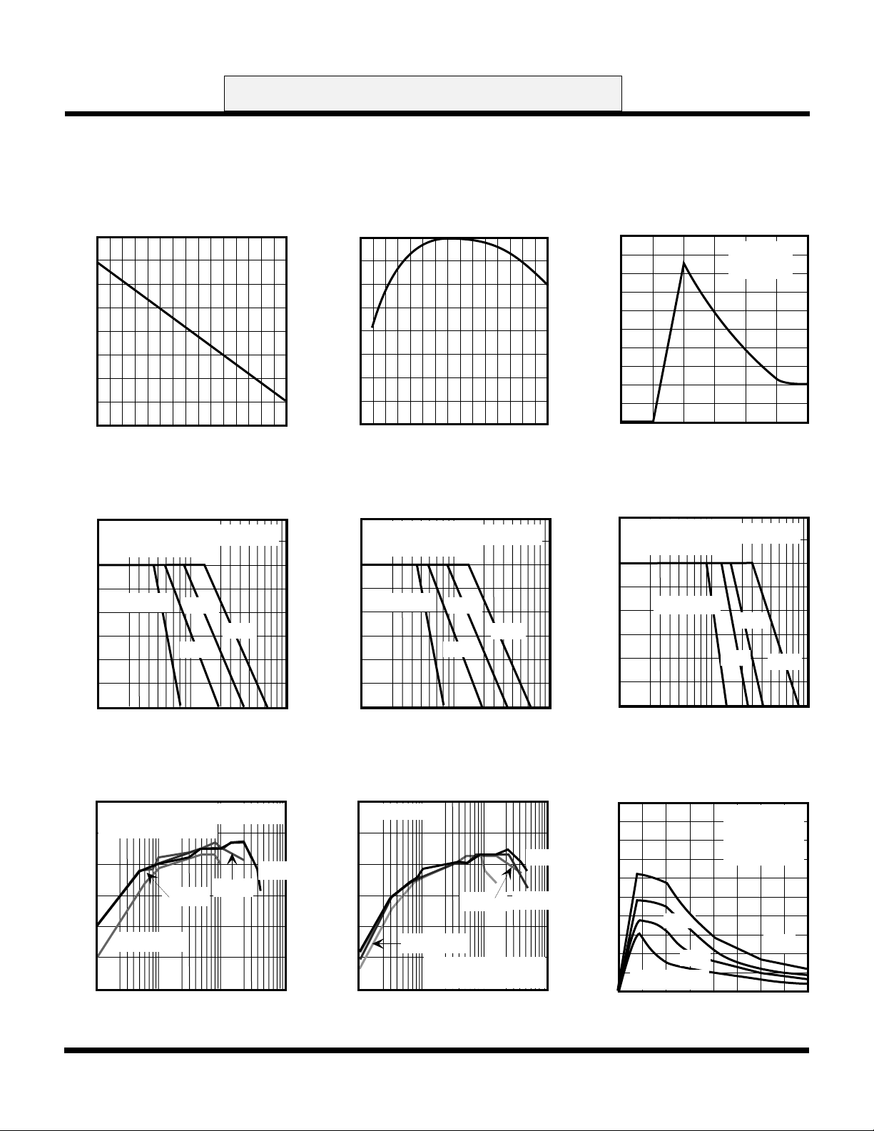
TK65221
V
(V)
V
(V)
V
(V)
ADVANCED INFORMATION
TYPICAL PERFORMANCE CHARACTERISTICS
TK652xx
OSCILLATOR FREQUENCY
TEMPERATURE
91
87
(kHz)
83
OSC
f
79
75
-50 0 50 100
TEMPERATURE (°C)
OUTPUT VOLTAGE
2.2
L = 95 µH
TOKO P/N: A682AE-014
(3DF SERIES)
LOAD CURRENT
TA = 25 °C
2.1
OUT
2.0
1.9
V
IN
= 0.9 V
1.3 V
1.6 V
1.1 V
VS.
VS.
OUTPUT REGULATION VOLTAGE
TEMPERATURE
2.100
2.095
(V)
2.090
OUT(REG)
V
2.085
2.080
-50 0 50 100
TEMPERATURE (°C)
OUTPUT VOLTAGE
LOAD CURRENT
2.2
L = 100 µH
TOKO P/N: 636CY-101M
(D73F SERIES)
TA = 25 °C
2.1
2.0
V
IN
= 0.9 V
1.3 V
OUT
1.9
1.1 V
VS.
1.6 V
VS.
BATTERY CURRENT
INPUT VOLTAGE
200
TA = 25 °C
160
NO LOAD
120
(µA)
B
I
80
40
0
0.1 0.5 1.0 1.5
VIN (V)
OUTPUT VOLTAGE
LOAD CURRENT
2.2
L = 39 µH
TOKO P/N: A636CY-390M
(D73 SERIES)
TA = 25 °C
2.1
2.0
OUT
1.9
V
IN
= 0.9 V
1.3 V
1.1 V
VS.
VS.
1.6 V
1.8
1 10 100
I
(mA)
OUT
EFFICIENCY VS. LOAD CURRENT
80
L = 95 µF
TOKO P/N: A682AE-014
(3DF SERIES) SMALL COIL
75
TA = 25 °C
70
65
1.1 V
1.3 V
EFF (%)
60
VIN = 0.9 V
55
50
0.1 1 10 100
I
(mA)
OUT
1.6 V
1.8
1 10 100
I
(mA)
OUT
EFFICIENCY VS. LOAD CURRENT
85
TA = 25 °C
80
75
70
EFF (%)
1.1 V
65
VIN = 0.9 V
60
55
L = 100 µF
TOKO P/N: A636CY-101M
(D73 SERIES) LARGER COIL
0.1 1 10 100
I
(mA)
OUT
1.6 V
1.3 V
1.8
1 10 100
I
(mA)
OUT
MAXIMUM OUTPUT CURRENT
INDUCTOR VALUE
100
NO PULSE
SKIPPING
80
(mA)
60
40
OUT(MAX)
I
20
0
1.3
1.1 V
VIN = 0.9 V
MODE
TA = 25 °C
0 40 80 120 160
INDUCTOR VALUE (µH)
1.6 V
January 1999 TOKO, Inc. Page 7
VS.
Page 8
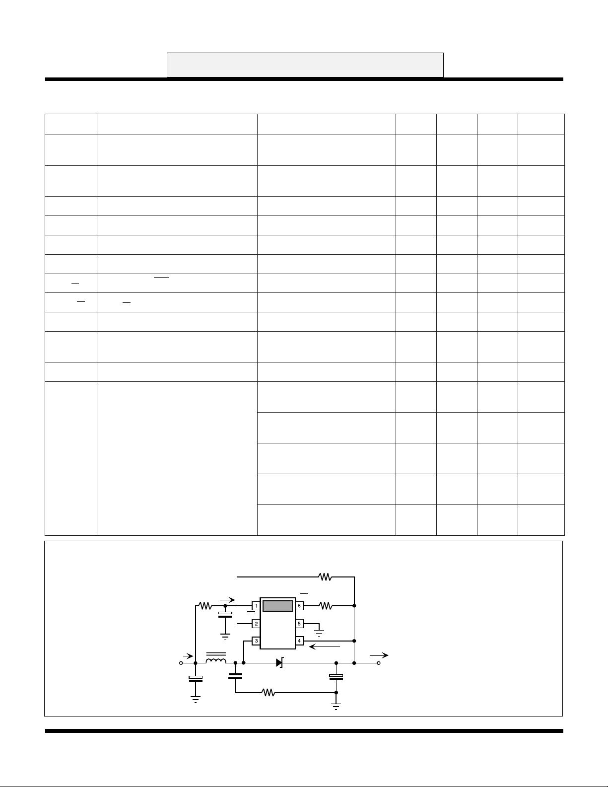
TK652xx
ADVANCED INFORMATION
TK65224 ELECTRICAL CHARACTERISTICS
Over operating temperature range and supply voltage range, unless otherwise specified.
LOBMYSRETEMARAPSNOITIDNOCTSETNIMPYTXAMSTINU
I
)Q(B
V(I
)VotnitnerruCtnecseiuQ
NI
V(I
)VotnitnerruCtnecseiuQ
TUO
∆f
/∆T
CSO
V
∆V
TUO
V
∆V
R
FFE)3,2setoN(ycneiciffEretrevnoC
V
VLU
/∆T
)IOL(TUO
)NO(WS
V
NI
)3etoN(tnerruCyrettaBdaoLoN
T
A
V
niP
NI
niPVNI,V3.1=I
TUO
)GER(TUO
VfodlohserhTnoitalugeR
TUO
VfoytilibatSerutarepmeT
V
TUO
V
)IOL(TUO
)IOL(TUO
noitisnarTIOLgniruDV
siseretsyHdlohserhTT
niPWSfoecnatsiser-nOV
egatloVtuokcoLegatlovrednUT
NI
T
A
rotallicsOfoytilibatSerutarepmeTV
NI
T
A
V
)GER(TUO
NI
NI
A
TUO
V
NI
A
V
NI
V
NI
,V3.1=I
TUO
C°52=
,V3.1=I
TUO
C°52=
TUO
,V3.1=
C°52=823.2004.2274.2V
,V3.1=I
TUO
T,V3.1=
A
C°52=05Vm
V=
,T
)GER(TUO
,V3.1=I
TUO
T,V9.0=
A
T,V1.1=
A
,Am0=
,Am4ot0=
5658Aµ
0253Aµ
Am0=2204Aµ
gnippikSesluPoN
1.0C°/%
Am1=001C°/mpp
C°52=70.261.252.2V
A
C°52=0.1mho
,Am6=
lioC37D,Hµ001=L
08%
)4etoN(,C°52=94.097.0V
,C°52=
lioCFD3,Hµ59=L
,C°52=
lioCFD3,Hµ59=L
57.30.5Am
5.40.9Am
ImumixaM
I
)XAM(TUO
TUO
)3,1setoN(
Inductor L: Toko A682AE-014 or equivalent
Diode D: LL103A or equivalent
Capacitors CN:CO:CB: Panasonic TE series,
ECS-TOJY106R
I
B
V
IN
retrevnoCrof
V
NI
V
NI
V
NI
BENCH TEST CIRCUIT
R
N
1 K
C
10 µF
L = 95 µH
C
10 µF
I(VIN)
N
B
V
IN
LBI GND
C
220 pF
D
S
R
S
1 K
LOI
V
OUTIND
T,V3.1=
T,V9.0=
T,V1.1=
300 kΩ
300 kΩ
I(V
A
A
A
,C°52=
lioCFD3,Hµ59=L
,C°52=
lioC37D,Hµ93=L
,C°52=
lioC37D,Hµ93=L
5.50.21Am
0.31Am
0.12Am
Note 1: Maximum load current depends on
inductor value and input voltages.
Note 2: Output ripple depends on filter
capacitor values, ESRs and the
inductor value.
Note 3: When using specified Toko inductor
and Schottky diode with VF = 0.45 V
@ 100 mA.
Note 4: Regulation not guaranteed.
I
C
10 µF
OUT
V
OUT
O
OUT
)
Page 8 January 1999 TOKO, Inc.
Page 9
TK65224
V
(V)
ADVANCED INFORMATION
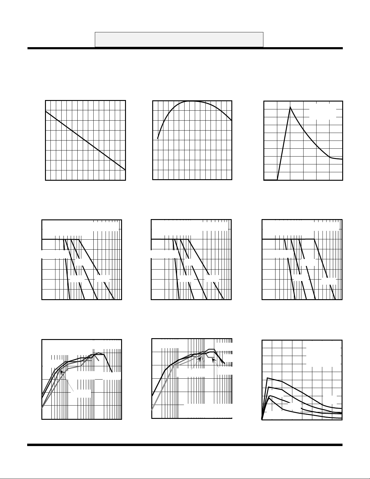
TYPICAL PERFORMANCE CHARACTERISTICS
TK652xx
OSCILLATOR FREQUENCY
TEMPERATURE
91
87
(kHz)
83
OSC
f
79
75
-50 0 50 100
TEMPERATURE (°C)
OUTPUT VOLTAGE VS.
2.5
L = 95 µH
TOKO P/N: A682AE-014
(3DF SERIES)
LOAD CURRENT
TA = 25 °C
2.4
V
(V)
OUT
V
2.3
2.2
IN
= 0.9 V
1.3 V
1.1 V
1.6 V
VS.
OUTPUT REGULATION VOLTAGE
TEMPERATURE
2.400
2.395
(V)
2.390
OUT(REG)
V
2.385
2.380
-50 0 50 100
TEMPERATURE (°C)
OUTPUT VOLTAGE VS.
LOAD CURRENT
2.5
L = 100 µH
TOKO P/N: 636CY-101M
(D73 SERIES)
TA = 25 °C
2.4
V
(V)
OUT
V
2.3
2.2
IN
= 0.9 V
1.3 V
1.1 V
1.6 V
VS.
BATTERY CURRENT
INPUT VOLTAGE
200
TA = 25 °C
160
NO LOAD
120
(µA)
B
I
80
40
0
0.1 0.5 1.0 1.5
VIN (V)
OUTPUT VOLTAGE
LOAD CURRENT
2.5
L = 39 µH
TOKO P/N: 636CY-390M
(D73 SERIES)
TA = 25 °C
2.4
V
2.3
OUT
2.2
IN
= 0.9 V
1.3 V
1.1 V
VS.
VS.
1.6 V
2.1
1 10 100
I
(mA)
OUT
EFFICIENCY VS. LOAD CURRENT
80
L = 95 µF
TOKO P/N: A682AE-014
(3DF SERIES) SMALL COIL
75
1.3 V
70
65
VIN = 0.9 V
TA = 25 °C
EFF (%)
60
1.1 V
55
50
0.1 1 10 100
I
(mA)
OUT
1.6 V
2.1
1 10 100
I
(mA)
OUT
EFFICIENCY VS. LOAD CURRENT
80
TA = 25 °C
80
75
VIN = 0.9 V
70
EFF (%)
65
60
55
L = 100 µF
TOKO P/N: A636CY-101M
(D73 SERIES) LARGER COIL
0.1 1 10 100
I
(mA)
OUT
1.3 V
1.6 V
1.1 V
2.1
1 10 100
I
(mA)
OUT
MAXIMUM OUTPUT CURRENT
INDUCTOR VALUE
100
NO PULSE
SKIPPING
MODE
TA = 25 °C
(mA)
80
60
40
20
0
1.3
1.1 V
VIN = 0.9 V
OUT(MAX)
I
0 40 80 120 160
INDUCTOR VALUE (µH)
VS.
1.6 V
January 1999 TOKO, Inc. Page 9
Page 10
TK652xx
ADVANCED INFORMATION
SINGLE-CELL APPLICA TION
The TK652xx is a boost converter control IC with the power
MOSFET switch built into the device. It operates from a
single battery cell and steps up the output voltage to a
regulated 1.8, 2.1 and 2.4 V. The device operates at a fixed
nominal clock frequency of 83 kHz.
In its simplest form, a boost power converter using the
TK652xx requires only three external components: an
inductor, a diode, and a capacitor.
The analysis is easier to follow when referencing the
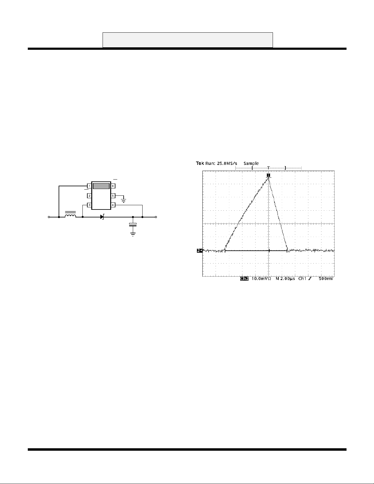
simple boost circuit below.
V
IN
LBI GND
LOI
V
OUTSW
V
+
OUT
FIGURE 1: SIMPLE BOOST CONVERTER
filtering component values (consult the “Ripple and Noise
Considerations” section) can be determined if needed or
desired.
The TK652xx runs with a fixed oscillator frequency and it
regulates by applying or skipping pulses to the internal
power switch. This regulation method is called Pulse Burst
Modulation (PBM).
ANALYSIS OF SWITCHING CYCLE
I
PEAK
di/dt = VIN / L
t (on)
di/dt = - (V
t (off)
+ Vf - VIN)/ L
OUT
t (deadtime)
THEORY OF OPERATION
The converter operates with one terminal of an inductor
connected to the DC input and the other terminal connected
to the switch pin of the IC. When the switch is turned on, the
inductor current ramps up. When the switch is turned off (or
“lets go” of the inductor), the voltage flies up as the inductor
seeks out a path for its current. A diode, also connected to
the switching node, provides a path of conduction for the
inductor current to the boost converter’s output capacitor.
The TK652xx monitors the voltage of the output capacitor
and has a 1.8, 2.1 and 2.4 V threshold at which the
converter switching becomes deactivated. So the output
capacitor charges up to 1.8, 2.1 and 2.4 V and regulates
there, provided that no more current is drawn from the
output than the inductor can provide. The primary task,
then, in designing a boost converter with the TK652xx
is to determine the inductor value (and its peak current
rating to prevent inductor core saturation problems)
which will provide the amount of current needed to
guarantee that the output voltage will be able to
maintain regulation up to a specified maximum load
current. Secondary necessary tasks also include choosing
the diode and the output capacitor. Then the snubber and
Above is the input or inductor current waveform over a
switching cycle.
From an oscillator standpoint, the switching cycle consists
of only an on-time and an off-time. But from an inductor
current standpoint, the switching cycle breaks down into
three important sections: on-time, off-time, and deadtime.
The on-time of the switch and the inductor current are
synonymous. During the on-time, the inductor current
increases. During the off-time, the inductor current
decreases as it flows into the output. When the inductor
current reaches zero, that marks the end of the inductor
current off-time. For the rest of the cycle, the inductor
current remains at zero. Since no energy is being either
stored or delivered, that remaining time is called “deadtime.”
This mode of the inductor current decaying to zero every
cycle is called “discontinuous mode.” In summary, energy
is stored in the inductor during on-time, delivered to the
output during off-time, and remains at zero during deadtime.
The output current of the boost converter comes from the
Page 10 January 1999 TOKO, Inc.
Page 11

ADVANCED INFORMATION
SINGLE-CELL APPLICATION (CONT.)
TK652xx
second half of the input current triangle waveform (averaged
over the period or multiplied by the frequency) given by the
equation:
I
= [IPK x t(off)] x f / 2
OUT
and:
IPK = (VIN / L) x t(on) = V
IN
D / f L
and:
t(off) = IPK / [(V
= (V
= V
D / f L) / [(V
IN
D / f (V
IN
+ VF - VIN) / L]
OUT
OUT
+ VF - VIN)
OUT
+ VF - VIN) / L]
therefore:
I
= (VIN)2 (D)2 / 2 f L (V
OUT
+ VF - VIN)
OUT
which derives Equation 1 of the next section.
INDUCTOR SELECTION
It is under the condition of lowest input voltage that the
boost converter output current capability is the lowest for
a given inductance value. Three other significant
parameters with worst-case values for calculating the
inductor value are: highest switching frequency, lowest
duty ratio (of the switch on-time to the total switching
period), and highest diode forward voltage. Other
parameters which can affect the required inductor value,
but for simplicity will not be considered in this first analysis
are: the series resistance of the DC input source (i.e., the
battery), the series resistance of the internal switch, the
series resistance of the inductor itself, ESR of the output
capacitor, input and output filter losses, and snubber
power loss.
The converter reaches maximum output current capability
when the switch runs at the oscillator frequency, without
pulses being skipped. The output current of the boost
converter is then given by the equation:
2
+ VF - VIN)
(1)
I
OUT
=
2
f
L (V
(VIN)2 (D)
OUT
where “VIN” is the input voltage, “D” is the on-time duty ratio
of the switch, “f ” is the switching (oscillator) frequency, “L”
is the inductor value, “V
” is the output voltage, and “VF”
OUT
is the diode forward voltage. It is important to note that
Equation 1 makes the assumption stated in Equation 2:
VIN ≤ (V
+ VF)(1 - D)
OUT
(2)
The implication from Equation ) is that the inductor will
operate in discontinuous mode.
Now, plugging in worst case conditions, the inductor value
can be determined by simply transforming the above
equation in terms of “L”:
L
(MIN)
=
2
f
V
(MAX) IOUT(MAX)
IN(MIN)
[V
OUT(MIN)
2
D
(MIN)
+ V
2
F(MAX)
- V
IN(MIN)
]
(3)
where “V
” is best approximated by the diode forward
F(MAX)
voltage at about two-thirds of the peak diode current value.
The peak diode current is the same as the peak input
current, the peak switch current, and the peak inductor
current. The formula is:
VIN D
IPK =
f
L
(4)
Some reiteration is implied because “L” is a function of “VF”
which is a function of “IPK” which, in turn, is a function of “L”.
The best way into this loop is to first approximate “VF”,
determine “L”, determine “IPK”, and then determine a new
“VF”. Then, if necessary, reiterate.
When selecting the actual inductor, it is necessary to make
sure the peak current rating of the inductor (i.e., the current
which causes the core to saturate) is greater than the
maximum peak current the inductor will encounter. To
determine the maximum peak current, use Equation 4
again, using the maximum values for “VIN” and “D”, and
minimum values for “f ” and “L”.
It may also be necessary when selecting the inductor to
check the rms current rating of the inductor. Whereas peak
January 1999 TOKO, Inc. Page 11
Page 12

TK652xx
ADVANCED INFORMATION
SINGLE-CELL APPLICATION (CONT.)
current rating is determined by core saturation, rms current
rating is determined by wire size and power dissipation in
the wire resistance. The inductor rms current is given by:
IPK f L
I
= I
L(RMS)
(5)
where “IPK” is the same maximized value that was just used
to check against inductor peak current rating, and the term
in the numerator within the radical that is added to the
[on-time] duty ratio, “D”, is the off-time duty ratio.
PK
D +
V
OUT
+ VF - V
3
IN
Toko America, Inc. can offer a miniature matched
magnetic solution
sizes to accommodate varying power level requirements.
The following series of Toko inductors work especially well
with the TK652xx : 10RF, 12RF, 3DF, D73, and D75. The
5CA series can be used for isolated-output applications,
although such design objectives are not considered here.
OTHER CONVERTER COMPONENTS
In choosing a diode, parameters worthy of consideration
are: forward voltage, reverse leakage, and capacitance.
The biggest efficiency loss in the converter is due to the
diode forward voltage. A Schottky diode is typically chosen
to minimize this loss. Possible choices for Schottky diodes
are: LL103A from ITT MELF case; 1N5017 from Motorola
(through hole case); MBR0530 from Motorola (surface
mount) or 15QS02L from Nihon EC (surface mount).
Reverse leakage current is generally higher in Schottkys
than in pin-junction diodes. If the converter spends a good
deal of the battery lifetime operating at very light load (i.e.,
the system under power is frequently in a standby mode),
then the reverse leakage current could become a substantial
fraction of the entire average load current, thus degrading
battery life. So don’t dramatically oversize the Schottky
diode if this is the case.
Diode capacitance isn’t likely to make much of an
undesirable contribution to switching loss at this relatively
low switching frequency. It can, however, increase the
snubber (look in the “Ripple and Noise Considerations”
section) dissipation requirement.
The output capacitor, the capacitor connected from the
diode cathode to ground, has the function of averaging the
in a wide range of inductor values and
current pulses delivered from the inductor while holding a
relatively smooth voltage for the converter load. Typically,
the ripple voltage cannot be made smooth enough by this
capacitor alone, so an output filter is used. In any case, to
minimize the dissipation required by the output filter, the
output capacitor should still be chosen with consideration
to smoothing the voltage ripple. This implies that its
Equivalent Series Resistance (ESR) should be low. This
usually means choosing a larger size than the smallest
available for a given capacitance. To determine the peak
ripple voltage on the output capacitor for a single switching
cycle, multiply the ESR by the peak current which was
calculated in Equation 4. ESR can be a strong function of
temperature, being worse case when cold. The capacitance
should be capable of integrating a current pulse with little
ripple. Typically, if a capacitor is chosen with reasonably
low ESR, and if the capacitor is the right type of capacitor
for the application (typically aluminum electrolytic or
tantalum), then the capacitance will be sufficient.
ESR and printed circuit board layout have strong influence
on RF interference levels. Special care must be taken to
optimize PCB layout and component placement.
THE BENEFITS OF INPUT FILTERING
In practice, it may be that the peak current (calculated in
Equation 4) flowing out of the battery and into the converter
will cause a substantial input ripple voltage dropped across
the resistance inside the battery. This becomes a more
likely case for cold temperature (when battery series
resistance is higher), higher load rating converters (whose
inductors must draw higher peak currents), and when the
battery is undersized for the peak current application.
While the simple analysis used a parameter “VIN” to
represent the converter input voltage in the equations, one
may not know what “VIN” value to use if it is delivered by a
battery that allows high ripple to occur. For example,
assume that the converter draws a peak current of 100 mA
for a 1 V input, and assume that the input is powered by a
partially discharged AAA battery which might have a series
resistance of 2 Ohms at 0 °C. (Environmentally clean, so
called “green” batteries tend to have higher source
resistance than their “unclean” predecessors). If such
partially discharged battery voltage is 1 V without load, the
converter battery voltage will sag to about 0.8 V during the
on-time. This can cause two problems: 1) with the effective
input voltage to the converter reduced in this way, the
converter output current capability will decrease, 2) if the
Page 12 January 1999 TOKO, Inc.
Page 13

ADVANCED INFORMATION
SINGLE-CELL APPLICATION (CONT.)
TK652xx
same battery is powering the TK652xx at the VIN pin (i.e.,
the normal case), then the IC may become inoperable due
to insufficient VIN. This is why the application test circuit
features an RC filter into the VIN pin. The current draw is
very small, so the voltage drop across this filter resistor is
negligible. The filter serves to average out the input ripple
caused by the battery resistance. Note that this filter is
optional, and the net effect of its use is the extension of
battery life by allowing the battery to be discharged more
deeply.
A more power-efficient method comes at the price of a
large capacitor. This can be placed in parallel with the
battery to help channel the converter current pulses away
from the battery. The capacitor must have low ESR
compared to the battery resistance in order to accomplish
this effectively.
Still another solution is to filter the DC input with an LC
filter. However, it is more likely that the filter will be either
too large or too lossy. It is of questionable benefit to smooth
the input if the DC loss through the filter is large.
Assuming that input ripple voltage at the battery terminal
and converter input is large, and that we filter the VIN pin of
the IC as in the test circuit, then the parameter “VIN” in the
previous equations is not usable, and we will need to use
parameters to represent both the source voltage
source resistance.
SWITCH ON-RESISTANCE, INDUCTOR WINDING
RESISTANCE, AND CAPACITANCE ESR
The on-resistance of the TK652xx’s internal switch is
about 1 Ohm maximum. Using the previously stated
example of 100 mA peak current, the voltage drop across
the switch would reach 100 mV during the on-time. This
subtracts from the voltage which is impressed across the
inductor to store energy during the on-time. As a result,
less energy is delivered to the output during the off-time.
If the winding resistance of the inductor increases to 1 Ohm
or greater, the voltage drop across the winding resistance
also subtracts from the voltage used to store energy in the
core. Thus, efficiency degradation occurs.
As the inductor delivers energy into the output capacitor
during the off-time, its current decays at a rate proportional
to the voltage drop across it. The idealized equations
assume that the voltage at the switching node is clamped
and
the
at a diode drop above the output voltage. However, the
ESR of the output capacitor can increase the voltage drop
across the inductor by the additional voltage dropped
across the ESR when the peak current flows in it. For
example, the voltage across a capacitor with an ESR of 2
Ohms (not unusual at cold temperature) would jump by
200 mV when 100 mA peak current began to flow in it. This
extra voltage drop would cause the inductor current to
ramp down more quickly, thus, depleting the available
output current. Possible choices for low ESR capacitors
are: Panasonic TE series (surface mount); AVX TPS
series (surface mount); Matsuo 267 series (surface mount);
Sanyo OS-CON series.
LBI AND LOI FEATURES
In a properly designed system that has its maximum load
current under the limit of the maximum output current of the
converter, the Low Battery Indicator (LBI) signal is the first
indicator that the battery is getting low. The latched Low
Output indicator (LOI) signal is the second and final
indicator that the battery should be replaced.
The LBI output provides a warning signal to a system
controller that the battery is near the end of its life and will
need replacing soon. The LBI threshold voltage is between
1.05 and 1.15 V. There is no hysteresis in its on-off trigger
levels.
The LOI output can provide a reset signal to a microprocessor or other external system controller. When the
output voltage falls below the LOI threshold (during startup of the converter or under a current overload fault
condition), the LOI signal is asserted low, indicating that
the system controller )e.g., microprocessor) should be in a
reset mode. This method of reset control can be used to
prevent improper system operation which might occur at
low supply voltage levels. The LOI threshold voltage is
between 87% and 93% of the regulated output voltage
value. The LOI threshold also has about 40 mV hysteresis
between its on-off trigger levels.
When the output voltage dips below the LOI threshold and
the LBI signal is asserted low, the LOI signal will be
latched low by the LBI signal. That is, the LOI signal will
remain asserted low until the LBI signal goes high,
even if the output voltage regains its regulated value.
Although the converter can start-up and work with the
battery voltage even as low as 0.9 V, the battery should
be replaced when the LOI is latched low.
January 1999 TOKO, Inc. Page 13
Page 14
TK652xx
ADVANCED INFORMATION
SINGLE-CELL APPLICATION (CONT.)
RIPPLE AND NOISE CONSIDERATIONS
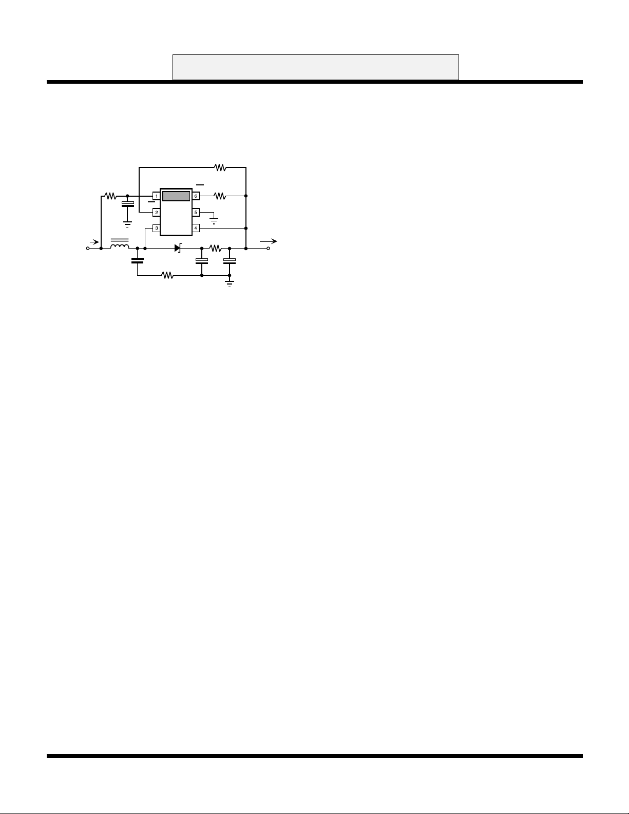
The filtered test circuit of the TK652xx is shown below in
Figure 2.
300 kΩ
V
R
N
1 K
C
N
10 µF
I
B
V
IN
L = 95 µF
IN
LBI GND
C
S
220 pF
R
1 K
FIGURE 2: FILTERED TEST CIRCUIT
Compared to the simple boost circuit, this Filtered Test
Circuit adds the following circuitry: the RC filter into the V
pin, the RC snubber, the RC filter at the converter output,
and the pull-up resistor to the LOI pin.
The RC filter at the VIN pin is used only to prevent the ripple
voltage at the battery terminals from prematurely causing
undervoltage lockout of the IC. This is only needed when
the inductor value is relatively small and the battery
resistance is relatively high and the VIN range must extend
as low as possible.
The snubber (optional) is composed of a series RC network
from the switch pin to ground (or to the output or input if
preferred). Its function is to dampen the resonant LC circuit
which rings during the inductor current deadtime. When
the current flowing in the inductor through the output diode
decays to zero, the parasitic capacitance at the switch pin
from the switch, the diode, and the inductor winding has
energy which rings back into the inductor, flowing back into
the battery. If there is no snubbing, it is feasible that the
switch pin voltage could ring below ground. Although the
IC is well protected against latch-up, this ringing may be
undesirable due to radiated noise. To be effective, the
snubber capacitor should be large (e.g., 5 - 20 times) in
comparison to the parasitic capacitance. If it is unnecessarily
large, it dissipates extra energy every time the converter
switches. The resistor of the snubber should be chosen
such that it drops a substantial voltage as the ringing
parasitic capacitance attempts to pull the snubber capacitor
along for the ride. If the resistor is too small (e.g., zero), the
snubber capacitance just adds to the ringing energy. If the
resistor is too large (e.g., infinite), it effectively disengages
the snubber capacitor from fighting the ringing.
LOI
300 kΩ
V
OUTSW
I
C
10 µF
OUT
V
OUT
D
R
OF
15
++
D
S
C
10 µF
U
The RC filter at the converter output attenuates the
conducted noise; the converter may not require this.
Finally, the pull-up resistors at the LOI pin are needed only
if this output signals is used. Most of this circuitry which
appears in the test circuit has been added to minimize
ripple and noise effects. But when this is not critical, the
circuit can be minimized.
When any DC-DC converter is used to convert power in RF
circuits (e.g., pagers) the spectral noise generated by the
converter, whether conducted or radiated, is of concern.
The oscillator of the TK652xx has been trimmed and
stabilized to 83 +/- 4 kHz with the intention of greatly
minimizing interference at the common IF frequency of
455 kHz.
In comparison with conventional IC solutions, where the
oscillator frequency is not controlled tightly, the TK652xx
IN
can achieve as much as 20 - 30 dB improvements in RF
interference reduction by means of its accurately controlled
oscillator frequency. This IF frequency is halfway between
the fifth and sixth harmonics of the oscillator. The fifth
harmonic of the maximum oscillator frequency and the
sixth harmonic of the minimum oscillator frequency still
leave a 39 kHz band centered around 455 kHz within which
a fundamental harmonic of the oscillator will not fall. Since
the TK652xx operates by pulse burst modulation (PBM),
the switching pattern can be a subharmonic of the oscillator
frequency. The simplest example, and the one to be
avoided the most, is that of the converter causing every
other oscillator pulse to be skipped. This means that the
switching pattern would have a fundamental frequency of
one-half the oscillator frequency, or 41.5 kHz. This is the
eleventh harmonic, which lands at 456.5 kHz, right in the
IF band. Fortunately, the energy is rather weak at the
eleventh harmonic. Even more fortunate is the ease with
which that regulation mode is avoided.
The internal regulator comparator has a finite hysteresis.
When an additional output filter is used (e.g., the RC filter
of the test circuit, or an LC filter), the ripple at the regulation
node is minimized. This limits the rate at which the oscillator
can be gated. In practice, this means that rather than
exhibiting a switching pattern of skipping every other
oscillator pulse, it would be more likely to exhibit a switching
pattern of three or four pulses followed by the same
number of pulses skipped. Although this also tends to
increase the output ripple, it is low frequency and has low
magnitude (e.g., 10 kHz and 10 mV) which tends to be of
little consequence.
Page 14 January 1999 TOKO, Inc.
Page 15

ADVANCED INFORMATION
SINGLE-CELL APPLICATION (CONT.)
HIGHER-ORDER DESIGN EQUATION
TK652xx
2
]
OUT(TGT)
F
L
OF
S
BB
2
+ (V
+ VF)2 + (V
OUT
OUT
ƒCS [V
-
)
Targeted output current capability
Diode forward voltage
Inductor winding resistance
Output filter resistance
Snubber capacitance
2(V
OUT
+ VF)
+ VF - VBB)2 ]
(6)
D
(
D
2ƒ L
D
2ƒ L
capability
)
V
BB2
I
=
OUT
V
+ ROFI
OUT
The equation above was developed as a closed form approximation. In order to allow for a closed form, the design variable
that required the least approximation was “I
The approximations made in the equation development have the primary consequence that error is introduced as
resistive losses become relatively large. As it is normally a practical design goal to ensure that resistive losses will be
relatively small, this seems acceptable. The variables used are:
V
OUT(TGT)
I
Output current
OUT
Output voltage V
OUT
V
Battery voltage, unloaded D Oscillating duty ratio of main switch
BB
f
Oscillator frequency L Inductance value
R
Source resistance (battery + filter) R
S
R
Switch on-state resistance R
SW
R
ESR of upstream output capacitor C
U
+ (VBBRU) + VF - V
D
1- (RS + RL + RSW)
[
2ƒ L
D
1 - (RS+ RL)
(
BB
OUT
2ƒ L
,” as opposed to “L.”
I
Deriving a design solution with this equation is necessarily an iterative process. Use worst-case tolerances as described
for inductor selection, using different values for “L” to approximately achieve an “I
fine tune the parasitic values as needed and, if necessary, readjust “L” again and reiterate the process.
January 1999 TOKO, Inc. Page 15
” equal to the targeted value. Then,
OUT
Page 16
TK652xx
ADVANCED INFORMATION
STEP-DOWN CONVERTER APPLICATION
HOW TO MAKE A STEP-DOWN CONVERTER USING THE TK652xx AND AN IRF7524D1 “FETKY” PART
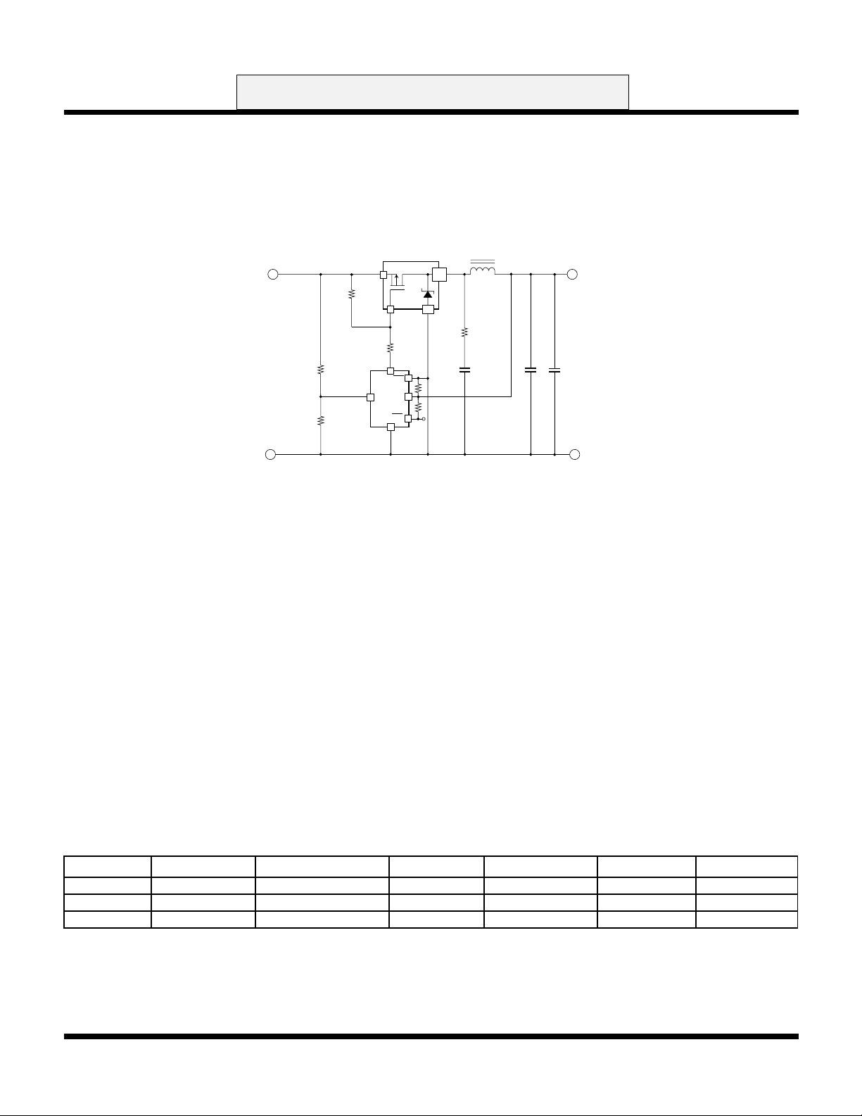
The TK652xx can be used as a controller in a step-down converter with the following two additional changes. See Fig 3.
V
BATT
R
10 k
R
3.9 k
1
2
R
1 k
U1
TK65221
V
U2
IRF7524D1
3
3
3
V
1
OUT
IN
LOI
5
GND
5,6,
7,8
1,24
R
4
150
SW
2
R
300 k
4
R
300 k
6
L1
V
120 µH
R
7
1 k
C
1
220 pFLBI
5
6
OUT
+
+
C2
47 µFC347 µF
Note: L = 120 µH
Toko P/N: 646CY-121M
D75C Coil
FIGURE 3: STEP-DOWN CONVERTER USING THE TK65221 SCHEMATIC
1) Change the main switch orientation for use in a step-down converter. An external P-channel power MOSFET is
used as the main switch in a step-down converter configuration. The gate of FET is turned on through a resistor divider
being pulled down to GND by the internal output transistor of the TK652xx. This application requires both a logic level
P-channel MOSFET and a Schottky diode. An IRF7524D1 “FETKY” part contains both in a small micro 8 package.
2) Change the voltage seen at the V
divider between the converter V
than the V
pin, the TK652xx will not regulate the output, but will continue to pulse its output transistor.
OUT
IN
pin of the TK652xx to below the regulation voltage at the V
IN
and the chip VIN pin drops the voltage seen at the VIN pin. If the VIN pin is a higher voltage
pin. A resistor
OUT
WHERE TO USE THIS STEP-DOWN CONVERTER
The TK65221 is a Pulse Burst Modulation (PBM) controller with a fixed duty cycle of approximately 50%. Therefore, only
if V
can and does regulate in DCM (discontinuous current mode) for lighter output current loads with V
voltage of V
is more than twice the voltage of V
BATT
. But DCM produces more peak current and more ripple current than CCM. Below is a table giving some
OUT
can the converter run in CCM (continuous current mode). The converter
OUT
less than twice the
IN
examples of where this type of step-down converter might be used.
Type Battery # of Cells V
Range V
BATT
OUT
Typ. Max I
Oper Mode Inductor
OUT
Li-ion 2 (Note 1) 5.4 to 8.4 V 2.1 V 500 mA CCM 120 µH
NiMH 4 (Note 2) 4.4 to 5.2 V 2.1 V 500 mA CCM 120 µH
NiMH 6 (Note 2) 6.6 to 7.8 V 2.1 V 500 mA CCM 120 µH
Note 1: Li-ion cell voltage range 2.7 V to 4.2 V
Note 2: NiMH cell voltage range 1.1 V to 1.3 V
Page 16 January 1999 TOKO, Inc.
Page 17
ADVANCED INFORMATION
TK652xx
STEP-DOWN CONVERTER APPLICATION (CONT.)
THE AMOUNT OF BOARD SPACE NEEDED TO IMPLEMENT THIS STEP-DOWN CONVERTER
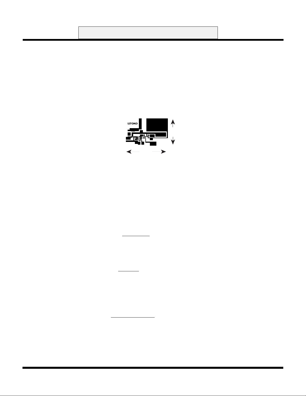
An evaluation board for this converter has been made using a TOKO D73 or D75 series inductor, using only 0.96 sq.
inches of board space. The artwork for the surface-mount circuit board is shown below in Figure 4.
Actual Size
VOUT
G
G
VIN
LOI
LBI
1.2 "
FIGURE 4: TK652xx STEP-DOWN CONVERTER EVALUATION BOARD ARTWORK
.8 "
SELECTING INPUT RESISTOR DIVIDER VALUES
Since the TK652xx draws so little quiescent current into VIN, relatively large resistance values can be used in the
input resistor divider. The following shows the relationship equation between V
and VIN pin of the TK652xx, and
BATT
an example method of finding the resistor values to be used in the resistor divider.
V
IN
(R1 + R2)
BATT
=
2
- R1 x (IQ of VIN)
V
X R
therefore:
R1 + R
2
V
BATT
=
R
x [ V
2
and typical (IQ of VIN) = 15 µA and typical LBI trigger value of VIN = 1.1 V and letting R1 = 10 k solving for R
=
V
BATT
- 1.25 V
R
2
10 k x 1.25 V
then for the case of 4 NiMH cells picks a LBI trigger at V
+ R1 x (IQ of VIN)]
IN
= 4.4 V, then R
BATT
= 3.97 k
2
:
2
(1)
January 1999 TOKO, Inc. Page 17
Page 18
TK652xx
ADVANCED INFORMATION
STEP-DOWN CONVERTER APPLICATION (CONT.)
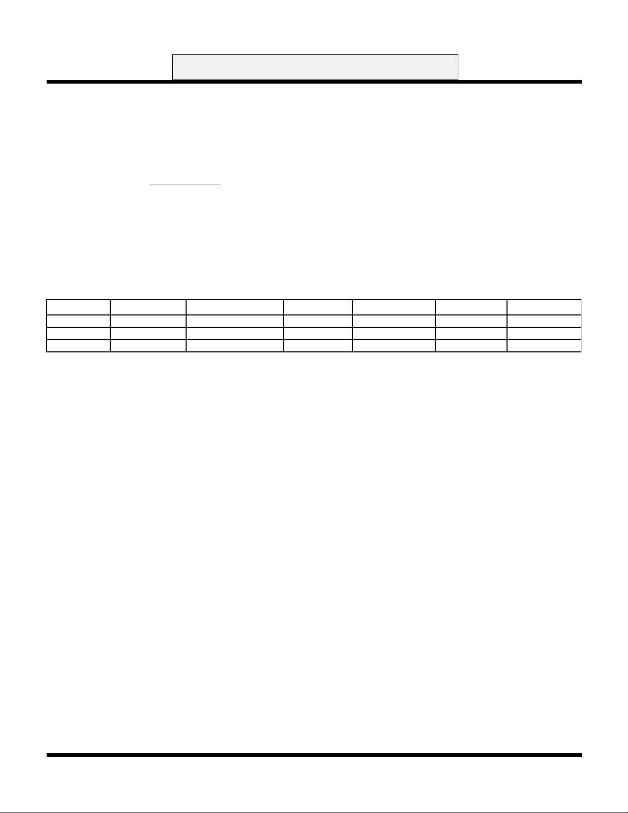
2) Now, after selecting the R1 and R2 values, check that the V
max V
is:
yes: 1.33 V < 2.1 V
Below are the resistor values for the three battery cases listed in “Where to use the TK652xx Step-Down Converter”
section.
Type Battery # of Cells V
Li-ion 2 5.4 to 8.4 V 2.1 V 10 K 3.01 K 1.79 V < 2.1
NiMH 4 4.4 to 5.2 V 2.1 V 10 K 3.97 K 1.33 V < 2.1
NiMH 6 6.6 to 7.8 V 2.1 V 10 K 2.34 K 1.33 V < 2.1
= 5.2 V and the TK65221 VIN > V
BATT
2.1V >
5.2 V x 3.97 k
10 k + 3.97 k
BATT
= 2.1 V, using the first equation.
REG
- 10 k x 15 µA
Range V
REG
is below V
IN
R1 VALUE ~R2 VALUE VIN CHECK
for the maximum V
REG
. For NiMH cells
BATT
Page 18 January 1999 TOKO, Inc.
Page 19
ADVANCED INFORMATION
TK652xx
PULSED LOAD APPLICATION
Often in the world of power conversion, the current draw of the load circuit is not constant, but rather pulsed. It is common
in power supply design to size the power path large enough, and make the feedback loop fast enough to support these
pulsed maximum currents. For applications where the pulse width is long or unpredictable, this approach may be
warranted. However, in applications where the pulse width and maximum frequency of occurrence is predictable, such
as digital cell phones or two-way pagers, it may be easier and wiser to increase the energy storage in the output filter
of the power supply and keep the power path small. This leads to the need for a very large value output capacitor.
Panasonic makes a series AL gold cap “super cap” which is a low voltage, large value capacitor in the one farad range.
Before designing a low power DC-DC converter with a “super cap” in its output filter, it is necessary to know the loading
profile (the waveform of the current going into the load from the output of the converter) of the application in which it is
to be used. The converter can then be designed so that the “super cap” can be recharged in the time before the next big
discharge current pulse comes along.
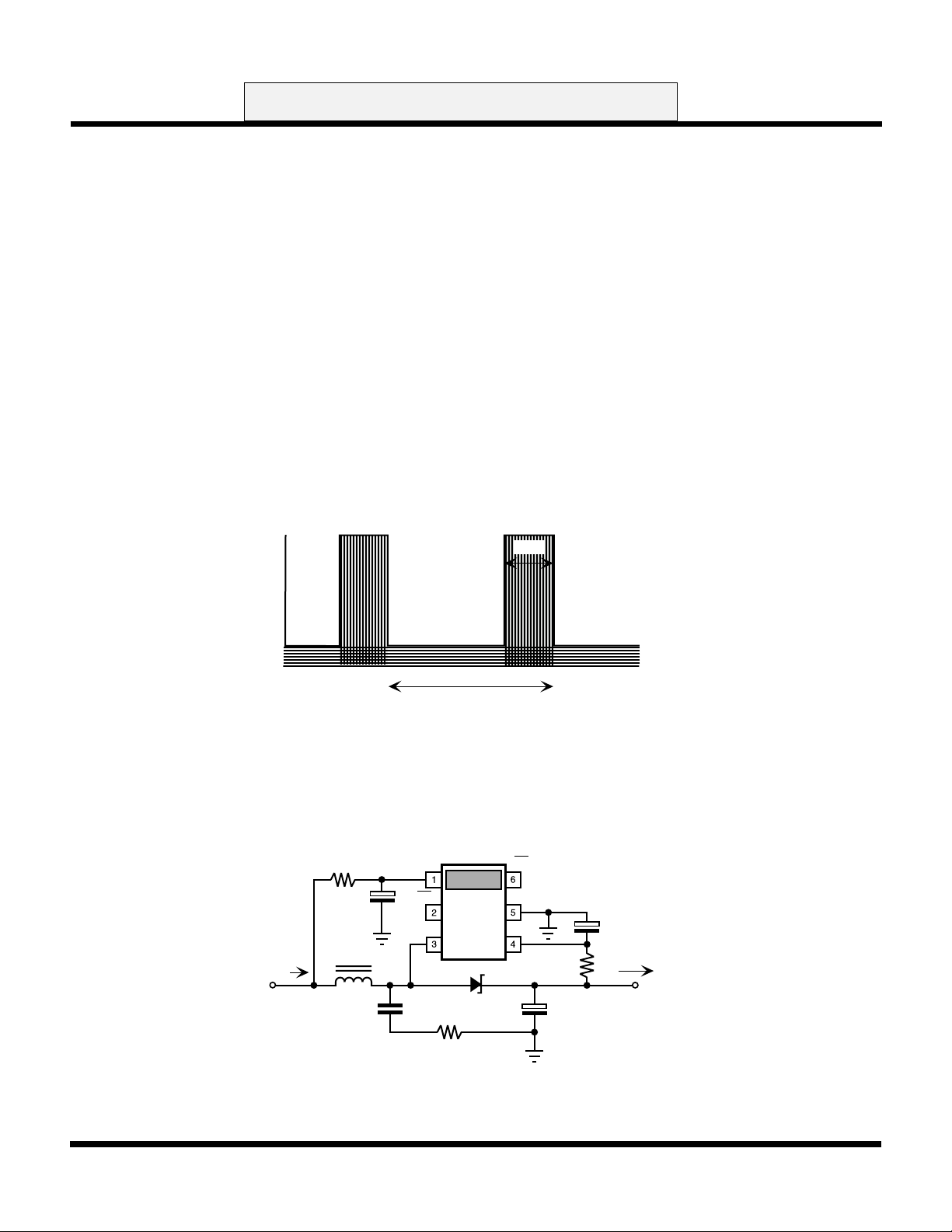
Figure 5 is an example “super cap” charge/discharge diagram showing that the charge into the cap needs to equal the
charge leaving the cap during discharge. This diagram comes from the loading and unloading profile information. In
reality, some extra charge needs to go into the cap to make up for the losses caused by ESR of the cap.
1A
60 ms
Note: Equal charge into and out of “supercap”
2 s (30 mA) = 60 ms (1A)
I
OUT
30 mA
time
2 s
FIGURE 5: “SUPER CAP” CHARGE/DISCHARGE DIAGRAM
Figure 6 is a schematic for this “super cap” example application.
R
N
1 k
C
N
10 µF
I
B
V
IN
L = 39 µF
V
IN
LBI GND
R
1 k
D
S
C
S
220 pF
V
LOI
OUTIND
+
"SUPERCAP"
GOLD CAP
1 F
Drawing not to scale
C
D
10 µF
+
I
OUT
V
OUT
FIGURE 6: PULSED LOAD “SUPER CAP” APPLICATION SCHEMATIC
January 1999 TOKO, Inc. Page 19
Page 20
TK652xx
ADVANCED INFORMATION
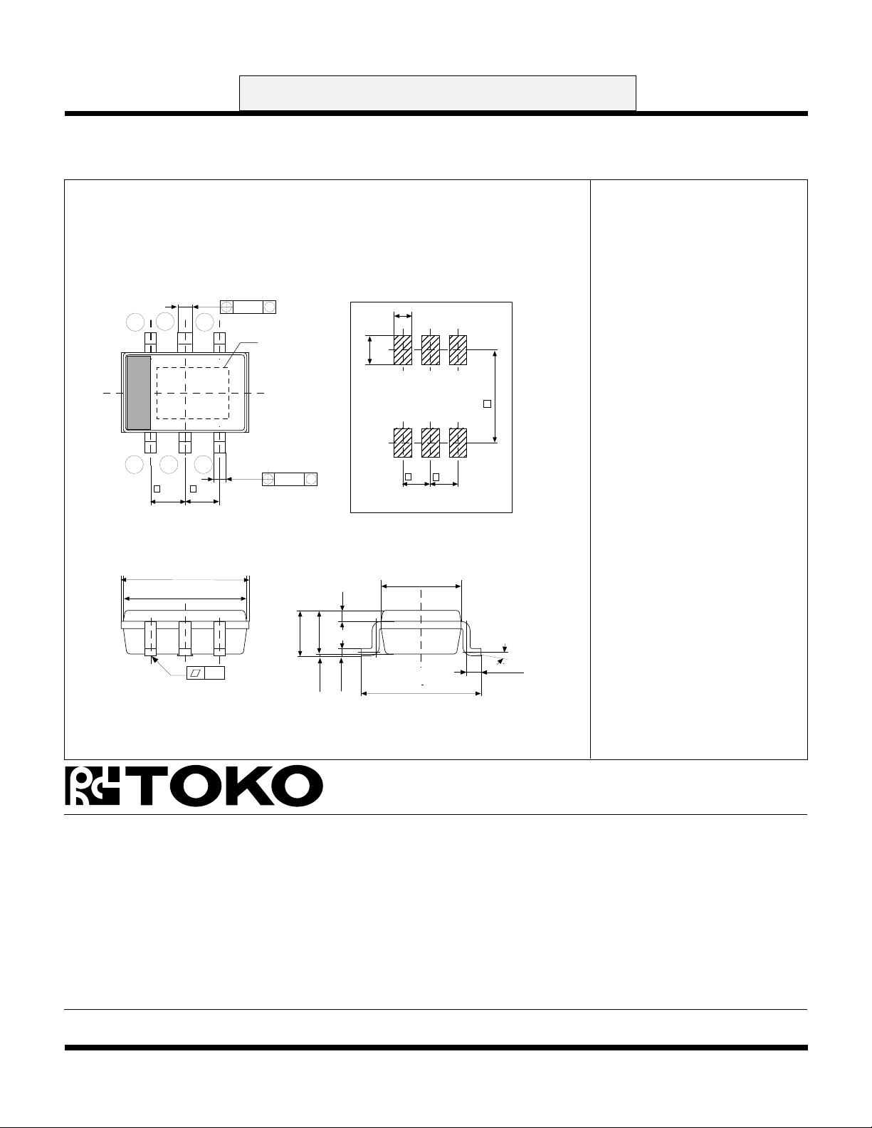
PACKAGE OUTLINE
SOT-23L-6
123
e e
0.95 0.95
Marking Information
Marking
TK65218 18M
TK65221 21M
+0.15
- 0.05
0.4
0.1
M
456
marking
+0.15
- 0.05
0.32
+0.3
- 0.1
3.5
3.4
5 PL
0.1
M
0.3
0.6
1.0
Recommended Mount Pad
ee
0.95 0.95
2.2
3.0
e1
TK65224 24M
0.1
Dimensions are shown in millimeters
Tolerance: x.x = ± 0.2 mm (unless otherwise specified)
1.4 max
1.2
0 ~ 0.1
+0.15
- 0.05
0.15
+ 0.3
3.3
max
15
0.4
Toko America, Inc. Headquarters
1250 Feehanville Drive, Mount Prospect, Illinois 60056
Tel: (847) 297-0070 Fax: (847) 699-7864
TOKO AMERICA REGIONAL OFFICES
Midwest Regional Office
Toko America, Inc.
1250 Feehanville Drive
Mount Prospect, IL 60056
Tel: (847) 297-0070
Fax: (847) 699-7864
Western Regional Office
Toko America, Inc.
2480 North First Street , Suite 260
San Jose, CA 95131
Tel: (408) 432-8281
Fax: (408) 943-9790
Eastern Regional Office
Toko America, Inc.
107 Mill Plain Road
Danbury, CT 06811
Tel: (203) 748-6871
Fax: (203) 797-1223
Semiconductor Technical Support
Toko Design Center
4755 Forge Road
Colorado Springs, CO 80907
Tel: (719) 528-2200
Fax: (719) 528-2375
Visit our Internet site at http://www.tokoam.com
The information furnished by TOKO, Inc. is believed to be accurate and reliable. However, TOKO reserves the right to make changes or improvements in the design, specification or manufacture of its
products without further notice. TOKO does not assume any liability arising from the application or use of any product or circuit described herein, nor for any infringements of patents or other rights of
third parties which may result from the use of its products. No license is granted by implication or otherwise under any patent or patent rights of TOKO, Inc.
Page 20 January 1999 TOKO, Inc.
All Rights Reserved
IC-xxx-TK652xx
0798O0.0K
Printed in the USA© 1999 Toko, Inc.
 Loading...