

Page 1
TK15327
Audio Analog Switch
FEATURES
■ Wide Operating Voltage Range (2 to 14 V)
■ Low Distortion (typ. 0.004%)
■ Wide Dynamic Range (typ. 6 V
P-P
)
■ Low Output Impedance (typ. 20 Ω)
■ Low Switching Noise (typ. 3 mV)
■ Output Parallel Connection Possible
DESCRIPTION
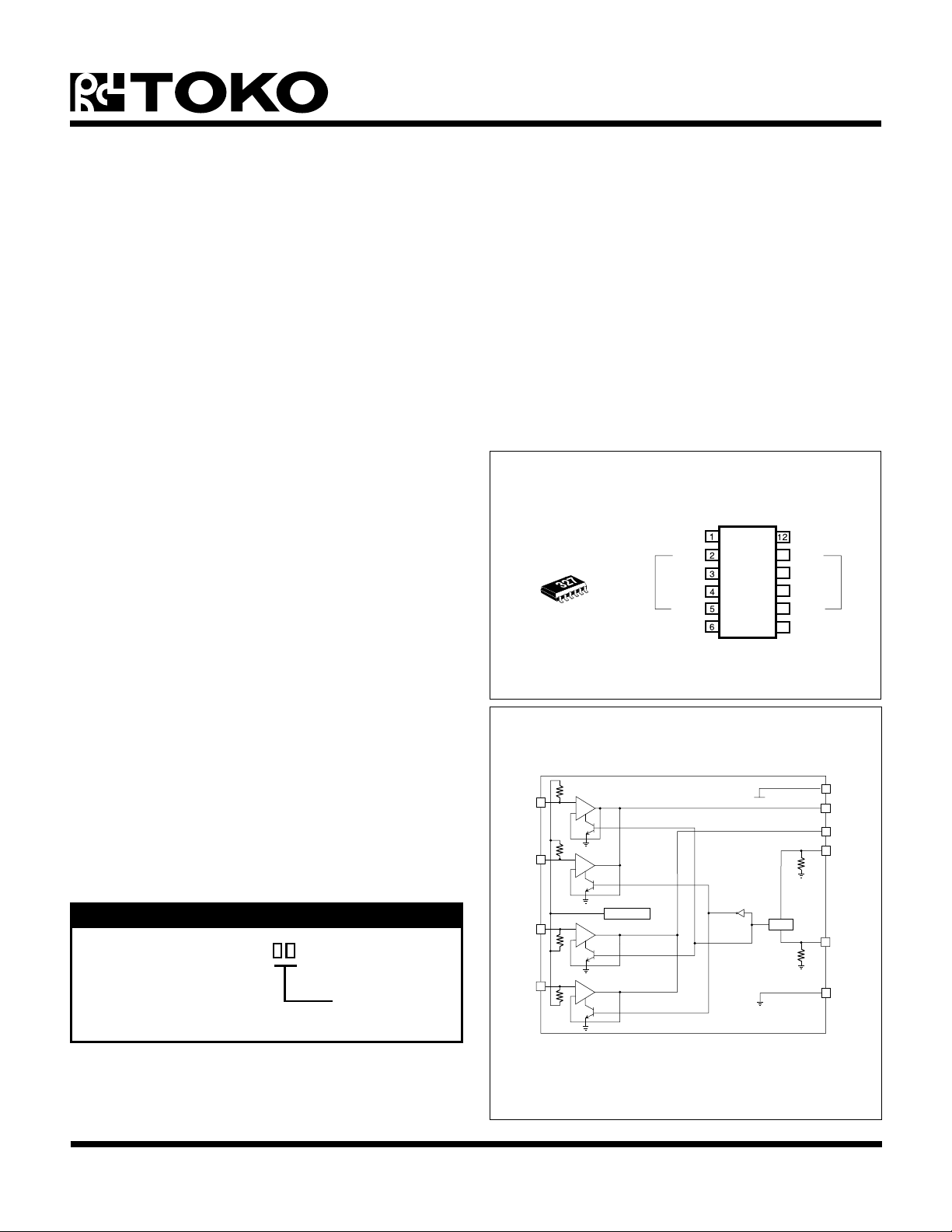
The TK15327M is an Analog Switch IC that was developed
for audio frequency. The function is to select one output
from two inputs and has a floating position too. The
channel can be changed by two control levels and the
device includes two circuits. The TK15327M has a
mono-power supply and the input bias is a built-in type
(VCC / 2 V). Because the distortion is very low, the TK15327M
fits various signals switching. It is best suited for Hi-Fi
devices. Operating voltage is wide, the circuit plan is
simple. The TK15327M is available in a small plastic
surface mount package (SSOP-12).
APPLICATIONS
■ Audio Systems
■ Radio Cassettes
1ch-in 2ch-in
TK15327
V
CC
Bch
OUT
Ach
1KEY
NC
GND
Bch
11
OUT
10
9
Ach
2 KEY
8
NC
7
BLOCK DIAGRAM
V
CC
1 ch out
2 ch out
1KEY
2KEY
GND
ORDERING INFORMATION
TK15327M
Tape/Reel Code
TAPE/REEL CODE
TL: Tape Left
1ch-in
2ch-in
Ach
Bch
Ach
Bch
+
-
+
-
Reg. (VCC / 2)
+
-
+
-
Logic
June 1999 TOKO, Inc. Page 1
Page 2
TK15327
ABSOLUTE MAXIMUM RATINGS
Supply Voltage ......................................................... 15 V
Power Dissipation (Note 4) ................................ 350 mW
Storage Temperature Range ................... -55 to +150 °C
ANALOG SWITCH SECTION
Signal Input Voltage ........................ -0.3 V to VCC + 0.3 V
Signal Output Current ............................................. 3 mA
Operating Temperature Range ...................-20 to +75 °C
CONTROL SECTION
Input Voltage ................................... -0.3 V to VCC + 0.3 V
Operating Voltage Range................................. 2 to 14 V
Maximum Input Frequency..................................100 kHz
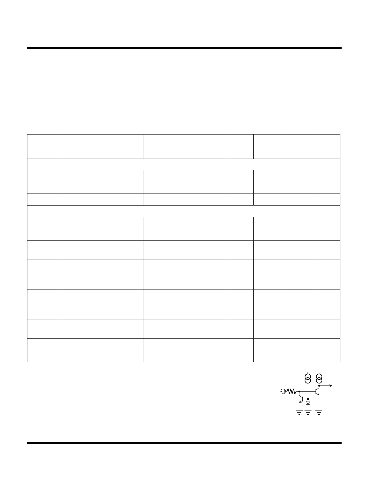
TK15327M ELECTRICAL CHARACTERISTICS
Test conditions: V
LOBMYSRETEMARAPSNOITIDNOCTSETNIMPYTXAMSTINU
I
CC
V
LI
V
HI
Z
NI
DHTnoitrotsiDcinomraHlatoTV
N
L
OSInoitalosI
= 8.0 V, T
CC
= 25 °C, unless otherwise specified.
A
tnerruCylppuS 2.45.6Am
NOITCESLORTNOCYEK
leveLwoLegatloVtupnI1etoN3.0-8.0+V
leveLhgiHegatloVtupnI8.1V
ecnadepmItupnI 05kΩ
NOITCESHCTIWSGOLANA
NI
esioNlaudiseR2etoN01smrVµ
V
NI
3etoN
3.0+V
CC
zHk1=f,smrV1=400.0800.0%
,zHk01=F,smrV1=
57-Bd
PESnoitarapeS
V
NI
3etoN
,zHk01=f,smrV1=
NYDleveLlangiStupnImumixaM%1.0=DHT,zHk1=f0.2smrV
AVGniaGegatloVzHk02~=f0Bd
V
tnec
∆V
tnec
R
NI
Z
TUO
Note 1: The KEY input equivalent circuit is shown to the right.
1 channel and 2 channel is the separate action by 1Key pin and
2 key pin. When the control pin is open, it is outputted high level (about 1.4 V). Then the A channel input
signal is outputted. The change is carried out at low level.
Note 2: The specification means a value as measurement-input terminal connects to ground through a capacitor.
Note 3: ISO is a cross talk between A channel and B channel, SEP is a cross talk between 1 channel and 2
channel. The specification means a value as measurement-input termianl connects to ground through 10
kΩ resistor and capacitor.
Note 4: Power dissipation is 350 mW when mounted as recommended. Derate at 3.0 mW/°C for operation above
25°C.
egatloV
ecnereffiD
lanimreTtuptuO-tupnI
egatloVlanimreTtuptuO
ecnatsiseRsaiBtupnI 56Aµ
ecnadepmItuptuOecnadepmICD02
V
CC
tuptuo2/8.30.42.4V
lennahcemasneewteB331Vm
Input Key
08-Bd
Ω
Logic
Page 2 June 1999 TOKO, Inc.
Page 3
SW9
SW8
TEST CIRCUITS AND METHODS
V
CC
SW6
SW3
10 µF
+
SW7
10 µF
SW4
+
TK15327
33 µF
+
SW2
1 kHz
1 Vrms
or
2 Vrms
~
10 kHz
1 Vrms
~
10 kΩ
SW5
V
V
_
~
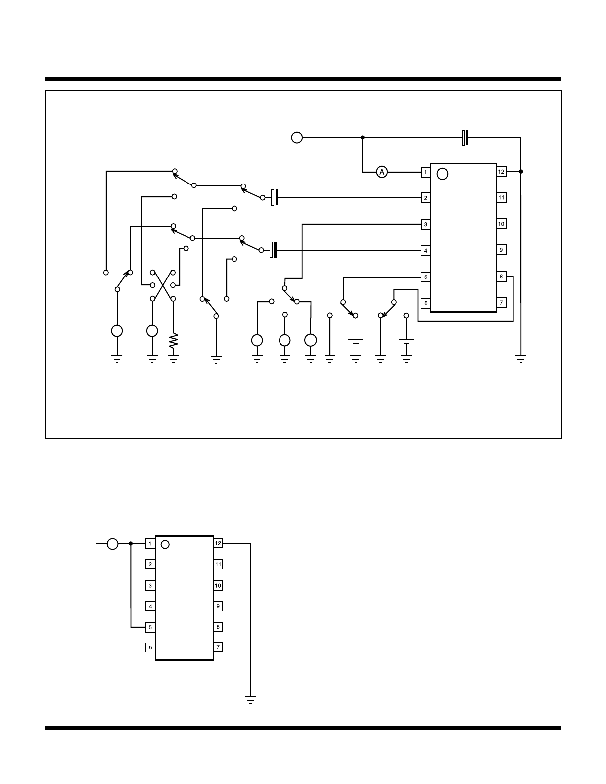
1: The above condition represents 1ch.
2: The above conditions distortion rate of 1-Ach and dynamic range measurement.
3: SW5 is for residual noise measurement.
4: SW8 is for cross talk (ISO or SEP) measurement.
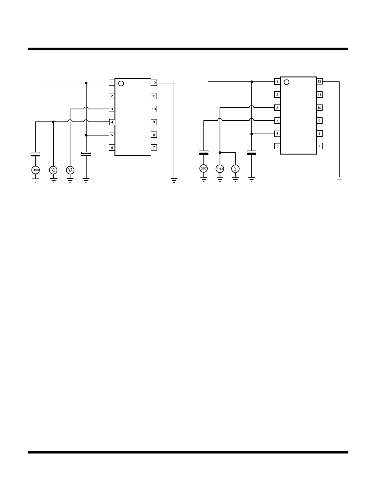
SUPPLY CURRENT (FIGURE 1)
This current is a consumption current with a nonloading
condition.
1) Connect Pin 5 to VCC, Pin 8 is low level or open.
1) Measure the inflow current to Pin 1 from VCC. This
current is the supply current.
AV
CC
SW1
LH
THD
LH
CONTROL LOW/HIGH LEVEL (FIGURE 2)
This level is to measure the threshold level.
1) Input, the VCC to Pin 1. (This condition is the same with
other measurements, omitted from the next for simplicity)
2) Input to Pin 4 with sine wave (f = 1 kHz, VIN = 1 Vrms).
3) Connect an oscilloscope to Pin 3.
4) Elevate the control voltage from 0 V gradually (Pin 8 is
low level or open), until the sine wave appears at the
oscilloscope. This voltage is the threshold level when
the wave appears.
Figure 1
June 1999 TOKO, Inc. Page 3
Page 4
TK15327
V
CC
++
TEST CIRCUITS AND METHODS (CONT.)
V
CC
++
~
Cont.
Figure 2
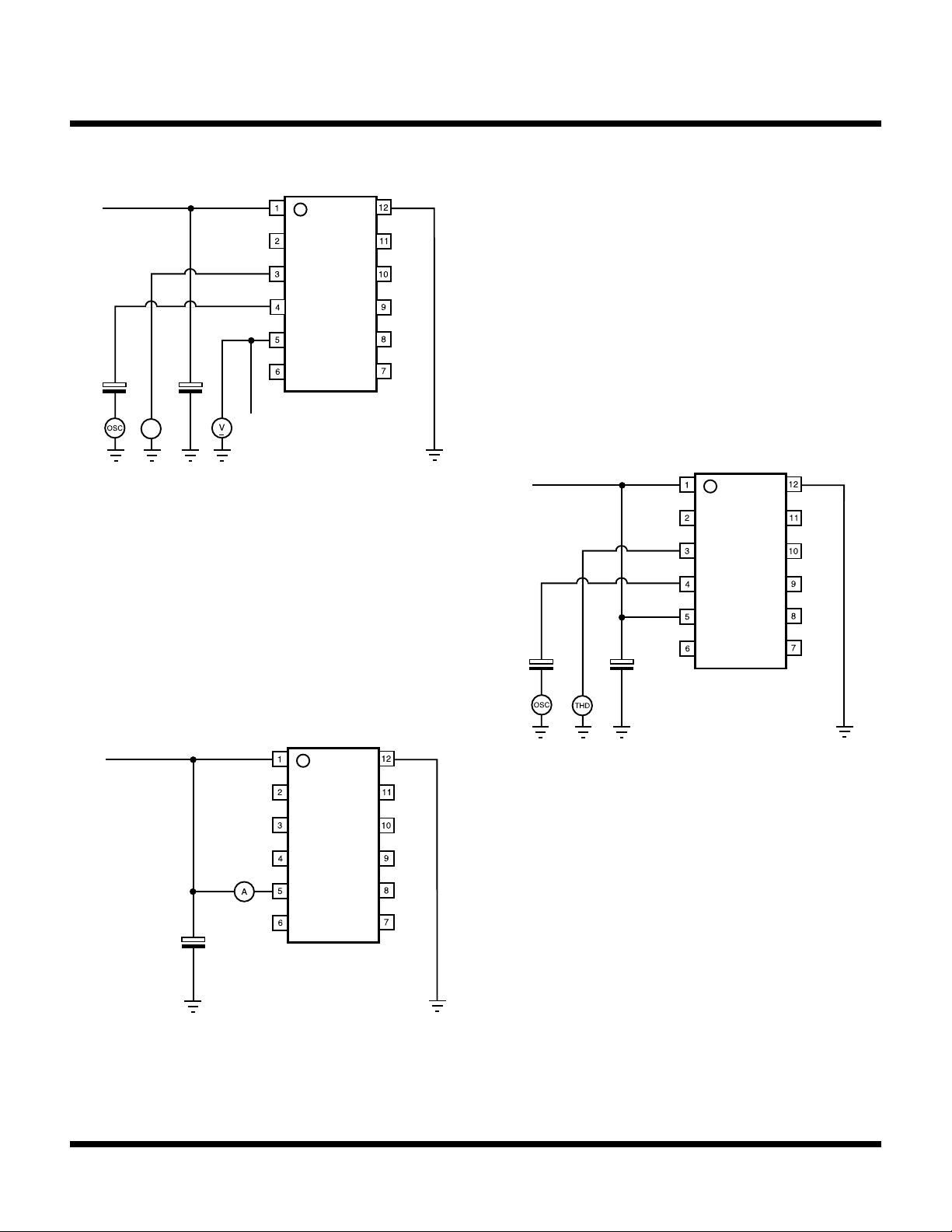
CONTROL INPUT IMPEDANCE (FIGURE 3)
This is the input resistance of control terminals.
1) Measure the inflow current from V
to Pin 5.
CC
2) Calculate:
IMP = VCC / Inflow Current
This resistancde is the input impedance.
TOTAL HARMONIC DISTORTION (FIGURE 4)
Use the lower distortion oscillator for this measurement
because distortion of the TK15327 is very low.
1) Connect VCC to Pin 5, Pin 8 is low level or open.
2) Connect a distortion analyzer to Pin 3.
3) Input the sine wave (1 kHz, 1 Vrms) to Pin 4.
4) Measure the distortion of Pin 3. This value is the
distortion of 1-Ach.
5) Next, reverse conditions at Pin 5 and Pin 8.
6) Input the same sine wave to Pin 2.
7) Measure in the same way. This value is the distortion
of 1-Bch.
V
CC
Figure 4
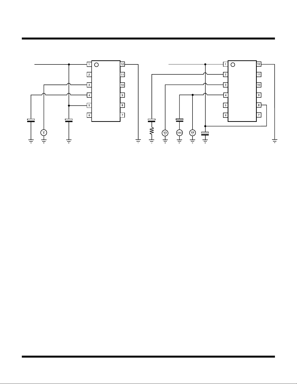
VOLTAGE GAIN (FIGURE 5)
This is the output level against input level.
1) Connect VCC to Pin 5, Pin 8 is low level or open.
2) Connect AC volt meters to Pin 4 and Pin 3.
(Using the same type meter is best)
3) Input a sine wave (f = max. 20 kHz, 1 Vrms) to Pin 4.
+
4) Measure the level of Pin 4 and name this V1.
5) Measure the level of Pin 3 and name this V2.
6) Calculate Gain = 20 Log (( |V2 - V1| )/V1)
V1<V2 + Gain, V1>V2 - Gain
This value is the voltage gain of 1-Ach.
Figure 3
7) Next, reverse conditions at Pin 5 and Pin 8.
8) Input the same sine wave to Pin 2.
9) Measure and calculate in the same way.
This value is the voltage gain of 1-Bch.
Page 4 June 1999 TOKO, Inc.
Page 5
TK15327
V
CC
++
TEST CIRCUITS AND METHODS (CONT.)
V
CC
+
+
Figure 5
MAXIMUM INPUT LEVEL (FIGURE 6)
This measurement measures at output side.
1) Connect VCC to Pin 5, Pin 8 is low level or open.
2) Connect a distortion analyzer and an AC volt meter to
Pin 3.
3) Input a sine wave (1 kHz) to Pin 4 and elevate the voltage
gradually until the distortion gets to 0.1%.
4) When the distortion amounts to 0.1%, stop elevating and
measure the AC level of Pin 3.
This value is the maximum input level of 1-Ach.
5) Next, reverse conditions at Pin 5 and Pin 8.
6) Input the same sine wave to Pin 2.
7) Measure in the same way.
This value is the maximum input level of 1-Bch.
Figure 6
RESIDUAL NOISE (FIGURE 7)
This value is not S/N ratio. This is a noise which occurs from
the device itself.
1) Connect VCC to Pin 5, Pin 8 is low level or open.
2) Connect an AC volt meter to Pin 3.
3) Connect a capacitor from Pin 4 to GND.
4) Measure AC voltage of Pin 3. This value is the noise of
1-Ach. If the influence of noise from outside exists, use
optional filters.
5) Next, reverse conditions at Pin 5 and Pin 8.
6) Connect to GND through a capacitor from Pin 2.
7) Measure in the same way.
This value is the noise level of 1-Bch.
June 1999 TOKO, Inc. Page 5
Page 6
TK15327
V
CC
TEST CIRCUITS AND METHODS (CONT.)
V
CC
++
Figure 7
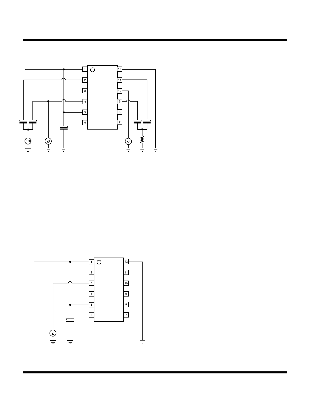
ISOLATION (FIGURE 8)
This is the cross talk between Ach and Bch.
1) Connect VCC to Pin 8, Pin 5 is low level or open.
2) Connect AC volt meters to Pin 4 and Pin 3.
3) Connect a capacitor and a resistance in series to GND
from Pin 2.
4) Input a sine wave (10 kHz, 1 Vrms) to Pin 4.
5) Measure the level of Pin 4 and name this V4.
6) Measure the level of Pin 3 and name this V3.
7) Calculate:
ISO = 20 Log (V3 / V4)
This value is the isolation to Bch from Ach.
8) Next, reverse conditions at Pin 5 and Pin 8.
9) Change line of Pin 2 and Pin 4.
10) Input the same sine wave to Pin 2.
11) Measure and calculate in the same way.
This value is the isolation to Ach from Bch.
+
10 K
+
+
Figure 8
SEPARATION (FIGURE 9)
This is the cross talk between 1ch and 2ch.
1) Connect either Pin 5 or Pin 8 to VCC. One side pin is low
level or open.
2) Connect AC volt meters to Pin 4 (or Pin 2) and Pin 10.
3) Connect Pin 9 and Pin 11 to GND through capacitors
and a resistance.
4) Input a sine wave (10 kHz, 1 Vrms) to Pin 2 and Pin 4.
5) Measure the level of Pin 4 and name this V5.
6) Measure the level of Pin 10 and name this V6.
7) Calculate:
SEP = 20 Log (V6 / V5)
This value is the separation to 2ch from 1ch.
Page 6 June 1999 TOKO, Inc.
Page 7
TEST CIRCUITS AND METHODS (CONT.)
TK15327
V
CC
+ +
+
Figure 9
I/O TERMINAL VOLTAGE (FIGURE 10)
This is the DC voltage of input and output.
Because the input and the output are nearly equal, only the
output is measured.
1) Connect VCC to Pin 5, Pin 8 is low level or open.
2) Connect a DC volt meter to Pin 3 and measure.
This value is the terminal voltage of 1-Ach.
3) Next, reverse conditions at Pin 5 and Pin 8.
4) Measure in the same way.
This value is the terminal voltage of 1-Bch.
OUTPUT TERMINAL DIFFERENCE
This is the DC output voltage difference between Ach and
Bch. This is calculated by using values measured at the
I/O Terminal Voltage.
∆ Vcent = | (1 - Ach value) - (1 - Bch value) |
This value is the voltage difference of 1ch.
+ +
10 K
V
CC
+
Figure 10
June 1999 TOKO, Inc. Page 7
Page 8
TK15327
LEVEL
(dB)
THD
(%)
THD
(%)
LEVEL
(V
)
LEVEL
(dB)
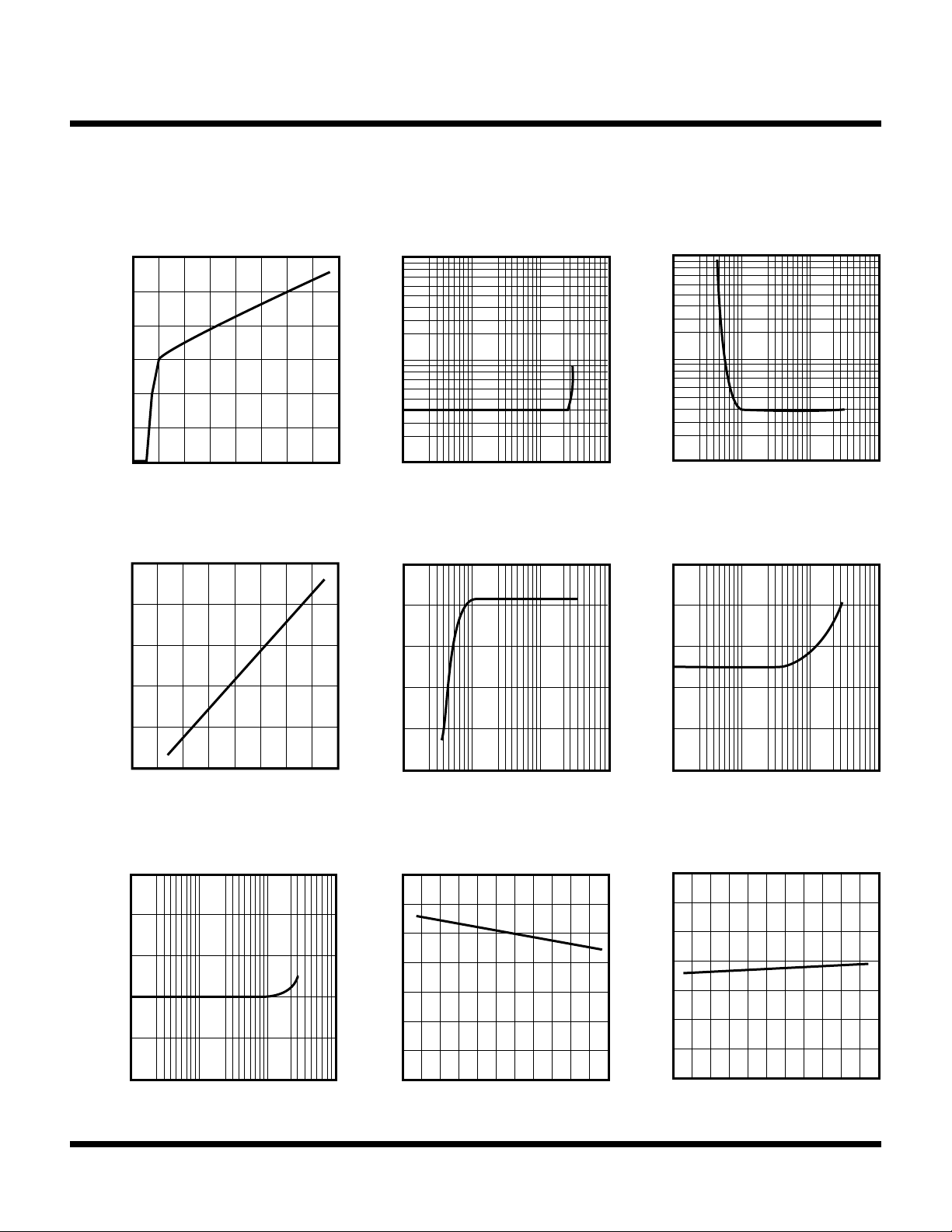
TYPICAL PERFORMANCE CHARACTERISTICS
VCC = 8 V, TA = 25 °C, unless otherwise specified.
SUPPLY CURRENT
6
5
4
(mA)
3
CC
I
2
1
0
0 2 4 6 8 10 12 14 16
5
4
rms
3
SUPPLY VOLTAGE
V
(V)
CC
DYNAMIC RANGE
vs. SUPPLY VOLTAGE
VS.
TOTAL HARMONIC DISTORTION
0.1
0.01
0.001
0.1 1 10 100
2
vs. FREQUENCY
f (kHz)
DYNAMIC RANGE
vs. LOAD RESISTANCE
TOTAL HARMONIC DISTORTION
0.1
0.01
0.001
-60
-70
-80
vs. LOAD RESISTANCE
0.1 1 10 100
RL (kΩ)
ISOLATION
vs. FREQUENCY
2
1
0
0 2 4 6 8 10 12 14 16
VCC (V)
SEPARATION
-60
-70
-80
-90
-100
-110
0.1 1 10 100
vs. FREQUENCY
f (kHz)
1
LEVEL (Vrms)
0
0.1 1 10 100
RL (kΩ)
CONTROL THRESHOLD
TEMPERATURE
1.5
1
LEVEL (V)
0.5
0
-20 0 20 40 60 80
TA (°C)
VS.
-90
-100
-110
0.1 1 10 100
f (kHz)
VOLTAGE GAIN VS.
TEMPERATURE
+.1
0
GVA (dB)
-.1
-20 0 20 40 60 80
TA (°C)
Page 8 June 1999 TOKO, Inc.
Page 9
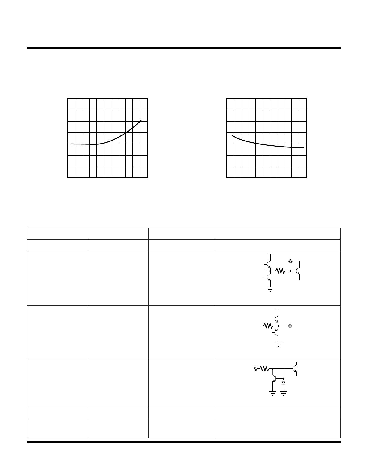
TYPICAL PERFORMANCE CHARACTERISTICS (CONT.)
VCC / 2
65 K
V
= 8 V, TA = 25 °C, unless otherwise specified.
CC
TK15327
RESIDUAL NOISE VS.
TEMPERATURE
6
4
LEVEL (µVrms)
2
0
-20 0 20 40 60 80
TA (°C)
TERMINAL VOLTAGE AND CIRCUIT
Condition: VCC = 8 V.
.ONNIPTNEMNGISSAEGATLOVCDNOITCNUF/TIUCRIC
1V
2
4
9
11
CC
BNI,ANIV4
OUTPUT DIFFERENCE VS.
TEMPERATURE
3
2
LEVEL (mV)
1
0
-20 0 20 40 60 80
TA (°C)
V8niPegatloVylppuS
niPtupnIlangiS
3
01
TUO
8niPdna5niP
100
noitidnoC
emaS
tnereffiD
5
YEKV0
gnitaolF
V4niPtuptuOlangiS
50 K
8
niPlortnoC
21DNGV0niPdnuorG
6
CNgnitaolFniPtcatnoCoN
7
June 1999 TOKO, Inc. Page 9
Page 10
TK15327
1OUT
1BIN V
CC
GND 2BIN
2OUT
1AIN
1KEY 2KEY 2AIN
+
+
10 µF
R
L
10 µF
1Bin
11
10
9
8
7
+
10 µF
+
2 Bin
1Key
2Key
10 µF
+
R
L
10 µF
+
10 µF
+
33 µF
1Ain 2Ain
APPLICATION INFORMATION
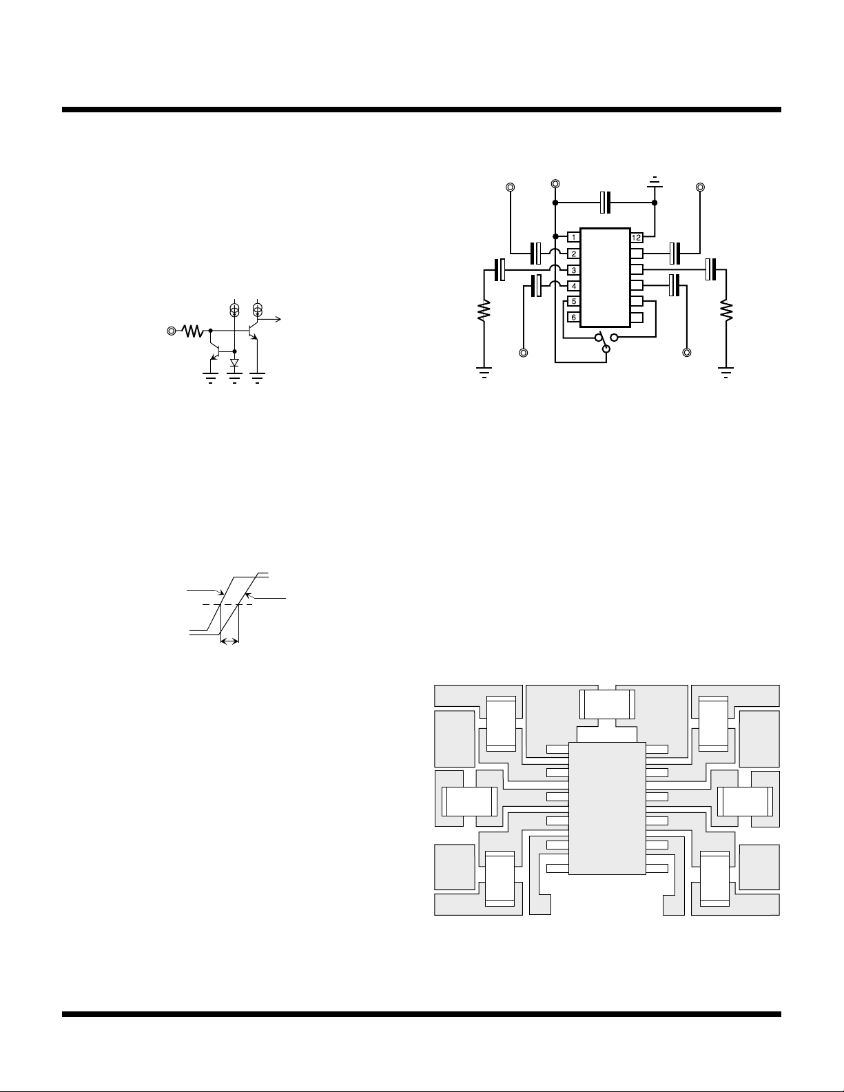
KEY INPUT CIRCUIT
1ch and 2ch is separate action by each control keys. Figure
11 is an equivalence circuit of key input. If two keys are low
level or high level at the same time then the output is floating
condition. (See Terminal DC Voltage and Circuit table on
page 9).
Key in
to Logic
Figure 11
SWITCHING TIME
This time is the signal change response time compared to
the control key input signal. Figure 12 illustrates the timimg
chart. T = 2 µs typically.
Bch (Ach)
Key in
50%
Ach (Bch)
SW out
t
Figure 12
APPLICATION
Figure 13
CROSS TALK (ISOLATION AND SEPARATION)
Figure 14 is an example of a layout pattern. In the
application of the TK15327M, the following must be
considered. Because of the high impedance at the inputs,
the capacitors can act as antennas to each other. If the
parts are bigger, and the space between the capacitors is
too narrow, then cross talk will increase. Therefore, when
designing the printed circuit pattern, separate the input
capacitors as far as possible and use as small a part as
possible (e.g., surface mount types, etc.).
Figure 13 illustrates an example of a typical application.
The standard application is to use capacitor coupling at the
inputs and output of the TK15327M. For characteristics of
distortion and dynamic range versus RL, refer to the graphs
in the Typical Performance Characteristics. The TK15327M
can also be used with direct coupling, but the characteristics will get worse (distortion, etc.). If direct coupling is
desired, then it is recommended to use external circuitry
that is biased compatible with the TK15329M. Input of the
TK15329M is the open base type.
Page 10 June 1999 TOKO, Inc.
Figure 14
Page 11
APPLICATION INFORMATION (CONT.)
11
10
9
8
7
11
10
9
8
7
+
+
+
+
+
+
+
+
+
+
abc d a
b
cd
+
327-1
327-2
1ch-out 2ch-out12 34
control
1ch-in 2ch-in
V
CC
OUTPUT TERMINAL VOLTAGE DIFFERENCE
This parameter is the output voltage difference between
Ach and Bch, and appears when the channel changes from
Ach to Bch, or changes to the reverse. Generally, this is
called Switching Noise or Pop Noise. If this value is big and
if this noise is amplified by the final amplifier and is
outputted by the speakers, then it appears as a Shock
Sound. Output terminal voltage difference of the TK15327M
is a value that adds the internal bias difference and the offset voltage difference. The value of the TK15327M is very
small; its maximum value is 13 mV. Toko can offer the
“Muting IC” if users wish to mute Switching Noise.
DIRECT TOUCH
The signal input terminals:
Internal circuits are operated by constant current circuit,
even if VCC or GND is contacted, damage does not occur.
The signal output terminal:
Outflow or inflow current is decided by ability of final
transistor, but protection circuit is not attached. If GND or
VCC are contacted damage may occur. Pay attention to
long time contact. Do not supply over the maximum rating.
Referenced to GND, do not provide to all terminals over V
+0.3 V or -0.3 V.
DC SIGNAL INPUT
CC
TK15327
Figure 15
KEY NO.
1234
OUTPUT
cHLLL
The output of the TK15327M has a saturation voltage (both
VCC and GND sides about 1.0 V); accordingly the use of a
DC signal is not recommend (e.g., the pulse signal etc.)
NC TERMINAL
NC terminals are not wired inside IC by bonding wire. NC
terminals are not tested so do not connect at outside.
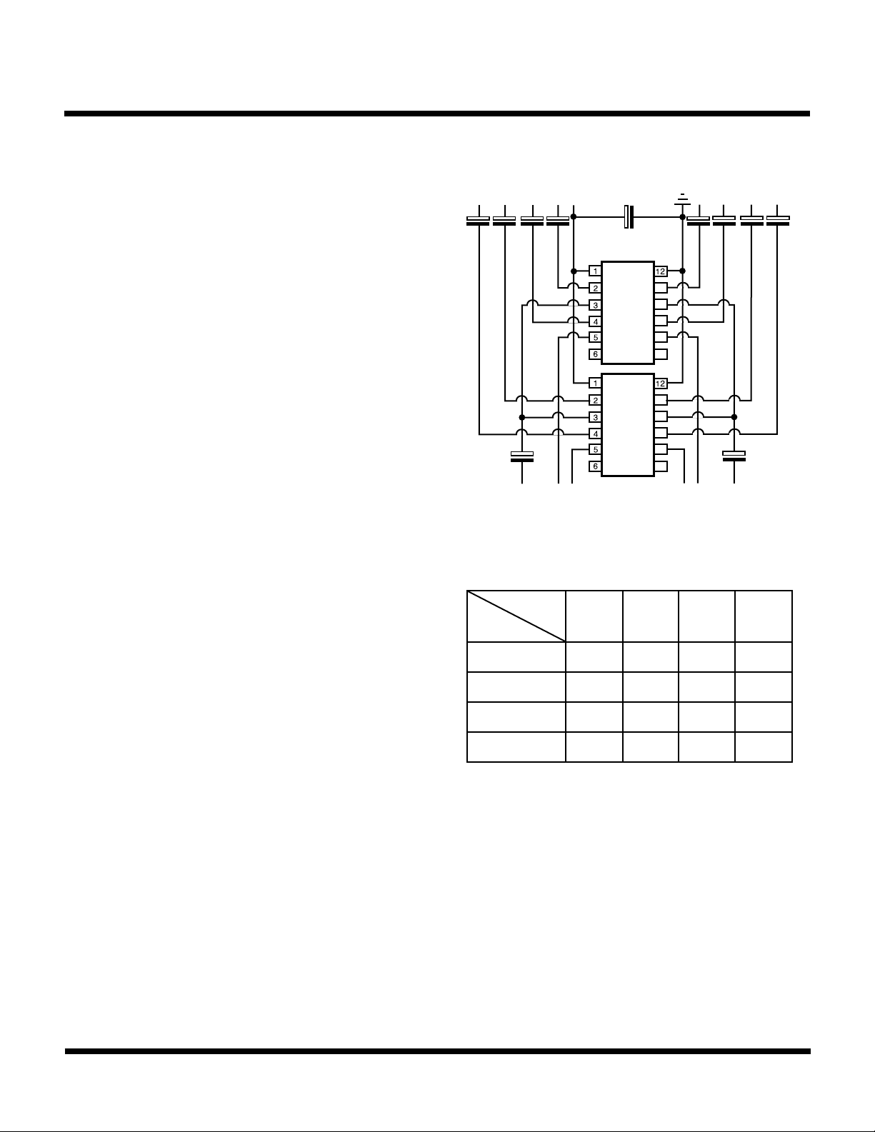
FLOATING POSITION
TK15327 has floating position and can increase optional
channels. Figure 15 is an example to select one output
from four inputs, and the change operates by four controls.
This function is shown in the table below. If channels
increase more, control keys will increase with the same
number too. In this case the Decoder may be necessary.
Each device and channel has individual output voltage
values within a specification. When channels are increased caution the output terminal voltage difference too.
June 1999 TOKO, Inc. Page 11
aLHLL
bLLHL
d LLLH
When all is high level or low level, output is the floating.
Plural high level is prohibited.
Page 12
TK15327
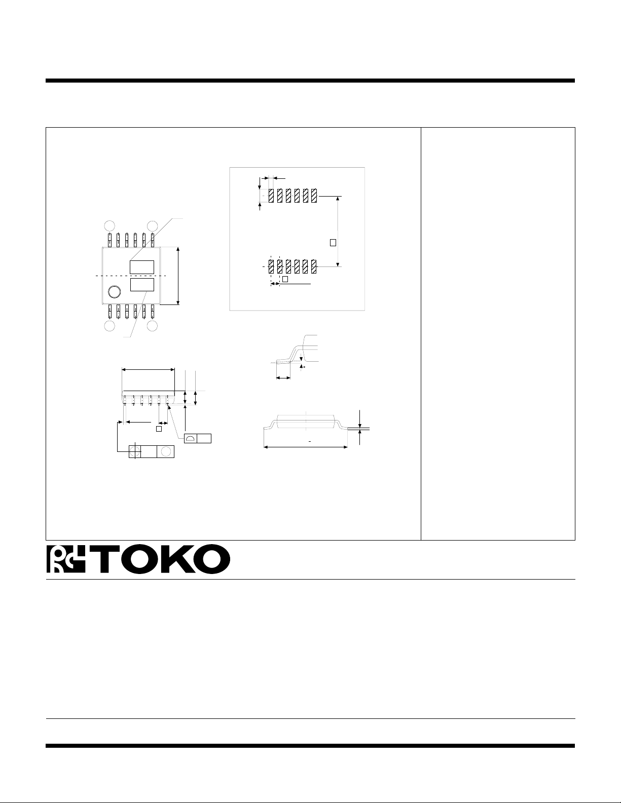
PACKAGE OUTLINE
SSOP-12
12
Lot. No.
AAA
YYY
+0.15
-0.05
0.3
Marking Information
0.4
1.2
7
61
5.0
Marking
5.4
e1
4.4
1.7 max
1.4
0 ~ 0.2
e
0.8
M0.10
0.1
e
0.8
Recommended Mount Pad
0 ~ 10
0.5
+
0.3
6.0
+0.15
-0.15
0.15
TK15327M 327
Dimensions are shown in millimeters
Tolerance: x.x = ± 0.2 mm (unless otherwise specified)
Toko America, Inc. Headquarters
1250 Feehanville Drive, Mount Prospect, Illinois 60056
Tel: (847) 297-0070 Fax: (847) 699-7864
TOKO AMERICA REGIONAL OFFICES
Midwest Regional Office
Toko America, Inc.
1250 Feehanville Drive
Mount Prospect, IL 60056
Tel: (847) 297-0070
Fax: (847) 699-7864
Western Regional Office
Toko America, Inc.
2480 North First Street , Suite 260
San Jose, CA 95131
Tel: (408) 432-8281
Fax: (408) 943-9790
Eastern Regional Office
Toko America, Inc.
107 Mill Plain Road
Danbury, CT 06811
Tel: (203) 748-6871
Fax: (203) 797-1223
Semiconductor Technical Support
Toko Design Center
4755 Forge Road
Colorado Springs, CO 80907
Tel: (719) 528-2200
Fax: (719) 528-2375
Visit our Internet site at http://www.tokoam.com
The information furnished by TOKO, Inc. is believed to be accurate and reliable. However, TOKO reserves the right to make changes or improvements in the design, specification or manufacture of its
products without further notice. TOKO does not assume any liability arising from the application or use of any product or circuit described herein, nor for any infringements of patents or other rights of
third parties which may result from the use of its products. No license is granted by implication or otherwise under any patent or patent rights of TOKO, Inc.
Page 12 June 1999 TOKO, Inc.
All Rights Reserved
IC-119-TK119xx
0798O0.0K
Printed in the USA© 1999 Toko, Inc.
 Loading...