

Page 1
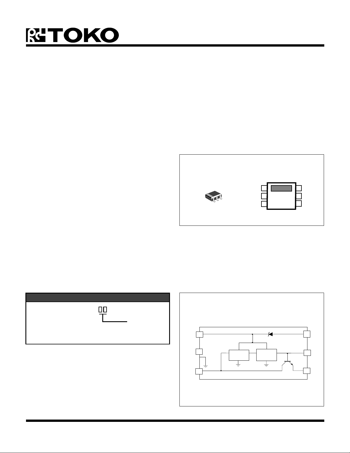
TK11822/11823
1
2
3
4
EMITTER
BASE
DA V
O
6
5
V
IN
GND
E
T
DC-DC CONVERTER
FEATURES
■ Very Low Noise
■ Low Operating Voltage Range
■ Few External Components
■ Wide Supply Voltage Range
■ Sinewave Oscillation
■ Selectable Output Voltages
DESCRIPTION
The TK11822M and TK11823M are booster-type DC-DC
converters developed principally for use as power supplies
to drive variable capacitance diodes. Both products are low
power output types, suitable for operation at low voltages.
To suppress AM band noise, they use high frequency sine
wave oscillation. Both products are available in two output
voltages, allowing the user to select the most efficient
voltage for the equipment. The products have built-in rectifier diodes and small packages, contributing to equipment
miniaturization.
APPLICATIONS
■ Headphone Stereos
■ Pagers
■ Mobile Wireless Equipment
■ Electronic Diaries
■ Other Battery-powered Equipment
■ LCD TV's
TK11822/23M
R3
March 19, 1996 TOKO, Inc.
ORDERING INFORMATION
TK11822M
TK11823M
TAPE/REEL CODE
BX: Bulk/Bag
TL: Tape Left
Tape/Reel Code
V
O
GND 5
VIN 6
BLOCK DIAGRAM
4
Reference
Voltage
Feedback
Control
3 DA
2 BAS
1 EMIT
Page 1
Page 2
TK11822/11823
ABSOLUTE MAXIMUM RATINGS
Input Voltage.............................................................. 8 V
Output Current ..................................................... 0.5 mA
Operating Voltage Range................................. 1.1 to 6 V
Power Dissipation (Note 1) ................................ 200 mW
TK11822 ELECTRICAL CHARACTERISTICS
Test conditions: V
SYMBOL PARAMETER TEST CONDITIONS MIN TYP MAX UNITS
I
CC
V
O
I
O
Line Reg Line Regulation VIN = 1.4 V → 3.6 V, IO = 50 µA2080mV
Load Reg Load Regulation IO = 20 µA → 100 µA 30 100 mV
= 1.4 V, TA = 25 °C, unless otherwise specified.
IN
Input Current
IO = 0 µA 2.1 3.6 mA
IO = 50 µA 3.8 5.6 mA
Output Voltage IO = 50 µA 7.0 7.4 7.8 V
Output Current
VIN = 1.2 V 50 µA
VIN = 1.4 V 150 µA
Junction Temperature .......................................... 150 °C
Storage Temperature Range ...................-55 to +150 °C
Operating Temperature Range .................-20 to +70 °C
Lead Soldering Temp. (10 sec.)...........................260 °C
∆VO/T
A
Output Voltage VIN = 1.4 V → 3.6 V, IO = 50 µA 0.7 mV/°C
Temperature Dependency
V
OSC-S
f
OSC
Note 1: Power dissipation must be derated at the rate of 1.6 mW/°C for operation above 25 °C.
Note 2: Use caution when decreasing the output capacitance at low temperatures. "UJ" type capacitors will allow little change in
the oscillation frequency.
Oscillation Startup Voltage IO = 0 µA 1.0 V
Oscillation Frequency 3.0 MHz
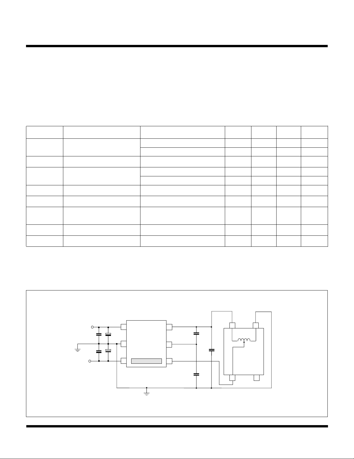
TEST CIRCUIT
GND
V
V
0.1 µF
0.1 µF
IN
O
4
+
5
+
6
3
5 pF
2
8 pF
1
C1
6
1
4
3
Page 2
Toko Inductor: 5CDM-658BN-1085
TK11822 C1 33 pF
TK11823 C1 68 pF
March 19, 1996 TOKO, Inc.
Page 3
TK11822/11823
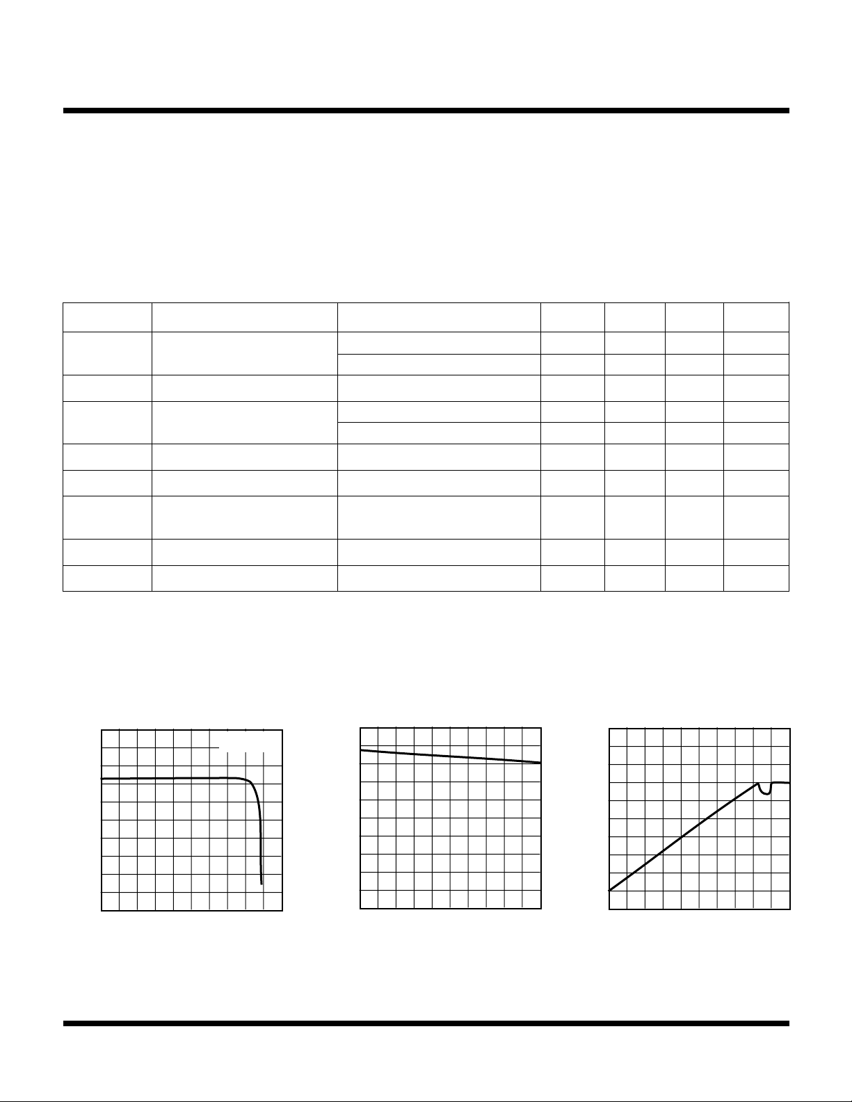
1
OUTPUT VOLTAGE vs.
2
OUTPUT VOLTAGE vs.
3
INPUT CURRENT vs.
ABSOLUTE MAXIMUM RATINGS
Input Voltage .............................................................. 8 V
Output Voltage ......................................................... 18 V
Output Current ..................................................... 0.5 mA
Operating Voltage Range................................. 1.1 to 6 V
Power Dissipation (Note 1) ................................ 200 mW
TK11823 ELECTRICAL CHARACTERISTICS
Test conditions: V
SYMBOL PARAMETER TEST CONDITIONS MIN TYP MAX UNITS
I
CC
= 1.5 V, TA = 25 °C, unless otherwise specified.
IN
Input Current
IO = 0 µA 3.4 5.6 mA
IO = 50 µA 5.4 8.5 mA
Junction Temperature .......................................... 150 °C
Storage Temperature Range ...................-55 to +150 °C
Operating Temperature Range .................-20 to +70 °C
Lead Soldering Temp. (10 sec.)...........................260 °C
V
O
I
O
Output Voltage IO = 50 µA 13.2 13.7 14.2 V
Output Current
VIN = 1.3 V 50 µA
VIN = 1.5 V 150 µA
Line Reg Line Regulation VIN = 1.5 V → 3.6 V, IO = 50 µA2080mV
Load Reg Load Regulation IO = 20 µA → 100 µA 40 110 mV
∆VO/T
A
Output Voltage VIN = 1.5 V → 3.6 V, IO = 50 µA 2.0 mV/°C
Temperature Dependency
V
OSC-S
f
OSC
Oscillation Startup Voltage IO = 0 µA 1.1 V
Oscillation Frequency 3.0 MHz
TYPICAL PERFORMANCE CHARACTERISTICS
TK11822
OUTPUT CURRENT
10
TA = 25 °C
7.5
7.4
OUTPUT CURRENT
25
20
OUTPUT CURRENT
O
5
(V)
V
0
0 100 200 300 400 500
IO (µA)
March 19, 1996 TOKO, Inc.
TPC
7.3
O
(V)
V
7.2
7.1
7.0
0 50 100
IO (µA)
TPC
(mA)
IN
I
15
10
5
0
100 300
0
200
IO (µA)
400
500
TPC
Page 3
Page 4
TK11822/11823
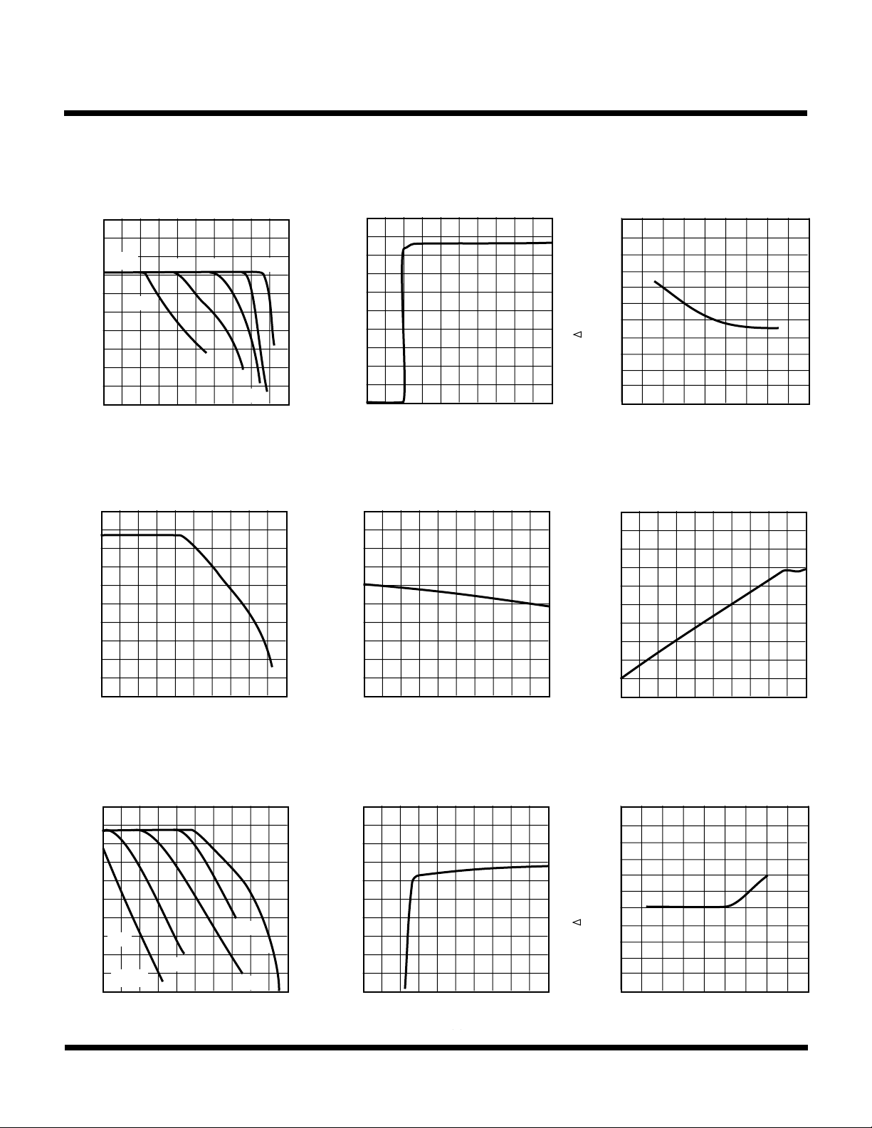
4
OUTPUT VOLTAGE vs. OUTPUT CURRENT
(V)
5
OUTPUT VOLTAGE vs.
V
O
(V)
TEMPERATURE (°C)
TPC6
200
100
0
-100
-200
OUTPUT VOLTAGE vs. TEMPERATURE
-50
0
50
100
7
OUTPUT VOLTAGE vs.
8
OUTPUT VOLTAGE vs.
9
INPUT CURRENT vs.
V
O
(V)
TEMPERATURE (°C)
TPC12
200
100
0
-100
-200
OUTPUT VOLTAGE vs. TEMPERATURE
-50
0
50
100
1
OUTPUT VOLTAGE vs.
OUTPUT VOLTAGE vs. OUTPUT CURRENT
0
TYPICAL PERFORMANCE CHARACTERISTICS (CONT.)
TK11822(CONT.)
AT VARIOUS V
10
V
=
IN
O
5
(V)
V
0
0 100 200 300 400 500
1. 0 V
1.1 V
1.2V
IO (µA)
TK11823
OUTPUT CURRENT
15
O
10
(V)
V
IN
1.4 V
7.5
7.4
7.3
O
(V)
V
INPUT VOLTAGE
7.2
7.1
1.3 V
7.0
0 50 100
VIN
TPC
V
14.0
13.9
13.8
O
13.7
OUTPUT CURRENT
(V)
TPC
(mA)
IN
I
25
OUTPUT CURRENT
20
15
10
5
0 100 200 300 400 500
AT VARIOUS V
15
O
10
(V)
V
1. 0 V
V
=
IN
5
0 100 200 300 400 50
Page 4
IO (µA)
1.1 V
IO (µA)
13.6
13.5
0 50 100
TPC
IN
14.0
IO (µA)
INPUT VOLTAGE
TPC
5
0
100 300
0
200
IO (µA)
400
500
TPC
13.9
13.8
O
(V)
V
1.3 V
1.4 V
1.2V
TPC10
13.7
13.6
13.5
01 5
234
VIN
TPC1
March 19, 1996 TOKO, Inc.
Page 5
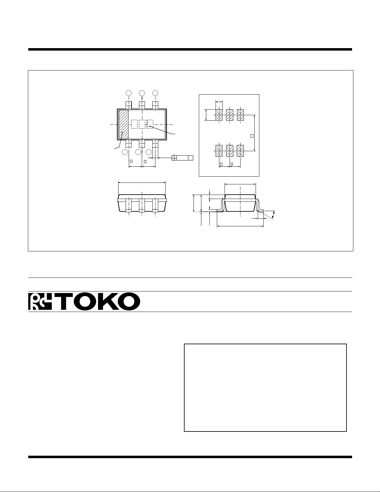
PACKAGE OUTLINES
SOT-23L
456
0.6
1.0
TK11822/11823
3.2
1
e
0.2
±
2.2
±0.15
0.4
0.3
±
3.3
Unit:mm
30° Max
Orientation Mark
1 2 3
e
0.95
±
3.4
Marking
Information
+0.1
-0.05
0.4
e
0.95
0.2
M
0.1
0.2
+0.15
- 0
±
1.2
1.25
0.05
±
0.05
e
e
0.95
0.95
Recommended Mount Pad
0.3
+0.1
-0.05
0.15
MARKING INFORMATION
TK11822 D22
TK11823 D23
The information furnished by TOKO, Inc. is believed to be accurate and reliable. However, TOKO reserves the right to make changes or improvements in the design, specification or manufacture of its products without further notice. TOKO
does not assume any liability arising from the application or use of any product or circuit described herein, nor for any infringements of patents or other rights of third parties which may result from the use of its products. No license is granted
by implication or otherwise under any patent or patent rights of TOKO, Inc.
TOKO America, Inc.
1250 Feehanville, Dr.
Mt. Prospect, IL 60056
Tel: (800) PIK-TOKO
Fax: (847) 699-1194
March 19, 1996 TOKO, Inc.
© 1993 Toko America, Inc.
All Rights Reserved
YOUR LOCAL REPRESENTATIVE IS:
Page 5
Printed in U.S.A.Order this literature by: IC-109-TK11821
 Loading...