

Page 1
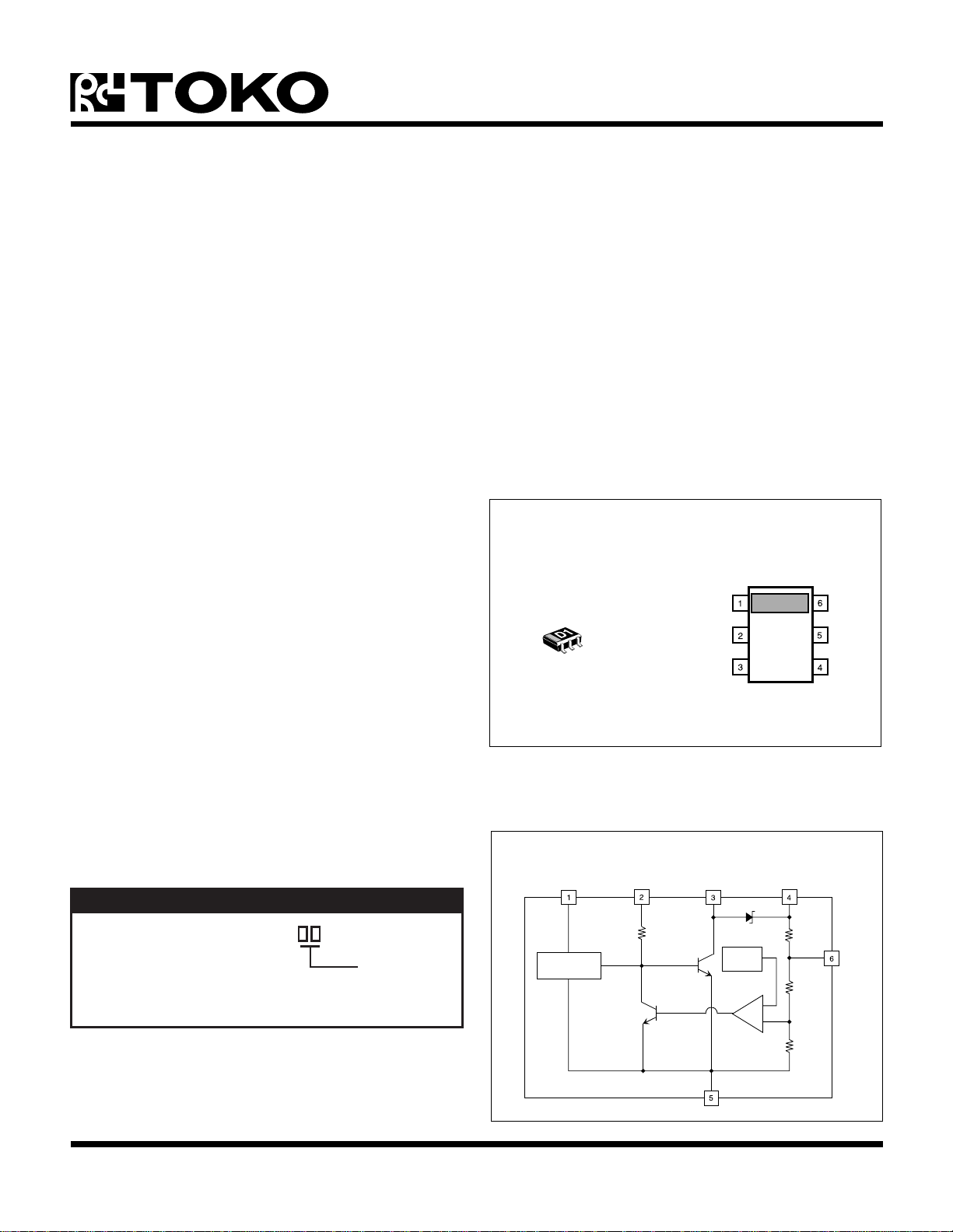
TK11811
20P
DC-DC CONVERTER
FEATURES
■ Miniature Package (SOT-23L)
■ Low Start-up Voltage [0.6 V (typ.)]
■ Few External Components
■ Selectable Output Voltage (1.9 V or 2.8 V)
■ High and Low Current Optimized Designs
DESCRIPTION
The TK11811 is a low power, low input voltage DC-DC
converter.
This device can be optimized for use in high or low current
applications through component selection. The output
voltage is selectable for 1.9 or 2.8 V operation and can be
trimmed to any voltage in between.
The frequency of the built-in relaxation oscillator is set by
external components. The internal voltage regulator
provides a stable output voltage. Optimized Toko inductor
components are available.
APPLICATIONS
■ Pagers
■ Cassette Recorders
■ Cordless Telephones
■ Portable Instrumentation
■ Radio Control Systems
■ Mobile Radios
■ Battery Operated Equipment
■ Local Area Network (LAN) Receivers
TK11811
V
IN
F
B
OSC
T
GND
V
OUT
The TK11811 is available in a miniature SOT-23L surface
mount package.
BLOCK DIAGRAM
V
IN
F
B
OSC V
OUT
ORDERING INFORMATION
TK11811M
V
Tape/Reel Code
TAPE/REEL CODE
TL: Tape Left
OSCILLATOR
ref
-
+
GND
January 1999 TOKO, Inc. Page 1
T
Page 2
TK11811
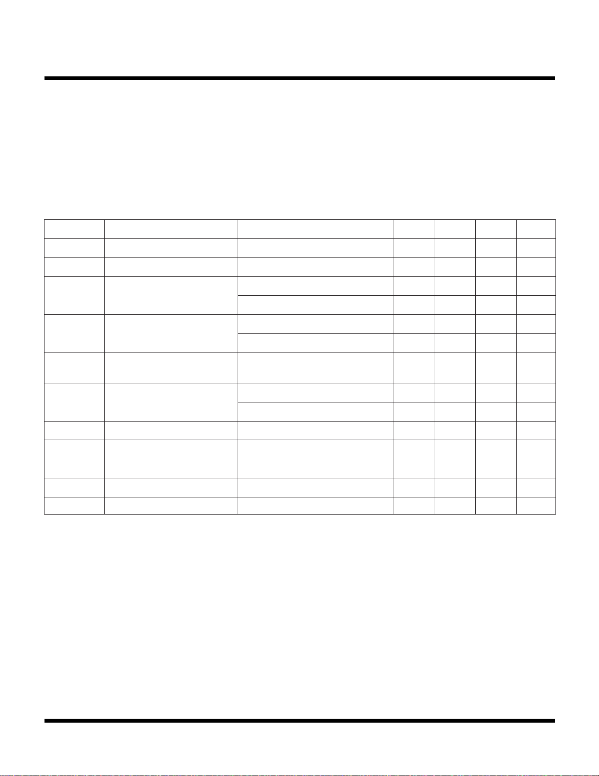
ABSOLUTE MAXIMUM RATINGS
Input Voltage ............................................................ 16 V
Power Dissipation (Note 1) ................................ 200 mW
Junction Temperature ........................................... 150 °C
TK11811 ELECTRICAL CHARACTERISTICS
Test Conditions: TA = 25 °C, V
LOBMYSRETEMARAPSNOITIDNOCTSETNIMPYTXAMSTINU
= 2.9 V (V
OUT
to T open), unless otherwise specified.
OUT
Storage Temperature Range ................... -55 to +150 °C
Operating Temperature Range ...................-10 to +65 °C
Lead Soldering Temperature (10 s) ...................... 235 °C
V
NI
V
TRATS
I
NI
V
TUO
V
I
)WOL(TUO
TUO
tnerruCtupnI
egatloVtuptuO
tnerruCtuptuO
geReniLnoitalugeReniLI
geRdaoLnoitalugeRdaoLV
FFEycneiciffEV
F
CSO
∆V
/∆T
TUO
Note 1: Power dissipation is 400 mW when mounted as recommended. Derate at 3.2 mW/°C for operation above 25 °C. Power dissipation is
Note 2: This IC is a frequency-controlled DC-DC converter; thus the value is varied by condition.
200 mW when in Free Air. Derate at 1.6 mW/°C for operation above 25 °C.
egnaRegatloVylppuS 6.041V
egatloVpu-tratSI
)WOL(egatloVtuptuO
ycneuqerFrotallicsOV
tneiciffeoCerutarepmeTV
TUO
V
NI
V
NI
V
NI
V
NI
V
NI
V
NI
V
NI
TUO
NI
NI
NI
NI
Am0=6.057.0V
I,V1.1=
TUO
I,V4.1=
TUO
I,V1.1=
TUO
I,V4.1=
TUO
I,V1.1=
VotT
TUO
TUO
Am3=0.11Am
Am3=3.8Am
Am3=58.2V
Am3=07.258.20.3V
,Am3=
detcennoc
57.109.150.2V
V1.1=0.45.4Am
V4.1=0.68.6Am
V1.1,Am3= ≤ VNI≤ V0.201Vm
Am5.0,V1.1= ≤ I
I,V4.1=
TUO
I,V4.1=
TUO
I,V4.1=
TUO
≤ Am354Vm
TUO
Am3=3627%
)2etoN(,Am3=003zHk
Am3=7.0C°/Vm
Page 2 January 1999 TOKO, Inc.
Page 3
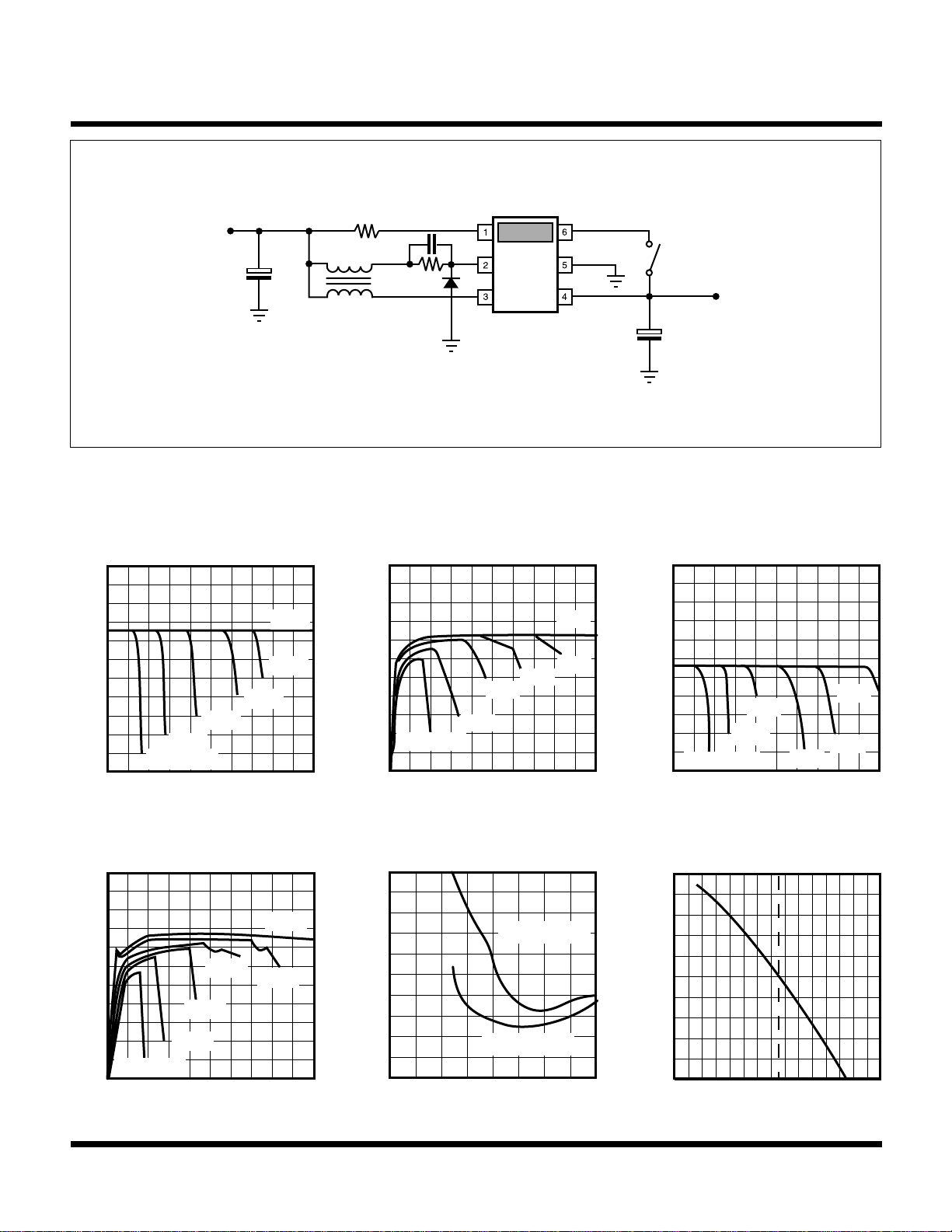
TEST CIRCUIT
R
1
V
IN
C
10 µF
10 KΩ
C2 3300 pF
+
1
L
13
R
2
46
22 KΩ
V
IN
F
B
Di
OSC
T
GND
V
OUT
Note: Di: IS2837,38 (NEC)
L: Toko 395KN-0369AQ
Toko PS5CDL-1639X
TYPICAL PERFORMANCE CHARACTERISTICS
TA = 25°C, unless otherwise specified.
TK11811
(See “Voltage
Adjustment Circuit”)
V
OUT
+
C
3
10 µF
OUTPUT VOLTAGE VS. OUTPUT
CURRENT (V
OUT
= 1.9 V)
2.5
2.0
(V)
1.5
OUT
V
1.0
1.0 V
.5
0
0 2 4 6 8 10
0.8 V
V
= 0.6 V
IN
I
OUT
EFFICIENCY
CURRENT (V
(mA)
VS.
OUT
OUTPUT
= 2.8 V)
100
1.2 V
50
EFF (%)
1.0 V
1.2 V
1.4 V
1.6 V
1.4 V
1.6 V
EFFICIENCY VS. OUTPUT CURRENT
(V
= 1.9 V)
OUT
100
50
EFF (%)
1.0 V
0.8 V
VIN = 0.6 V
0
0 5 10
I
(mA)
OUT
INPUT CURRENT
VOLTAGE (I
200
OUT
V
OUT
(µA)
IN
I
1.2 V
VS.
INPUT
= 0 mA)
= 2.8 V
1.6 V
1.4 V
OUTPUT VOLTAGE
CURRENT (V
OUT
VS.
= 2.8 V, I
5
4
(V)
3
OUT
V
2
1
VIN = 0.6 V
0
.5 5 10
1.0 V
0.8 V
1.2 V
I
(mA)
OUT
OUTPUT VOLTAGE DRIFT
VS. TEMPERATURE
+50
(mV)
0
OUT
∆V
OUTPUT
= 0 mA)
LOAD
1.6 V
1.4 V
0.8 V
V
= 0.6 V
IN
0
0 5 10
I
(mA)
OUT
100
V
OUT
= 1.9 V
0 10 20
VIN (V)
-50
-50 0 50 100
TA (°C)
January 1999 TOKO, Inc. Page 3
Page 4
TK11811
INPUT CURRENT VS. INPUT
VOLTAGE (I
OUT
= 0 mA)
0 10 20
VIN (V)
0
I
IN
(µA)
100
200
V
OUT
= 1.9 V
V
OUT
= 2.8 V
V
(V)
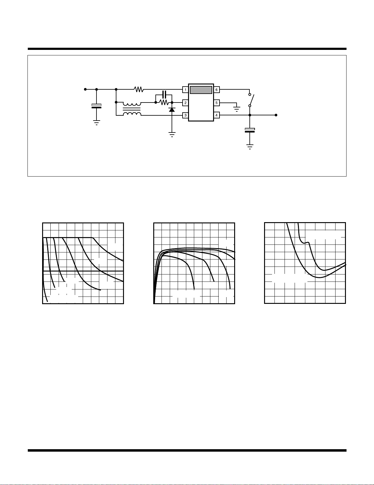
TEST CIRCUIT
R
1
V
IN
C
10 µF
10 KΩ
C2 3300 pF
+
1
L
13
R
2
46
22 KΩ
V
IN
F
B
Di
OSC
T
GND
V
OUT
+
Note: L: Toko 395KN-0370UG
Note: This test circuit is effective at low load current.
TYPICAL PERFORMANCE CHARACTERISTICS
TA = 25°C, unless otherwise specified.
C
10 µF
(See “Voltage
Adjustment Circuit”)
V
OUT
3
OUTPUT VOLTAGE
OUTPUT CURRENT
3
2
OUT
1.0 V
0.8 V
V
= 0.6 V
IN
1
0 1 2 3 4 5
I
(mA)
OUT
1.4 V
1.2 V
VS.
1.6 V
EFFICIENCY
VS.
OUTPUT
CURRENT
100
50
EFF (%)
1.0 V
VIN = 0.8 V
0
0 1 2 3 4 5
I
(mA)
OUT
1.6 V
1.4 V
1.2 V
Page 4 January 1999 TOKO, Inc.
Page 5
TK11811
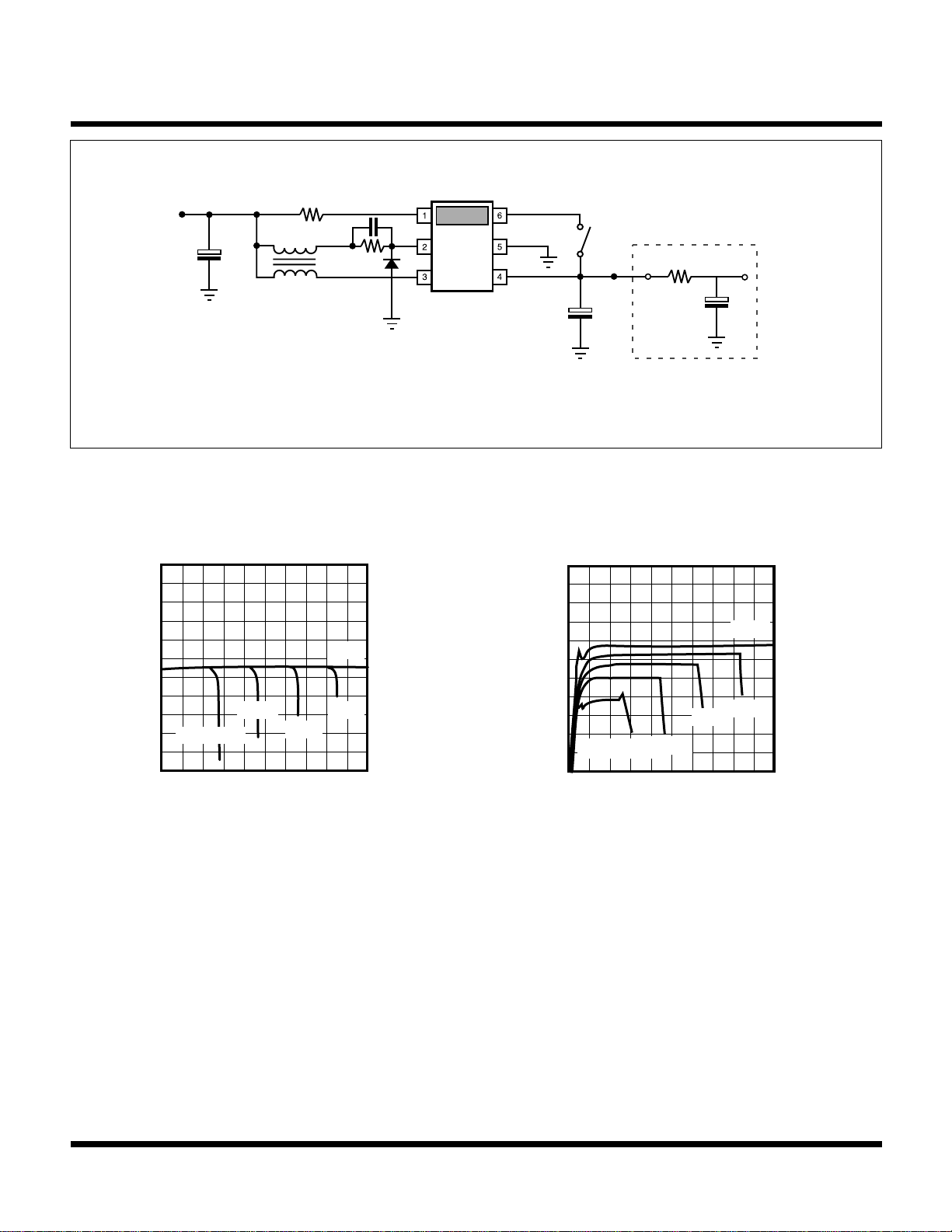
TEST CIRCUIT
R
1
V
IN
C
10 µF
+
1
10 KΩ
C2 0.1 µF
13
L
46
R
22 KΩ
2
L: Toko 395KN-0369AQ
Note: This test circuit is effective at high load currents. By changing C2 from 3300pF to 0.1 µF, the converter operates in the burst mode. The apparent
frequency of operation drops (70 to 100 kHz) and a larger output ripple occurs during burst mode operation. A ripple filter consisting of Cf and Rf can
be added to the output to reduce noise. The values of C
voltage will drop slightly due to Rf.
TYPICAL PERFORMANCE CHARACTERISTICS
TA = 25°C, unless otherwise specified.
V
IN
F
B
Di
OSC
and Rf should be determined experimentally based on the design parameters. The output
f
T
GND
OUT
RIPPLE FILTER
R
V
OUTV
+
C
3
10 µF
f
+
C
f
OUTPUT VOLTAGE
OUTPUT CURRENT
5
4
(V)
3
OUT
V
2
0.8 V
VIN = 0.6 V
1
0
0 2 4 6 8 10
I
OUT
1.0 V
(mA)
VS
.
1.4 V
1.2 V
EFFICIENCY
VS.
OUTPUT
CURRENT
100
50
EFF (%)
1.0 V
I
OUT
0.8 V
(mA)
VIN = 0.6 V
0
0 5 10
1.4 V
1.2 V
January 1999 TOKO, Inc. Page 5
Page 6
TK11811
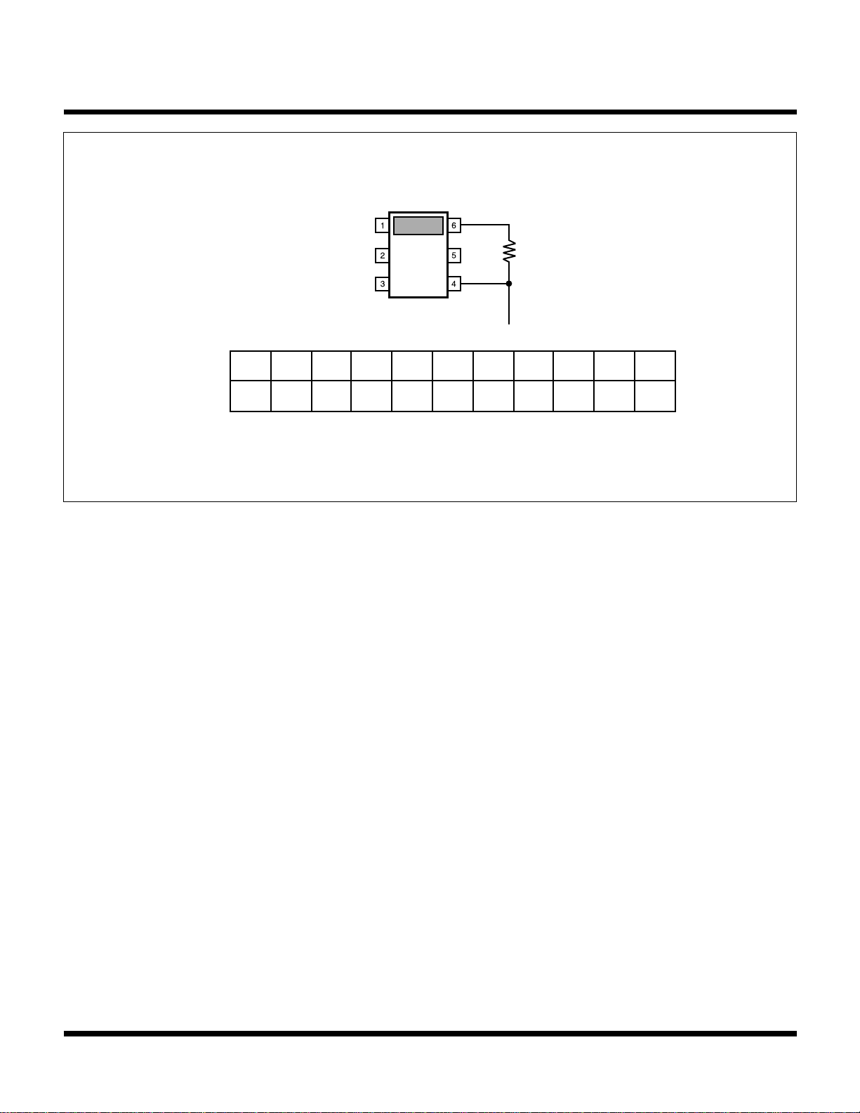
VOL TAGE ADJUSTMENT CIRCUIT
T
R
V
OUT
V
Note: The output voltage can be set between 1.9 V and 2.8 V with an external resistor connected between pins 4 and 6.
1.9 2.0 2.1 2.2 2.3 2.4 2.5 2.6 2.7 2.8
OUT
R 0 12 k 22 k 33 k 56 k 82 k 150 k 330 k 560 k *
ADDITIONAL INFORMATION
APPLICATION INFORMATION
Maximize copper foil area connecting to all IC pins for
optimum performance. Place input and output bypass
capacitors close to the GND pin. For best transient behavior
and lowest output impedance use as large a capacitor
value as possible. The temperature coefficient of the
capacitance and Equivalent Series Resistant (ESR) should
be taken into account. These parameters can influence
power supply noise and ripple rejection. In extreme cases,
oscillation may occur. In order to maintain stability, the
output bypass capacitor value should be minimum 10 µF
in case of tantalum electrolytic or 15 µF in case of aluminum
electrolytic.
HANDLING MOLDED RESIN PACKAGES
All plastic molded packages absorb some moisture from
the air. If moisture absorption occurs prior to soldering the
device into the printed circuit board, increased separation
of the lead from the plastic molding may occur, degrading
the moisture barrier characteristics of the device. This
property of plastic molding compounds should not be
overlooked, particularly in the case of very small packages
where the plastic is very thin. In order to preserve the
original moisture barrier properties of the package, devices
are stored and shipped in moisture proof bags filled with
dry air. The bags should not be opened or damaged prior
to actual use of the devices. If this is unavoidable, the
devices should be stored in a low relative humidity
environment (40 to 65 %) or in an enclosed environment
with desiccant.
INDUCTOR NOTES
The output current and efficiency are largely dependant
upon the coil used. A coil with lower DC resistance is
generally better in efficiency than one with a higher DCR
(DC Resistance). The recommended TOKO 395KN-0369
AQ is 1:1 turns ratio transformer with an inductance of
110 µH and Toko 395KN-0370UG is 1:3 turns ratio
transformer with inductance of 60 µH:600 µH. These coils,
or equivalent, should be used. Smaller coils with higher
DCR will not perform as well as the above coil, and the
oscillator will not be stable.
FEEDBACK RC TIME CONSTANT
If a different coil is used other than the one mentioned, the
RC time constant of the feedback loop will need to be
adjusted for optimum performance. Generally, a lower
resistance will give more output current. In fact, R can be
zero; however, lower resistance will sacrifice efficiency at
low output currents as the quiescent current increases. If
the capacitance is increased beyond or below a certain
value, the oscillator will become unstable. The optimum
Page 6 January 1999 TOKO, Inc.
Page 7

ADDITIONAL INFORMATION (CONT.)
RC values depend upon the operating current, and should
be chosen experimentally using the given values of 3300
pF and 22 kΩ as a starting point.
INPUT/OUTPUT DECOUPLING CAPACITORS
DC-DC converters generate a large ripple current on both
the input and the output of the circuit. The capacitors used
should be as large as possible and have low impedance in
the 300 kHz range. Since low temperatures cause
capacitors to decrease capacitance and increase
Equivalent Series Resistance (ESR), care should be taken
to choose capacitors that have acceptable characteristics
over the temperature range you intend to use. This should
be done experimentally to verify results, as capacitor
performance varies widely from manufacturer to
manufacturer. Tantalum capacitors are generally the best
choice and 10 µF should be adequate for most applications.
LOAD CHARACTERISTICS
TK11811
The TK11811 should not be allowed to start-up under full
load conditions. If this occurs, the output may not stabilize
to the correct output voltage. This can be compensated for,
somewhat, by adjusting the RC of the feedback loop or by
decreasing the output decoupling capacitor. Maximum
current can be drawn after the oscillator has started and
the output has reached nominal output voltage. This is
more critical with input voltages under 1.3 V as the converter
needs to generate sufficient output to ensure correct
internal bandgap and bias voltages.
January 1999 TOKO, Inc. Page 7
Page 8
TK11811
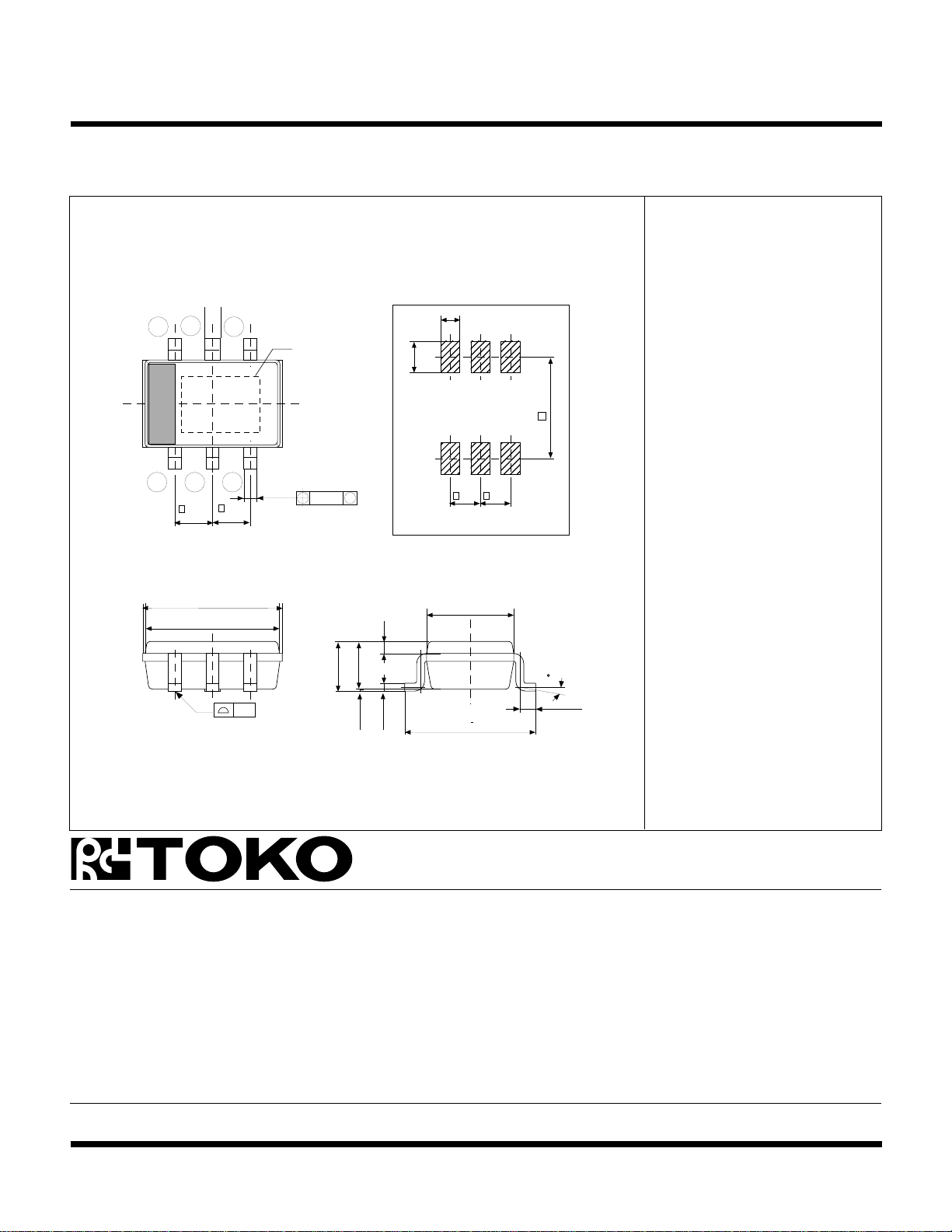
PACKAGE OUTLINE
SOT-23L (SOT-23L-6)
456
123
e e
0.95 0.95
+0.3
- 0.1
3.5
(3.4)
0.1
Dimensions are shown in millimeters
Tolerance: x.x = ± 0.2 mm (unless otherwise specified)
0.32
+0.15
- 0.05
Marking
Marking Information
Marking
TK11811 D1
0.6
1.0
3.0
e1
0.1
M
Recommended Mount Pad
0.3
1.2
1.4 max
+0.15
- 0.05
0 - 0.1
0.15
ee
0.95 0.95
2.2
+ 0.3
3.3
15 max
0.4
Toko America, Inc. Headquarters
1250 Feehanville Drive, Mount Prospect, Illinois 60056
Tel: (847) 297-0070 Fax: (847) 699-7864
TOKO AMERICA REGIONAL OFFICES
Midwest Regional Office
Toko America, Inc.
1250 Feehanville Drive
Mount Prospect, IL 60056
Tel: (847) 297-0070
Fax: (847) 699-7864
Western Regional Office
Toko America, Inc.
2480 North First Street , Suite 260
San Jose, CA 95131
Tel: (408) 432-8281
Fax: (408) 943-9790
Eastern Regional Office
Toko America, Inc.
107 Mill Plain Road
Danbury, CT 06811
Tel: (203) 748-6871
Fax: (203) 797-1223
Semiconductor Technical Support
Toko Design Center
4755 Forge Road
Colorado Springs, CO 80907
Tel: (719) 528-2200
Fax: (719) 528-2375
Visit our Internet site at http://www.tokoam.com
The information furnished by TOKO, Inc. is believed to be accurate and reliable. However, TOKO reserves the right to make changes or improvements in the design, specification or manufacture of its
products without further notice. TOKO does not assume any liability arising from the application or use of any product or circuit described herein, nor for any infringements of patents or other rights of
third parties which may result from the use of its products. No license is granted by implication or otherwise under any patent or patent rights of TOKO, Inc.
Page 8 January 1999 TOKO, Inc.
All Rights Reserved
IC-134-TK11811
0798O0.0K
Printed in the USA© 1999 Toko, Inc.
 Loading...