

Page 1
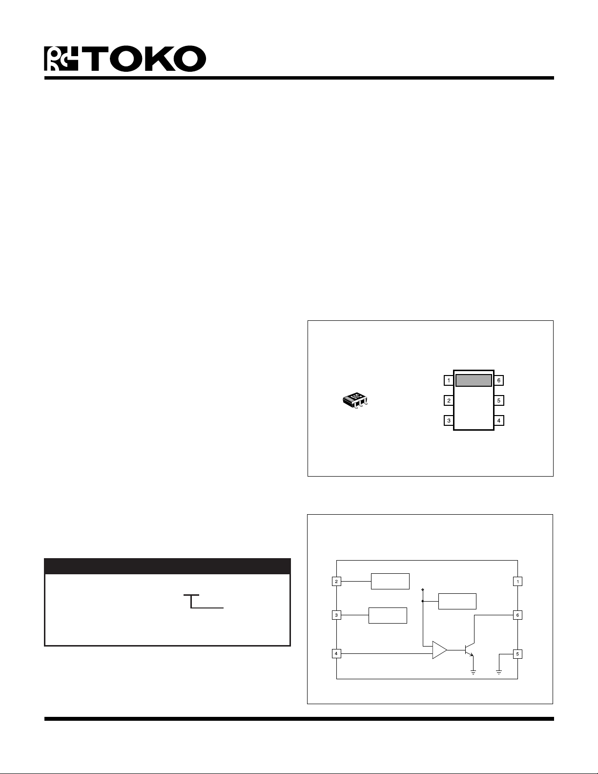
TK11051
01S
TEMPERATURE CONTROLLER IC
FEATURES
■ Internal Temperature Sensor, Voltage Reference
and Comparator
■ Temperature Threshold and Hysteresis Set by Only
Two External Resistors
■ Output Logic: High to Low with Increasing Temp.
■ Active High On/Off Control
■ 2.7 to 6.0 V Supply Range
■ Miniature Package (SOT-23L-6)
■ Minimum External Parts Count
■ Low Power Consumption
■ Very Wide Temperature Range
DESCRIPTION
The TK11051 is an accurate temperature controller IC for
use over the -30 to +105 °C temperature range. The
TK11051 monolithic bipolar integrated circuit contains a
temperature sensor, stable voltage reference and a
comparator, making the device very useful as an on/off
temperature controller. Two external resistors easily set
the sensing temperature threshold and hysteresis. Its wide
operating voltage range of 2.7 to 6.0 V makes this IC
suitable for a number of applications requiring accurate
temperature control. The device is in the “on” state when
the control pin is pulled to a logic high level.
APPLICATIONS
■ Home and Industrial Thermostats
■ Home Appliance Temperature Control
■ Notebook Computer Temperature Monitor
■ Pentium Processor Temperature Monitor
■ Power Supply Overtemperature Protection
■ Copy Machine Overtemperature Protection
■ System Overtemperature Protection
TK11051
V
CONT
V
CC
V
REF
COMP OUT
GND
COMP IN
The TK11051 is available in a miniature SOT-23L-6 surface
mount package.
BLOCK DIAGRAM
ORDERING INFORMATION
V
CONT
TK11051MTL
Tape/Reel Code
TAPE/REEL CODE
TL: Tape Left
January 1999 TOKO, Inc. Page 1
V
REF
COMP IN
ON/OFF
CIRCUIT
VOLTAGE
REFERENCE
V
PTAT
+
-
TEMPERATURE
SENSOR
V
CC
COMP OUT
GND
Page 2
TK11051
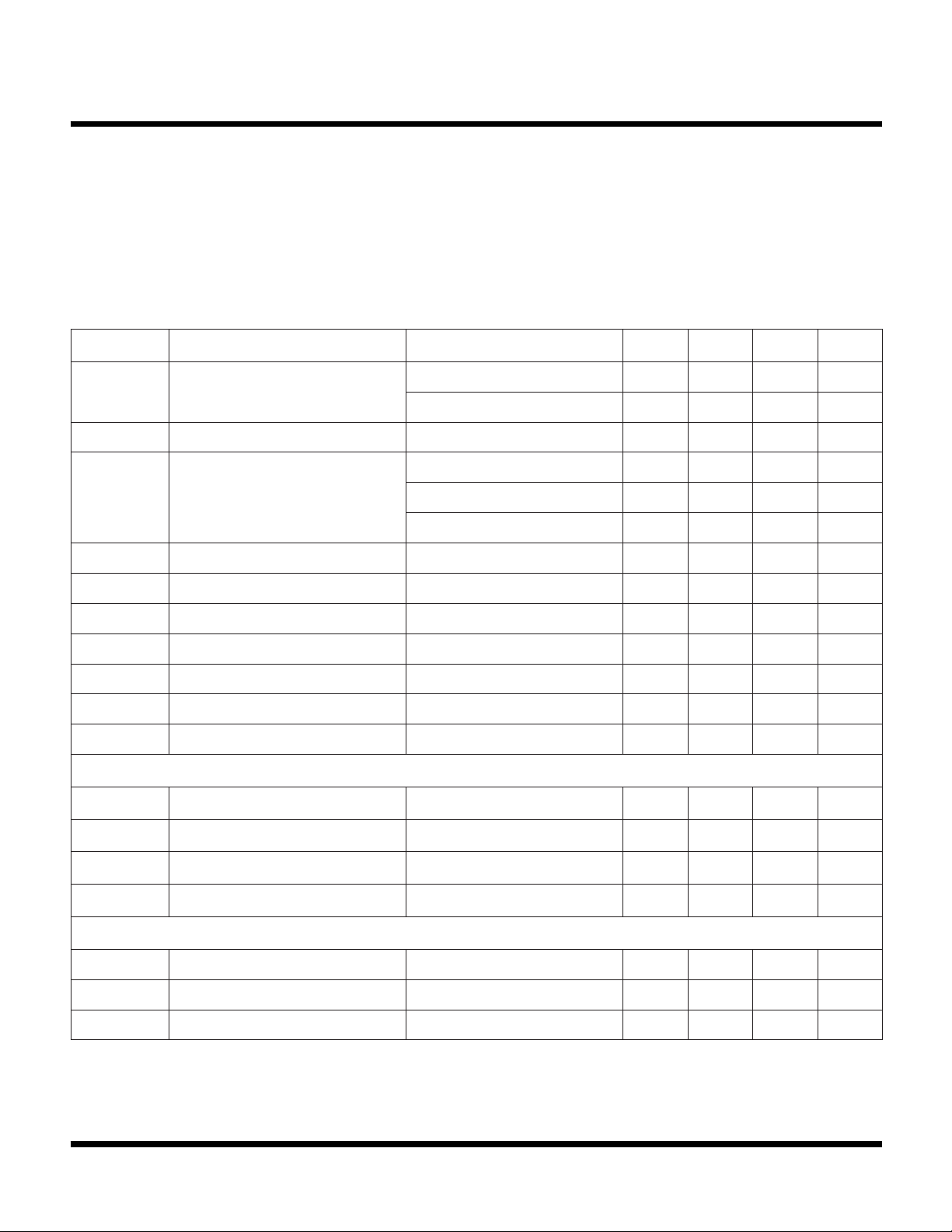
ABSOLUTE MAXIMUM RATINGS
Supply Voltage ......................................................... 12 V
Power Dissipation (Note 1) ................................ 200 mW
Storage Temperature Range ................... -55 to +150 °C
Operating Temperature Range .................-30 to +105 °C
TK11050 ELECTRICAL CHARACTERISTICS
Test conditions: TA = 25 °C, V
LOBMYSRETEMARAPSNOITIDNOCTSETNIMPYTXAMSTINU
= 3.0 V, V
CC
CONT
= 2.4 V, I
Operating Voltage Range................................. 2.7 to 6 V
Junction Temperature .......................................... 150 °C
Lead Soldering Temperature (10 s) ..................... 235 °C
= 40 µA, R3 = 100 kΩ, unless otherwise specified.
OUT
I
CC
I
YBTS
V
TATP
T
C
T
RRE
C
HL
C
LL
I
BI
I
HS
I
TUO
V
fer
V
fer
)4etoN(
tnerruCtnecseiuQ
HGIHtuptuOrotarapmoC012053Aµ
tnerruCybdnatSV
egatloVrosneSerutarepmeT
tneiciffeoCerutarepmeTT
rorrEerutarepmeTT
≤ V6.01Aµ
TNOC
T
A
T
A
T
A
A
A
C°52=291.1V
C°58=234.1V
C°03-=279.0V
C°58ot0=0.4C°/Vm
)2etoN(,C°58ot0=0.4-00.4C°
HGIHtuptuOrotarapmoC)3etoN(8.2V
WOLtuptuOrotarapmoCR
tnerruCsaiBtupnIV>NIrotarapmoC
tnerruCteSsiseretsyHV<NIrotarapmoC
tnerruCkniStuptuOC
≥ k01 Ω )3etoN(,3.0V
3
TATP
TATP
≤ V3.003003Aµ
LL
SCITSIRETCARAHCLANIMRET
egatloVecnerefeRT
A
C°52=6.1V
1.03.0Aµ
9.052.16.1Aµ
WOLtuptuOrotarapmoC052053Aµ
I
fer
geReniLnoitalugeReniLV
geRdaoLnoitalugeRdaoLI
tnerruCtuptuOecnerefeRR
1R+2
CC
TUO
k04= Ω 04005Aµ
V6ot3=28Vm
Aµ005ot0=18Vm
SNOITACIFICEPSLANIMRETLORTNOC
I
TNOC
V
V
Note 1: Power dissipation is 200 mW when in Free Air. Derate at 1.6 mW/°C for operation above 25 °C.
Note 2: The resistance values of R1 and R2 can be calculated as follows: R1 = V
Note 3: When V
Note 4: V
)NO(TNOC
)FFO(TNOC
R1 x IIB - T
PTAT
SET x TC). IIB
< COMP IN, COMP OUT > 2.8 V (High Level). When V
PTAT
does not have an output pin.
tnerruClortnoC15.36Aµ
)NO(egatloVlortnoCNOtuptuO8.1V
)FFO(egatloVlortnoCFFOtuptuODNG6.0V
x T
/ (T
is 0.1 µA and ISH is 1.25 µA.
ref
SH
> COMP IN, COMP OUT < 0.3 V (Low Level).
PTAT
x ISH - (T
SET
-TSH) x IIB), R2 = T
SET
CC
x TC x R1 / (V
SET
V
ref
Page 2 January 1999 TOKO, Inc.
-
Page 3
I
V
(V)
V
(V)
I
A)
I
A)
V
(V)
V
(V)
CONT
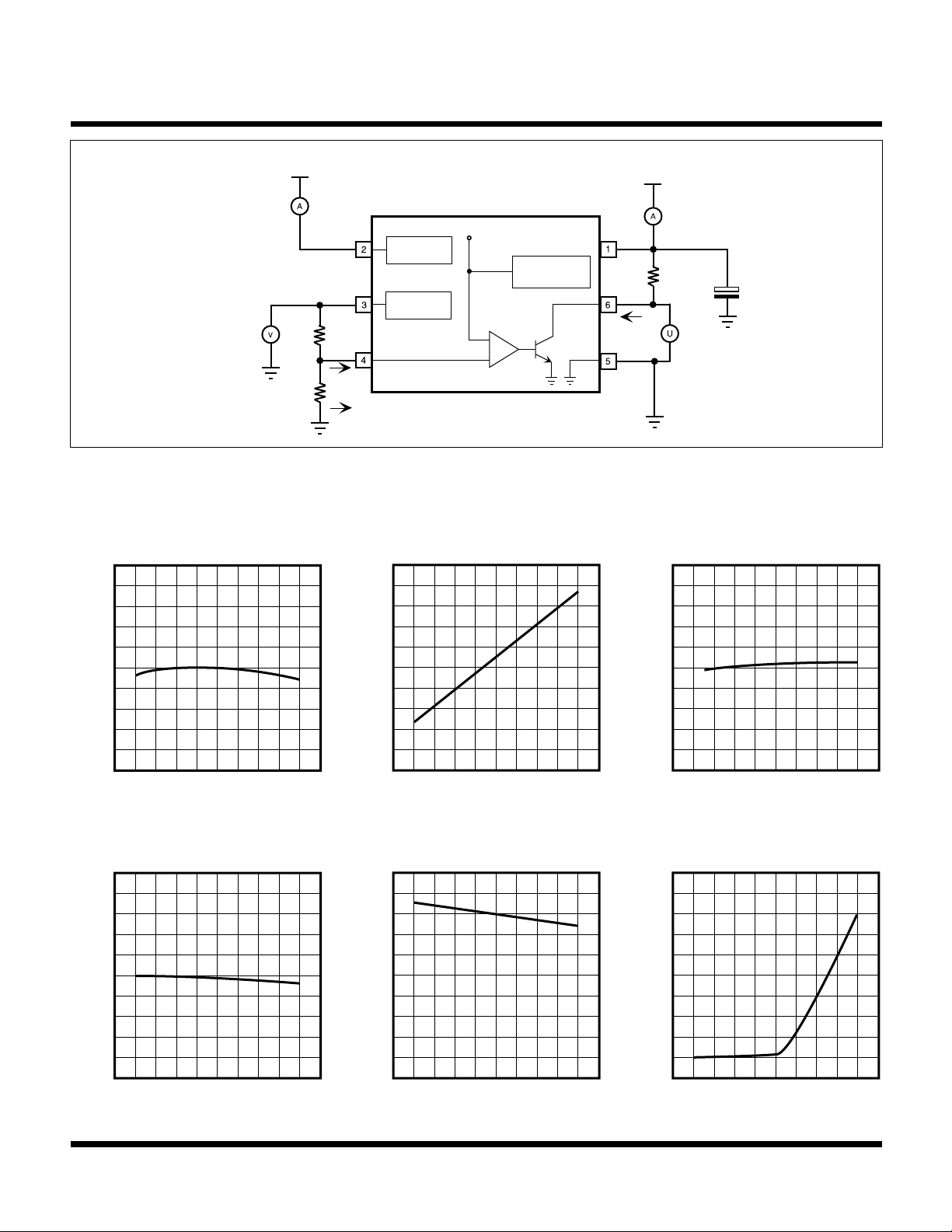
TYPICAL PERFORMANCE CHARACTERISTICS
TA = 25 °C, VCC = 3 V, V
REFERENCE VOLTAGE vs.
TEMPERATURE
R
R
1
2
V
CONT
V
ref
COMP IN
I
IB
I
SH
TEST CIRCUIT
ON/OFF
CIRCUIT
VOLTAGE
REFERENCE
R1 + R2 = 40 kΩ
= 2.4 V, I
CONT
REFERENCE VOLTAGE vs.
OUT
TEMPERATURE
I
R
100 k
CC
3
V
PTAT
TEMPERATURE
SENSOR
+
V
CC
COMP
OUT
GND
I
SINK
= 40 µA, unless otherwise specified.
TK11051
10 µF
LINE REGULATION
1.62
1.61
1.60
ref
1.59
1.58
-40 0 40 80 120
TA (°C)
LOAD REGULATION
1.62
1.61
1.60
ref
1.59
1.6
1.4
1.2
PTAT
1.0
0.8
µ
CONT
-40 0 40 80 120
TA (°C)
CONTROL CURRENT vs.
TEMPERATURE
4
3
2
1
1.62
1.61
1.60
ref
1.59
1.58
µ
CONT
2 4 6 8 10
VCC (V)
CONTROL CURRENT vs.
CONTROL VOLTAGE
4
3
2
1
1.58
0 0.2 0.4 0.6 0.8
I
ref
(mA)
0
-40 0 40 80 120
TA (°C)
0
0 0.6 1.2 1.8 2.4
V
(V)
CONT
January 1999 TOKO, Inc. Page 3
Page 4
TK11051
V
(V)
V
(V)
RR
(dB)
RR
(dB)
I
(
A)
I
(
A)
I
(
A)
I
(
A)
V
(V)
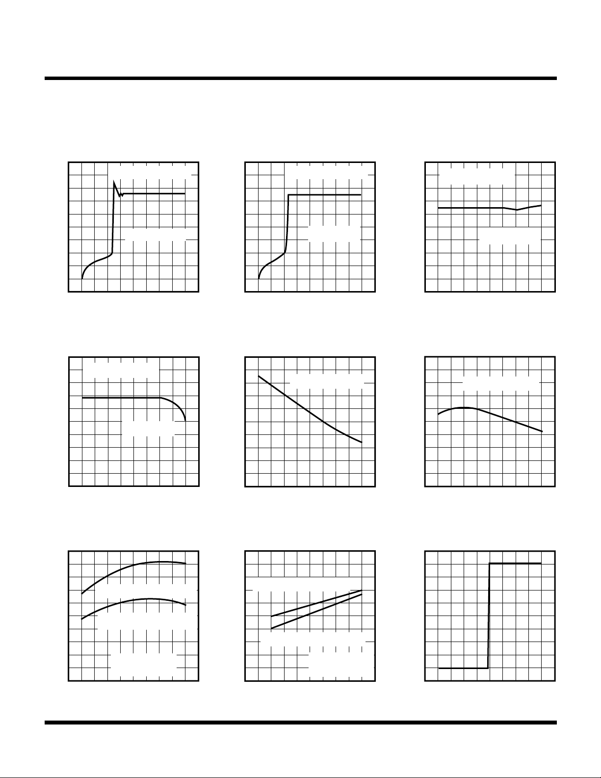
TYPICAL PERFORMANCE CHARACTERISTICS (CONT.)
TA = 25 °C, VCC = 3 V, V
CONT
= 2.4 V, I
= 40 µA, unless otherwise specified.
OUT
CONTROL VOLTAGE RESPONSE A
V
= 0 TO 2.4 V
V
= 100 mVrms
RR
CONT
C
OUT
TIME (ms)
C
OUT
= 0 µF
2.0
1.5
1.0
ref
0.5
0
0 2 4 6 8
RIPPLE REJECTION RATIO B (V
80
60
40
= 0.1 µ F
ref
CONTROL VOLTAGE RESPONSE B
V
= 0 TO 2.4 V
2.0
1.5
1.0
ref
0.5
0
0 2 4 6 8
)
120
100
n
B
INPUT BIAS CURRENT vs.
80
CONT
C
OUT
TIME (ms)
TEMPERATURE
COMP IN > V
= 0 µF
PTAT
RIPPLE REJECTION RATIO A (V
V
= 100 mVrms
RR
C
OUT
f (Hz)
TEMPERATURE
COMP IN < V
µ
80
60
40
20
0
10 100 1 k 10 k 100 k
HYSTERESIS SET CURRENT vs.
1.4
1.3
1.2
SH
= 0.1 µ F
PTAT
ref
)
µ
CC
20
0
10 100 1 k 10 k 100 k
f (Hz)
SUPPLY CURRENT vs.
TEMPERATURE
260
240
220
200
180
COMP OUT = LOW LEVEL
COMP OUT = HIGH LEVEL
R1 + R2 = 40 kΩ
R3 = 100 kΩ
-40 0 40 80 120
TA (°C)
60
40
-40 0 40 80 120
TA (°C)
SUPPLY CURRENT vs.
SUPPLY VOLTAGE
350
COMP OUT = LOW LEVEL
300
µ
250
CC
200
150
COMP OUT = HIGH LEVEL
2 3 4 5 6
V
CC
R1 + R2 = 40 kΩ
R3 = 100 kΩ
(V)
1.1
1.0
-40 0 40 80 120
TA (°C)
REFERENCE VOLTAGE vs.
CONTROL VOLTAGE
1.6
1.2
0.8
ref
0.4
0
0 0.6 1.2 1.8 2.4
V
CONT
(V)
Page 4 January 1999 TOKO, Inc.
Page 5
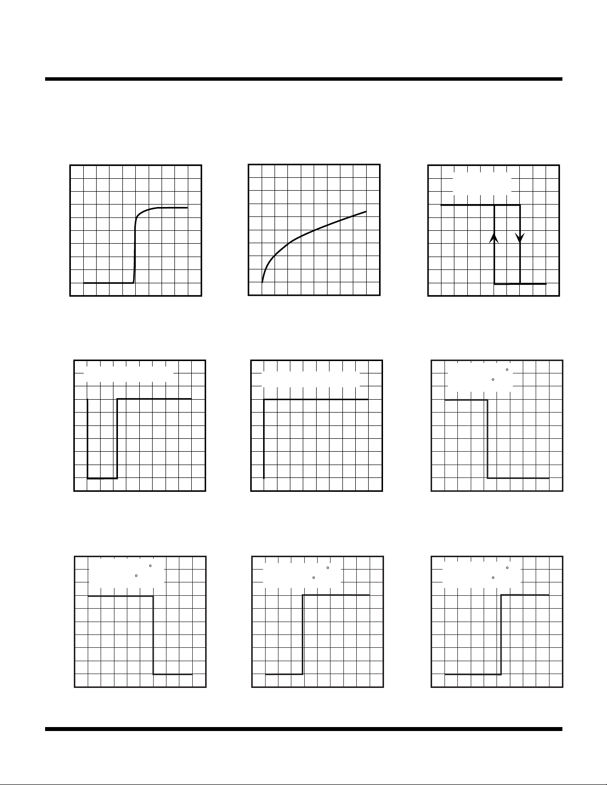
I
(
A)
C
(
V)
COMP
OUT
(V)
TYPICAL PERFORMANCE CHARACTERISTICS (CONT.)
TA = 25 °C, VCC = 3 V, V
CONT
= 2.4 V, I
= 40 µA, unless otherwise specified.
OUT
TK11051
µ
SUPPLY CURRENT vs.
CONTROL VOLTAGE
320
240
160
CC
80
0
0 0.6 1.2 1.8 2.4
V
CONT
CONTROL VOLTAGE RESPONSE
4
V
= 0 TO 2.4 V
CONT
3
2
(V)
COMPARATOR OUTPUT (LOW LEVEL)
vs. OUTPUT SINK CURRENT
160
120
m
80
LL
40
0
0 0.2 0.4 0.6 0.8
I
(mA)
OUT
COMPARATOR INPUT RESPONSE
4
COMP IN = 1.6 TO 0.8 V
3
2
COMPARATOR OUTPUT vs.
TEMPERATURE
T
4
3
2
1
0
65 70 75 80 85
TEMPERATURE RESPONSE A
4
3
2
= 80 °C
SET
TSH = 5 °C
TA (°C)
TA = 25 TO 85 C
T
= 75 C
SET
COMP OUT (V)
1
0
0 2 4 6 8
TIME (ms)
TEMPERATURE RESPONSE B
TA = 25 TO 85 C
4
T
= 80 C
SET
3
2
COMP OUT (V)
1
0
0 5 10 15 20
TIME (s)
COMP OUT (V)
1
0
0 0.2 0.4 0.6 0.8
TIME (ms)
TEMPERATURE RESPONSE C
4
TA = 25 TO -30 C
T
= -20 C
SET
3
2
COMP OUT (V)
1
0
0 5 10 15 20
TIME (s)
COMP OUT (V)
1
0
0 5 10 15 20
TIME (s)
TEMPERATURE RESPONSE D
4
TA = 25 TO -30 C
T
= -25 C
SET
3
2
COMP OUT (V)
1
0
0 5 10 15 20
TIME (s)
January 1999 TOKO, Inc. Page 5
Page 6
TK11051
APPLICATION HINTS
EXTERNAL RESISTORS R1 AND R
The temperature set point (T
SET
2
) and hysteresis (TSH) of
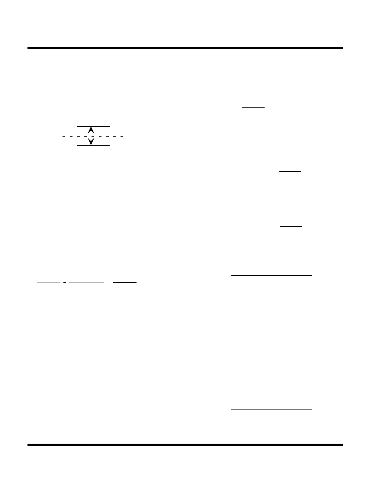
the TK11051 are easily set by two external resistors R1 and
R2. See Figure 1 for clarification of T
T
SH
and TSH.
SET
T
SET
FIGURE 1
The set voltage (V
temperature (T
V
SET
SET
) of the comparator at the set
SET
) is calculated as follows:
= T
SET
x T
C
(1)
where T
That is, T
is an absolute temperature (°K).
SET
(°K) = °C + 273
SET
and TC = 4 mV/°C.
1. For Set Temperatures ≥ 25 °C
V
R2 x V
= =
SET
R1 + R
ref
2
R1 x R2 x I
R1 + R
IB
2
R
2
R1 + R
(V
x
2
ref
(2)
DRRDRDROP
- R1 x IIB)
The hysteresis voltage (VSH) of the comparator can be
calculated as follows:
R1 x R
2
(I
VSH =
(
R1 + R
)
2
- IIB)
X
SH
(5)
where ISH = 1.25 µA
The hysteresis represented as temperature is:
(I
TSH =
R1 x R
(
R1 + R
2
x
)
2
SH
T
- IIB)
C
(6)
Solving for temperature coefficient (TC):
(I
TC =
(
R1 x R
R1 + R
2
)
2
- IIB)
SH
x
T
SH
(7)
Solving for R1 from Equations 3 and 7:
V
x T
ref
R1 =
T
x I
SET
SH
- ( T
SH
- TSH) x I
SET
IB
(8)
where V
= 1.6 V
ref
I
= 0.1 µA
IB
R2 can now be calculated by substituting R1 into Equation 4:
Example:
The temperature coefficient (TC) is calculated by Equations
1 and 2, resulting in:
R1 and R2 when set temperature is 80 °C (T
= 353 °K)
SET
and temperature hysteresis (TSH) is 5 °C.
R
TC =
2
R1 + R
(3)
From Equation 3, R2 is calculated as follows:
T
R2 =
V
- R1 x I
ref
(4)
2
SET
V
- R1 x I
ref
x
x TC x R
- T
IB
SET
T
SET
1
x T
IB
R1 =
1.6 x 5
353 x1.25 µ - ( 353 - 5) x 0.1 µ
R1 = 19.68 k = 20 kΩ
R2 =
353 x 4 m x 19.68 k
1.6 -19.68 k x 0.1 µ - 353 x 4 m
C
R2 = 149.39 k = 150 kΩ
Page 6 January 1999 TOKO, Inc.
Page 7

2. For Set Temperatures < 25 °C
V
x T
ref
R1 =
(T
SET
+ TSH) x I
SH
SH
(9)
T
x TC x R
V
ref
SET
- R1 x I
SH
- T
R2 =
(10)
Example:
APPLICATION HINTS (CONT.)
- T
x I
SET
IB
1
x T
SET
C
TK11051
R1 and R2 when set temperature is -25 °C (T
= 248 °K)
SET
and temperature hysteresis (TSH) is 5 °C.
R1 =
1.6 x 5
(248 + 5) x 1.25 µ - 248 x 0.1 µ
R1 = 27.45 k = 27 kΩ
R2 =
248 x 4 m x 27.45 k
1.6 - 27.45 k x 1.25 µ - 248 x 4 m
R2 = 47.47 k = 47 kΩ
PACKAGE POWER DISSIPATION (PD)
The power dissipation rating of 200 mW represents the
amount of power the device can dissipate without damage
to the IC. Power dissipation should be kept to a minimum
to reduce temperature errors due to self-heating.
January 1999 TOKO, Inc. Page 7
Page 8
TK11051
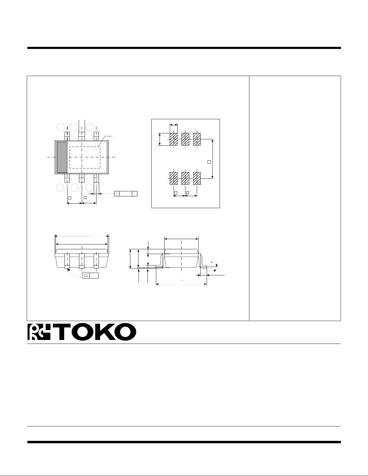
PACKAGE OUTLINE
SOT-23L (SOT-23L-6)
456
123
e e
0.95 0.95
+0.3
- 0.1
3.5
(3.4)
0.1
Dimensions are shown in millimeters
Tolerance: x.x = ± 0.2 mm (unless otherwise specified)
0.32
+0.15
- 0.05
Marking
Marking Information
Marking
TK11051 51C
0.6
1.0
3.0
e1
0.1
M
Recommended Mount Pad
0.3
1.2
1.4 max
+0.15
- 0.05
0 - 0.1
0.15
ee
0.95 0.95
2.2
+ 0.3
3.3
15 max
0.4
Toko America, Inc. Headquarters
1250 Feehanville Drive, Mount Prospect, Illinois 60056
Tel: (847) 297-0070 Fax: (847) 699-7864
TOKO AMERICA REGIONAL OFFICES
Midwest Regional Office
Toko America, Inc.
1250 Feehanville Drive
Mount Prospect, IL 60056
Tel: (847) 297-0070
Fax: (847) 699-7864
Western Regional Office
Toko America, Inc.
2480 North First Street , Suite 260
San Jose, CA 95131
Tel: (408) 432-8281
Fax: (408) 943-9790
Eastern Regional Office
Toko America, Inc.
107 Mill Plain Road
Danbury, CT 06811
Tel: (203) 748-6871
Fax: (203) 797-1223
Semiconductor Technical Support
Toko Design Center
4755 Forge Road
Colorado Springs, CO 80907
Tel: (719) 528-2200
Fax: (719) 528-2375
Visit our Internet site at http://www.tokoam.com
The information furnished by TOKO, Inc. is believed to be accurate and reliable. However, TOKO reserves the right to make changes or improvements in the design, specification or manufacture of its
products without further notice. TOKO does not assume any liability arising from the application or use of any product or circuit described herein, nor for any infringements of patents or other rights of
third parties which may result from the use of its products. No license is granted by implication or otherwise under any patent or patent rights of TOKO, Inc.
Page 8 January 1999 TOKO, Inc.
All Rights Reserved
IC-xxx-TK11051
0798O0.0K
Printed in the USA© 1999 Toko, Inc.
 Loading...