

Page 1
TK10651
8
7
6
5
4
3
2
1
9
FILTER OUT
FILTER IN
COMP OUT
DATA IN
C-DFC
COMP RECT
COMP REF
COMP IN
COMP NF
GND
EXP IN
EXP NF
DATA OUT
EXP RECT
EXP OUT
V
CC
THROUGH
EXP MUTE
EXP REF
COMP MUTE
10 11
12
13
14
15
16
17
18
19
20
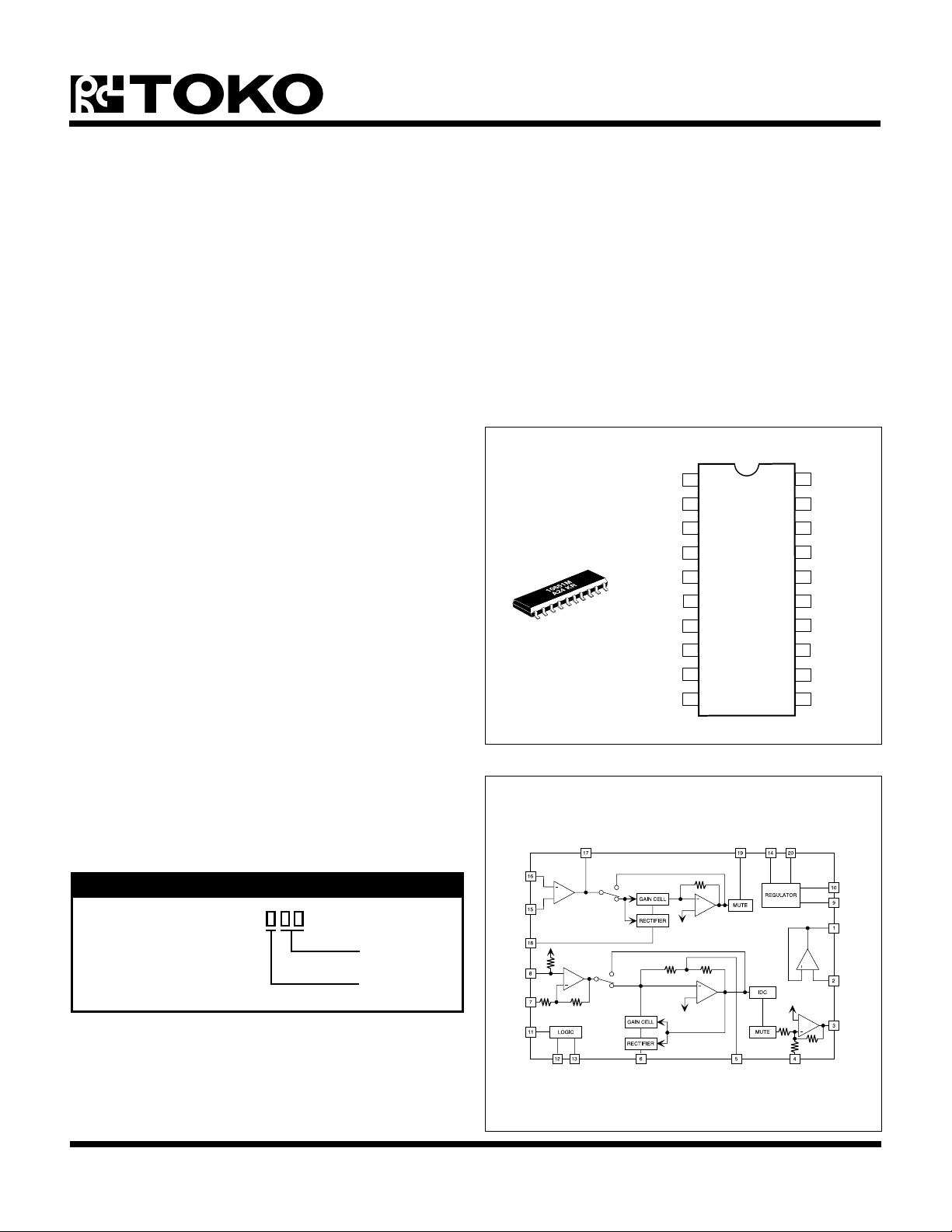
LOW VOLTAGE COMPANDOR
FEATURES
■ Data and Voice Inputs
■ Data and Voice Outputs
■ Low Supply Current
■ Regulated Output
■ Wide Operating Voltage Range
■ Low Standby Current
■ Microphone Amplifier
■ IDC Circuit (Instantaneous Deviation Control)
DESCRIPTION
TK10651 is a noise reduction IC developed mainly for
cordless phones. It is also used for voice and data
communications. It has a built-in compressor circuit to
increase the average modulation level and an expander
circuit to reduce the noise level. The expander restores the
original dynamics of the input signal. The result is a high
quality signal transmission with low noise. Among the
many functions included, analog switching of the input and
output signal is particularly useful in cordless telephones.
Separate data input and output are provided. The audio
signal path can be muted during data transmission. The
signal path used for data transmission bypasses the compressor and expander circuits.
APPLICATIONS
■ Portable Instrumentation
■ Cordless Telephones
■ Handy Talkies
■ Interphones
■ Amateur Radio Transceivers
TK10651
10651M
The TK10651 is available in the SSOP-20 (MFP20)
BLOCK DIAGRAM
surface mount package.
100 kΩ
100 kΩ
VCCEXP REF
GND
COMP REF
FILTER OUT
BUF
AMP
+
FILTER IN
TO V
ref
+
COMP OUT
100 kΩ
DATA IN
DATA OUT
THROUGH
SW
EXPANDER
COMP RECT
30 kΩ
TO V
ref
30 kΩ 30 kΩ
TO V
ref
INPUT AMP
ORDERING INFORMATION
EXP NF
EXP IN
+
THROUGH
SW
TK10651
Tape/Reel Code
PACKAGE CODE
M: Surface Mount
January 2000 TOKO, Inc. Page 1
Package Code
TAPE/REEL CODE
TL: Tape Left
EXP RECT
COMP IN
COMP NF
COMP MUTE
TO V
ref
100 kΩ
+
3.3 kΩ 51 kΩ
THROUGH
MIC AMP
EXP MUTE
EXP OUT
+
SUM
AMP
SUM
AMP
+
C-DCFB
Page 2
TK10651
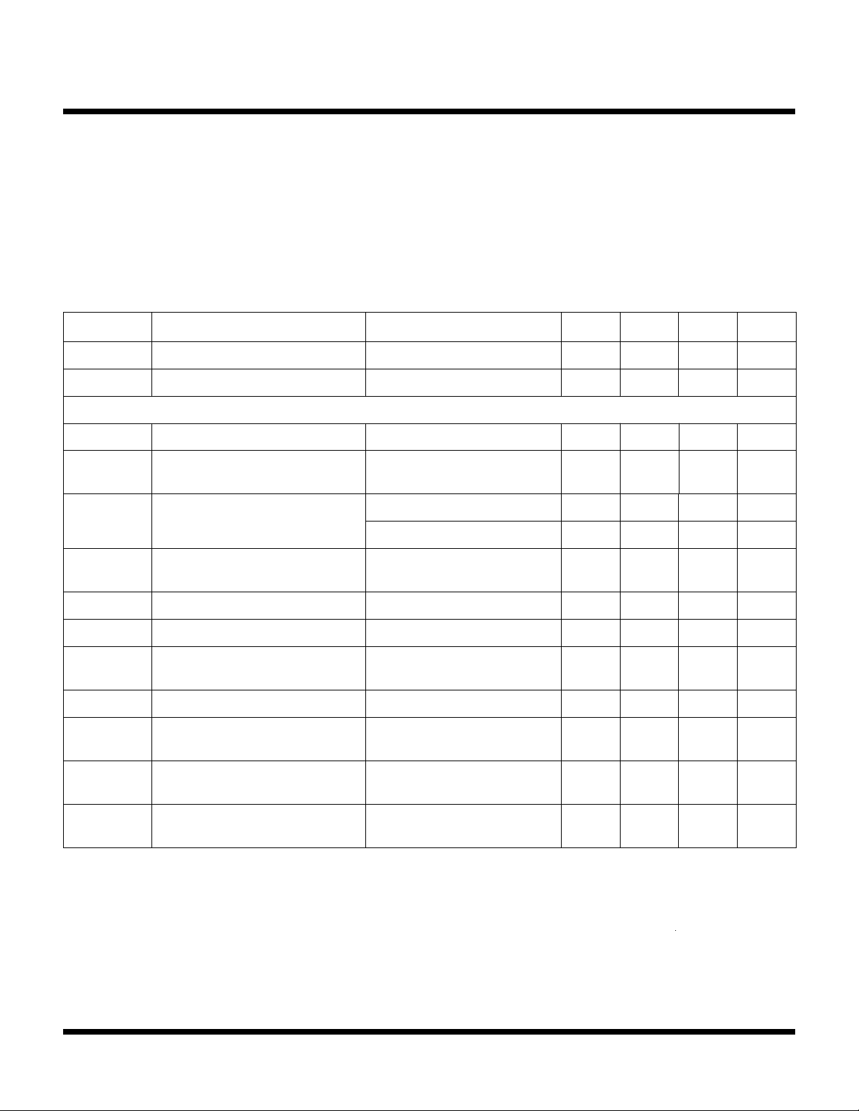
ABSOLUTE MAXIMUM RATINGS
Supply Voltage .........................................................10 V
Power Dissipation (Note 1) ................................410 mW
Junction Temperature .......................................... 150 °C
Operating Voltage Range..............................2.4 to 7.0 V
TK10651 ELECTRICAL CHARACTERISTICS
Test conditions: V
LOBMYSRETEMARAPSNOITIDNOCTSETNIMPYTXAMSTINU
= 3.0 V, f = 1.0 kHz, RL = 10 kΩ, TA = 25 °C, unless otherwise specified.
CC
Input Frequency ................................................. 100 kHz
Storage Temperature Range ...................-55 to +150 °C
Operating Temperature Range ..................-20 to +70 °C
Lead Soldering Temp. (10 sec.).......................... 235 °C
I
V
Z
V
∆G
∆G
V
V
CC
HT
tnerruCylppuSlangisoN00.405.6Am
egatloVdlohserhT31,21,11sniP51.103.154.1V
rosserpmoC
CNI
CNI
C
CT
DHT
C
CON
TTA
C
CMIL
DVG
lanimreT
ecnadepmItupnI09021kΩ
V
egatloVtupnIdradnatS
rorrEniaG
ecnereffiDffO/nOhguorhT
noitrotsiDcinomraHlatoTV
CO
V
NI
V
NI
V
NI
V
NI
NI
Vm003=
smr
)2etoN(,Bd0=
85.2171Vm
)2etoN(,Bd02-=5.0-05.0+Bd
)2etoN(,Bd04-=0.1-00.1+Bd
,dednuorg21niP,Bd0=
)2etoN(
5.1-05.1+Bd
Bd0=5.00.1%
egatloVesioNtuptuO026=gR Ω )2etoN(,0.35.5Vm
V
noitaunettAetuM
NI
)2etoN(
,dednuorg11niP,Bd0=
0608Bd
egatloVgnitimiL51.153.105.1V
ATADrofniaGegatloV
Vm003=egatlov4niP
smr
5.0-05.0+Bd
smr
smr
P-P
V
Note 1: Power dissipation is 410 mW in free air. Derate at 3.3 mW/°C for operation above 25 °C.
Note 2: Evaluated by CCITT standard P.53 noise filter.
D)XAM(TUO
TC
C
lanimreTATAD
klaTssorC
rofegatloVtuptuOmumixaM
VpxE
NI
026=gR Ω )2etoN(,
tnioP%01=DHT008009Vm
Vm03=
,
smr
53-03-Bd
smr
Page 2 January 2000 TOKO, Inc.
Page 3
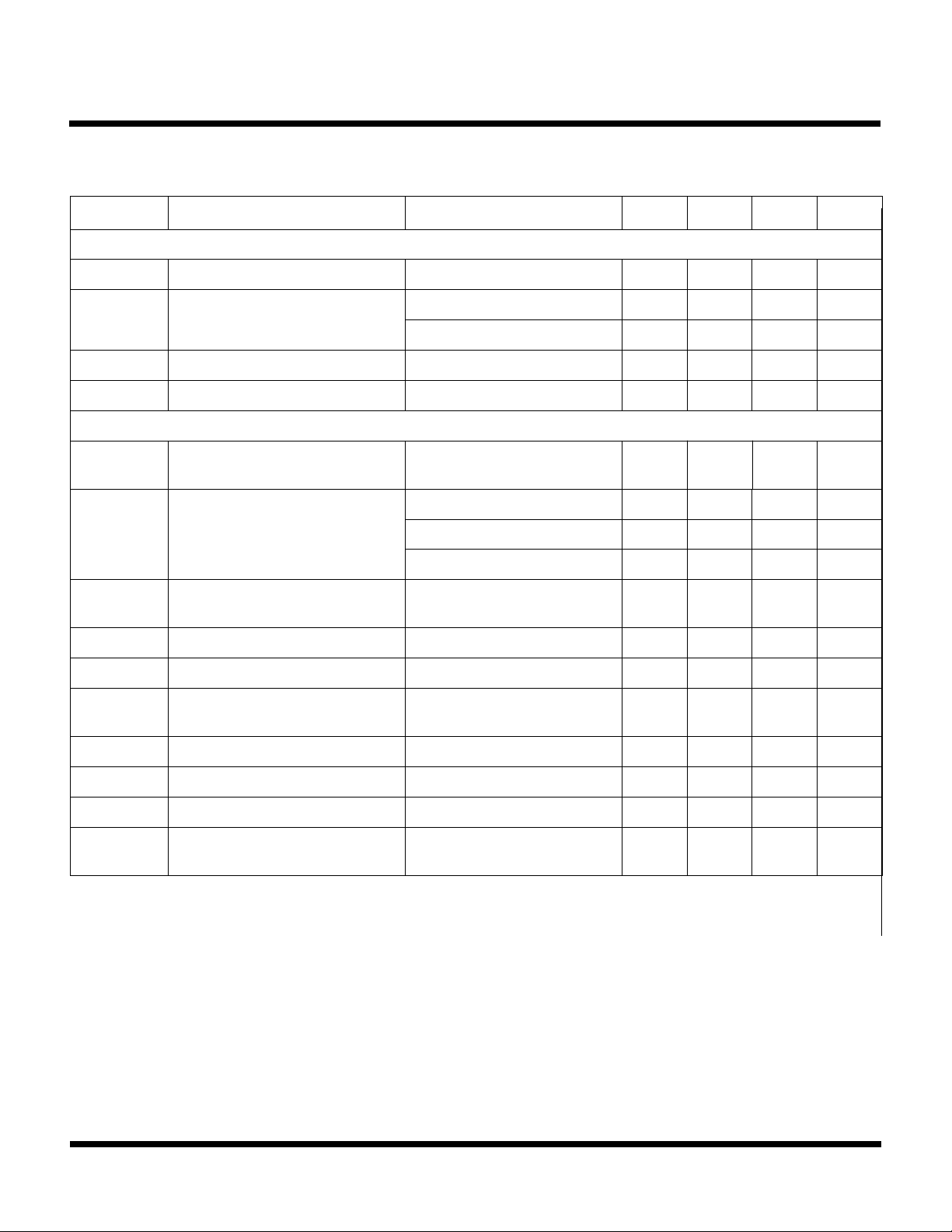
TK10651 ELECTRICAL CHARACTERISTICS (CONT.)
Test conditions: V
LOBMYSRETEMARAPSNOITIDNOCTSETNIMPYTXAMSTINU
= 3.0 V, f = 1.0 kHz, RL = 10 kΩ, TA = 25 °C, unless otherwise specified.
CC
reifilpmAreffuB
TK10651
BVGniaGegatloVV
∆f
V
DHT
B
B)XAM(TUO
scitsiretcarahCycneuqerF
noitrotsiDcinomraHlatoTV
egatloVtuptuOmumixaMtnioP%01=DHT055007Vm
NI
V
NI
V
NI
NI
Vm003=
smr
Vm003=
smr
Vm003=
smr
zHk3=f,3-Bd
zHk03=f,06-Bd
smrVm003=20.01.0%
rednapxE
V
∆G
∆G
V
V
ETUO
E
ET
DHT
E
EON
TTA
E
rorrEniaG
noitaunettA
egatloVtuptuOdradnatS
ecnereffiDffO/nOhguorhT
noitrotsiDcinomraHlatoTV
egatloVesioNtuptuO026=gR Ω )2etoN(,0103Vµ
NI
)2etoN(
V
NI
V
NI
V
NI
V
NI
)2etoN(
NI
V
NI
Bd0=5.05.1%
)2etoN(
,Bd0=smrVm03=
)2etoN(,Bd01-=5.0-05.0+Bd
)2etoN(,Bd02-=0.1-00.1+Bd
)2etoN(,Bd03-=5.1-00.2+Bd
5.0-05.0+Bd
smr
011031061Vm
,dednuorg21niP,Bd0=
,dednuorg31niP,Bd0=
5.2-0.1-5.0+Bd
0608Bd
smr
smr
V
E)XAM(TUO
IVG.pmAtupnIrofniaGegatloVV
V
Note 2: Evaluated by CCITT standard P.53 noise filter.
I)XAM(TUO
TC
E
klaTssorC
egatloVtuptuOmumixaMtnioP%01=DHT007008Vm
NI
Bd0=5.415.515.61Bd
egatloVtuptuOmumixaMtnioP%01=DHT054005Vm
VpmoC
V=
NI
026=gR Ω )2etoN(,
,
CNI
07-06-Bd
January 2000 TOKO, Inc. Page 3
smr
smr
Page 4
TK10651
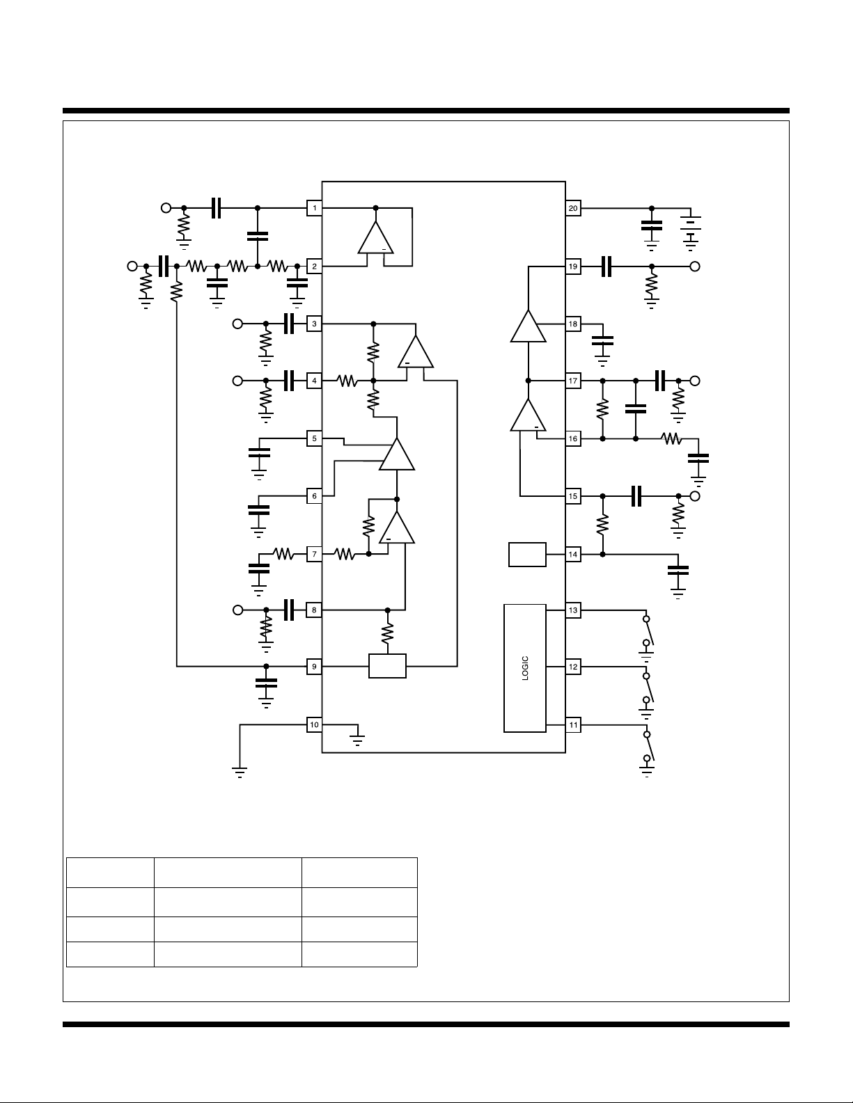
TEST CIRCUIT
FILTER
IN
620 Ω
FILTER
OUT
1.0 µF
1.0 µF
10 kΩ
100
kΩ
COMPRESS
OUT
DATA
COMPRESS
IN
10 kΩ10 kΩ
6800 pF
IN
0.47 µF
10 kΩ
620 Ω
620 Ω
18000 pF
10 kΩ
1000 pF
1.0 µF
0.1 µF
22 µF
2.2 µF
9.1 kΩ
0.047 µF
100 kΩ
100 kΩ
51 kΩ
3.3 kΩ
V
CC
10 µF
+
100 kΩ
COMP
+
100 kΩ
1.0 µF
EXP
+
51 kΩ
+
100 kΩ
REG
2.2 µF
10 kΩ
2.2 µF
50 pF
10 kΩ
0.047 µF
620
MUTE
EXPAND
10 kΩ
4.7 µF
V
CC
EXPAND
OUT
DATA
OUT
1.0 µF
EXPAND
IN
REG
4.7 µF
SWITCH PIN HIGH (OPEN OR VCC) LOW (GND)
Switch pins priority order:
THROUGH
MUTE
COMPRESS
High > pins 11 and 13 > pin 12 > low.
Pin 11 Comp Mute OFF Comp Mute ON
Pin 12 Compandor Through
Pin 13 Exp Mute OFF Exp Mute ON
Page 4 January 2000 TOKO, Inc.
Page 5
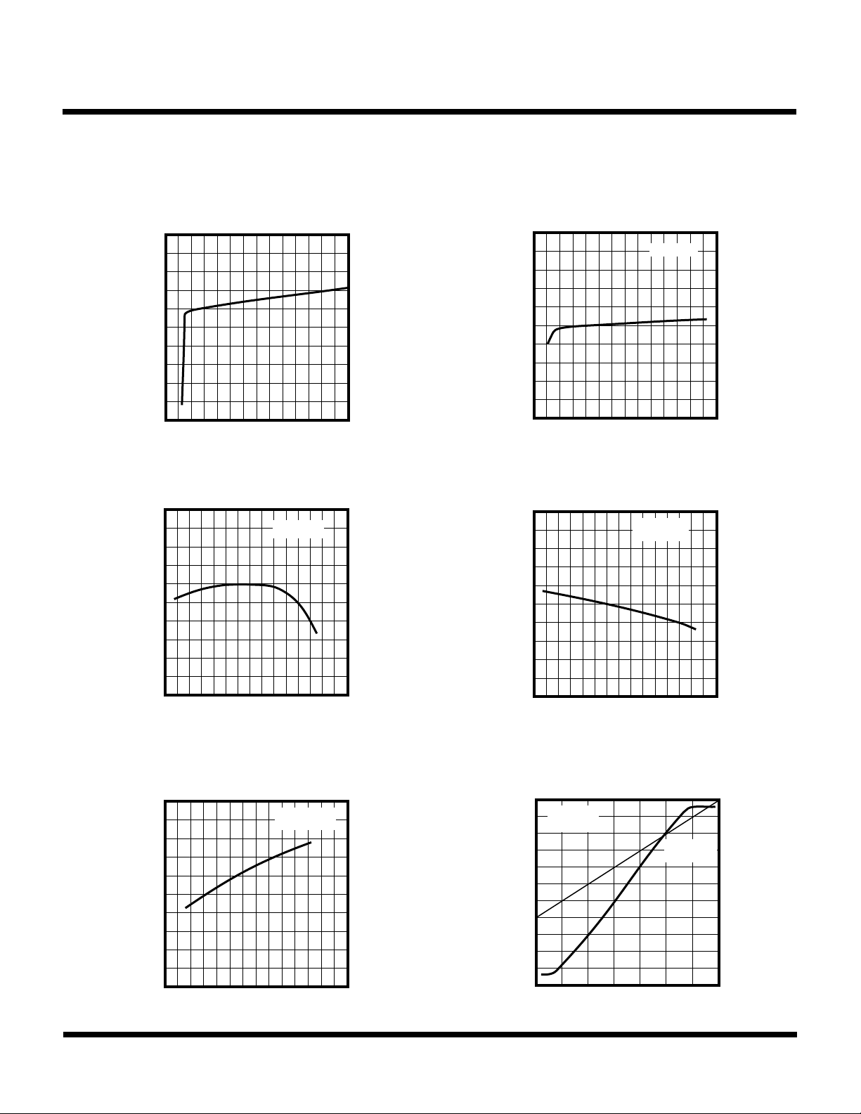
DC CHARACTERISTICS
1.5
1.48
1.46
(V)
ref
V
1.44
1.42
1.4
234 678
TYPICAL PERFORMANCE CHARACTERISTICS
REFERENCE VOLTAGE vs.
SUPPLY VOLTAGE
5
VCC (V)
SUPPLY CURRENT vs. SUPPLY
6
5
(mA)
4
CC
I
3
2
234 678
TK10651
VOLTAGE
NO SIGNAL
5
VCC (V)
REFERENCE VOLTAGE vs.
AMBIENT TEMPERATURE
1.5
1.48
1.46
(V)
ref
V
1.44
1.42
1.4
-40 -20 0 40 60 80
20
TA (°C )
EXPANDER AC CHARACTERISTICS
OUTPUT REFERENCE VOLTAGE
vs. SUPPLY VOLTAGE
2
1
(dB)
0
OE
V
-1
-2
234 678
VCC (V)
5
VCC = 3.0 V
fIN = 1.0 kHz
100
100 mV(rms)
SUPPLY CURRENT vs. AMBIENT
TEMPERATURE
6
5
(mA)
4
CC
I
3
2
-40 -20 0 40 60 80
20
TA (°C )
OUTPUT VOLTAGE vs.
INPUT VOLTAGE
0
VCC = 3.0 V
-10
fIN = 1.0 kHz
-20
-30
-40
(dB)
-50
OUT
-60
V
-70
-80
-90
-100
-110
-70 -60 -50 -40 -30 -20 -10
-80
30 mV(rms)
VIN (dB)
VCC = 3.0 V
NO SIGNAL
REFERENCE
100
LEVEL
January 2000 TOKO, Inc. Page 5
Page 6
TK10651
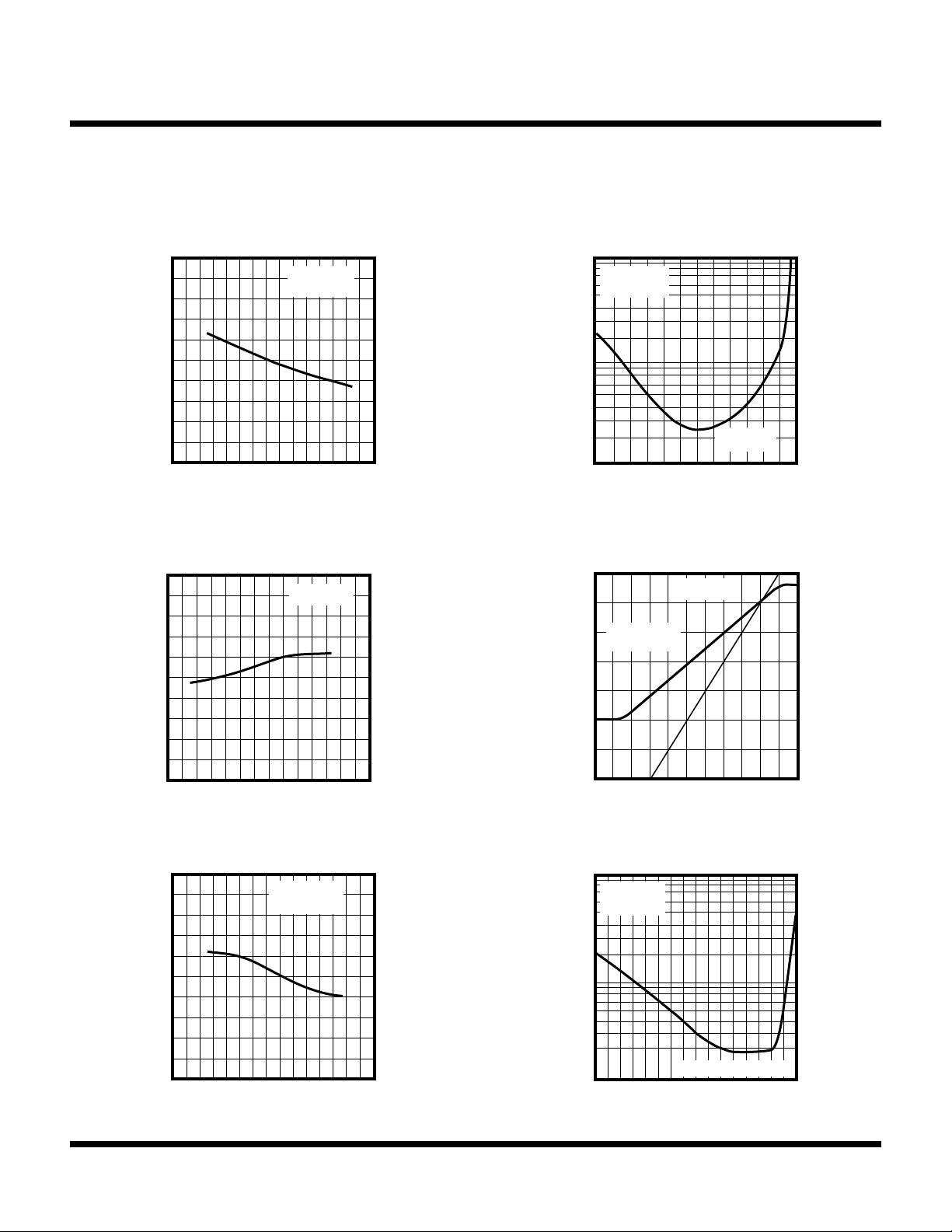
TYPICAL PERFORMANCE CHARACTERISTICS (CONT.)
EXPANDER AC CHARACTERISTICS (CONT.)
OUTPUT REFERENCE VOLTAGE
vs. AMBIENT TEMPERATURE
2
1
(dB)
0
OE
V
-1
-2
-40 -20 0 40 60 80
20
TA (°C )
COMPRESSOR AC CHARACTERISTICS
INPUT REFERENCE VOLTAGE
vs. SUPPLY VOLTAGE
2
1
(dB)
0
IN C
V
-1
VCC = 3.0 V
fIN = 1.0 kHz
fIN = 1.0 kHz
100
300 mv(rms)
(dB)
V
DISTORTION vs.
INPUT VOLTAGE
10
VCC = 3.0 V
fIN = 1.0 kHz
5
2
1
THD (%)
0.5
0.2
0.1
-50 -45 -40 -35
OUTPUT VOLTAGE vs.
INPUT VOLTAGE
0
-10
VCC = 3.0 V
-20
fIN = 1.0 kHz
-30
OUT
-40
-50
REFERENCE
VIN (dB)
REFERENCE
LEVEL
LEVEL
-30 -25 -20
-2
234 678
5
VCC (V)
INPUT REFERENCE VOLTAGE
vs. AMBIENT TEMPERATURE
2
VCC = 3.0 V
fIN = 1.0 kHz
-60
-70
10
-120
VCC = 3.0 V
fIN = 1.0 kHz
5
-100 -80 -60 -40 -20
V
IN
(dB)
10 mV(rms)
DISTORTION vs.
INPUT VOLTAGE
1
(dB)
IN C
V
-1
0
2
THD (%)
1
.5
.2
-2
-40 -20 0 40 60 80
20
TA (°C )
100
.1
-70 -65 -55 -50
-60 -40
REFERENCE LEVEL
-45 -35 -30
VIN (dB)
Page 6 January 2000 TOKO, Inc.
Page 7
TYPICAL PERFORMANCE CHARACTERISTICS (CONT.)
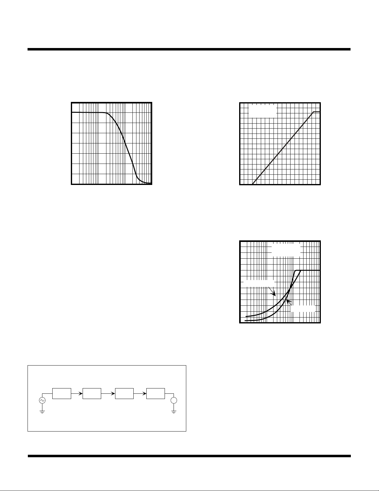
THIRD ORDER LPF CHARACTERISTICS
TK10651
OUTPUT VOLTAGE vs. THIRD
ORDER LPF INPUT FREQUENCY
10
0
-10
-20
(dB)
-30
OUT
V
-40
-50
-60
-70
0.1 0.2 0.5 1
2 5 10 20 50
f
(kHz)
IN
100
USING THE COMPANDOR TO IMPROVE S/N
This section provides an example of using the compandor
to improve S/N in a narrow band FM communication
system. In the test configuration below, the compressor
modulation level was measured as a function of the input
voltage to demonstrate the improvement resulting from the
use of the compressor. An audio signal is connected into
the compressor and the output is measured with the
modulation meter connected to the external modulation
input of the FM signal generator. The compressor's reference input level was set to produce ±3.0 kHz frequency
deviation. As shown in the graph on the right, the peak
deviation remains the same when the compressor is used,
but a wider input range is obtained. The built-in characteristics of the IDC circuit limit the maximum frequency deviation to ±4.5 kHz.
0
-10
-20
(dBV)
-30
OUT
-40
V
-50
-60
-70
-90
7
6
5
4
m (± kHz )
3
2
1
0
0.1 0.2 0.5 1
OUTPUT VOLTAGE VS. THIRD
ORDER LPF INPUT VOLTAGE
VCC = 3.0 V
f
= 1.0 kHz
IN
-80 -70 -60 -50 -40 -30 -20 -10 0
MODULATION LEVEL vs.
COMPRESSOR
VIN (dBV)
COMPRESSOR INPUT
VCC = 3.0 V
f
= 1.0 kHz
MOD
THROUGH
2 5 1020 50
VIN (mVrms)
100
TEST CONFIGURATION
TK10651
COMP
FM
SG
FM IF IC
TK10487
TK10651
EXP
V
January 2000 TOKO, Inc. Page 7
Page 8
TK10651
TYPICAL PERFORMANCE CHARACTERISTICS (CONT.)
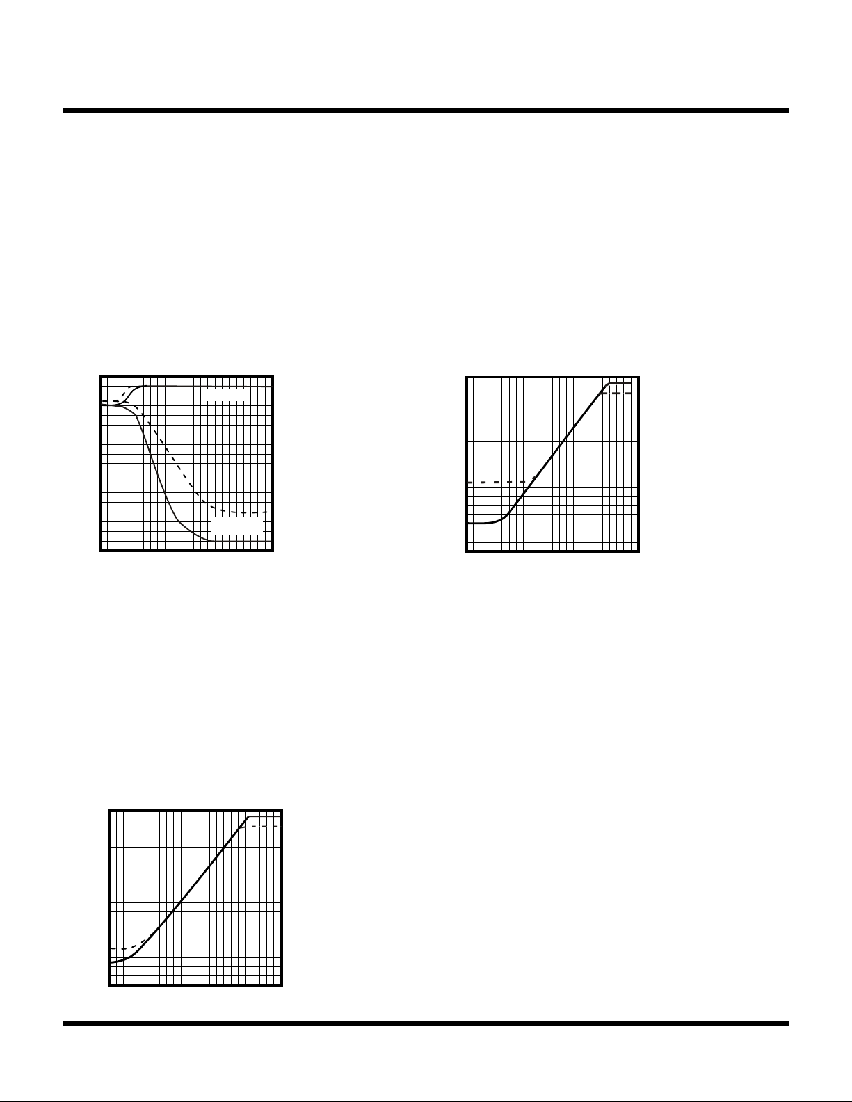
USING THE COMPANDOR TO IMPROVE S/N (CONT.)
The improvement resulting from the expander is expressed
by measuring the overall characteristics of the FM IF
System (TK10487M). The signal generator was switched
to internal modulation and the output is defined as 0 dB
when the RF input = 80 dBµ. As the graph below indicates,
the noise is reduced when the expander is used, and good
S/N ratio is maintained even when the RF signal input is
weak.
OUTPUT VOLTAGE RATIO vs.
COMPANDOR RF INPUT
(dB)
OUT
V
-10
-20
-30
-40
-50
-60
-70
-80
0
-20
0 20406080100
VIN (dBu)
SIGNAL
NOISE
VCC = 3.0 V
f
= 10.245 MHz
OSC
DEV = ± 3.0 kHz
f
= 1.0 kHz
MOD
FILTER : CCITT P.53
IF IC : TK10487M
NO PRE-EMPHASIS
OR DE-EMPHASIS
SOLID LINE:
COMPRESSOR
DASHED LINE: THROUGH
The following graph shows the characteristics when the RF
input is weak (RF IN = 30 dBµ). There is a great difference
when the compandor is used with a weak RF input. When
the through function is used (noise reduction off), the output
is lost in noise as the compressor input drops below –80
dBV; but when the compandor function is used, it remains
level below –100 dBV. With a weak RF input, dynamic
range is extended by 30 dB.
OUTPUT VOLTAGE RATIO
(FOR WEAK RF INPUT SIGNAL)
vs. COMPANDOR INPUT
(dB)
OUT
V
10
-10
-20
-30
-40
-50
-60
-70
-80
0
-110
-90 -70 -50 -30 -10
VIN (dBV)
VCC = 3.0 V
f
= 10.245 MHz
OSC
f
= 1.0 kHz
MOD
FILTER : CCITT P.53
IF IC :TK10487M
NO PRE-EMPHASIS
OR DE-EMPHASIS
SOLID LINE:
COMPRESSOR
DASHED LINE: THROUGH
Finally, the overall characteristics are measured using both
the compressor and the expander. The output is measured
when the compressor's input is at –40 dBµV and the
frequency deviation is ±3.0 kHz.
The graph below shows the characteristics when the RF
input is strong (RF IN = 80 dBµ). The dynamic range is
increased by more than 12 dB when the compandor is
used.
OUTPUT VOLTAGE RATIO (FOR
STRONG RF INPUT SIGNAL)
vs. COMPANDOR RF INPUT
(dB)
OUT
V
-10
-20
-30
-40
-50
-60
-70
-80
10
0
-120
-90 -70 -50 -30 -10
VIN (dBV)
VCC = 3.0 V
f
= 10.245 MHz
OSC
f
= 1.0 kHz
MOD
FILTER : CCITT P.53
IF IC :TK10487M
NO PRE-EMPHASIS
OR DE-EMPHASIS
SOLID LINE:
COMPRESSOR
DASHED LINE: THROUGH
The effects of the compandor within a narrow band FM
communications system was demonstrated while a coaxial
cable was used in place of transmission through free
space. The signal source was an FM signal generator
although there are some differences when actual transmission is through free space. However, the test configuration
used in this experiment is useful in understanding the
effects of the compandor.
Page 8 January 2000 TOKO, Inc.
Page 9
APPLICATION INFORMATION
TK10651
COMPRESSOR
By placing the data input pin following the compressor
circuit, a data signal can be transmitted without being
compressed. Audio from the microphone can be connected
directly to the IC, because it passes through the built-in
microphone amplifier (the gain is adjustable). Since there is
a built-in limiter to prevent overmodulation, it is not necessary to add an external Instantaneous Deviation Control
(IDC) circuit; furthermore, a Low Pass Filter (LPF) up to the
third order can be constructed using the buffer amplifier.
When a data signal is being transmitted, the unneeded
audio can be cut by engaging the mute switch.
EXPANDER
A wide range of applications are made possible because all
of the input amplifier pins are accessible. A LPF of up to the
third order can be constructed at the input, and with an
external resistor, it can be used as an amplifier. If the data
out pin is used for the output, a data signal can be extracted
without passing through the expander. During data transmission, the audio signal system can be inhibited by using
the mute switch.
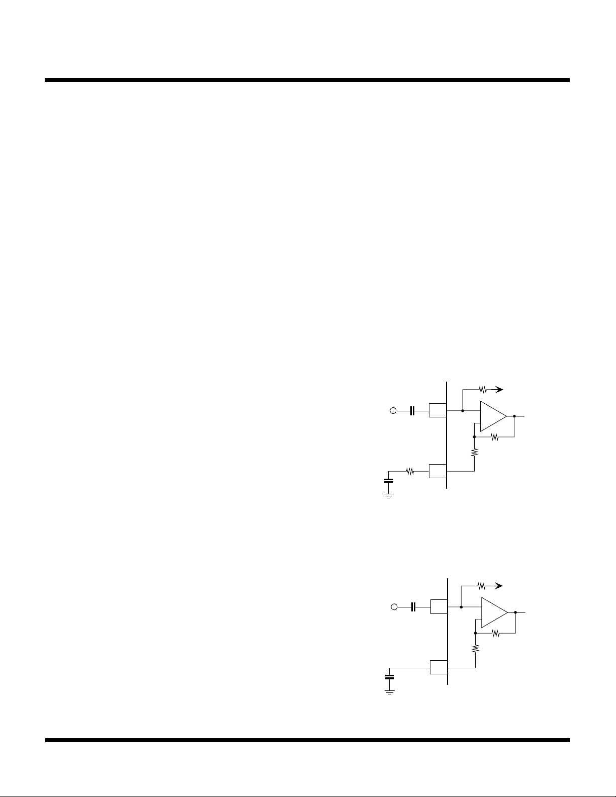
COMPRESSOR MICROPHONE AMPLIFIER
The input pin connects to the reference voltage through a
100 kΩ bias resistor, therefore external bias is not necessary. The microphone amplifier gain can be adjusted by
connecting an external resistor to NF pin 7. The gain is
highest when no resistor is added, and the standard input
level is 3 mV. When an external resistor of 9.1 kΩ is added,
the standard input level is about a 10 mV; when the external
resistor value is 68 kΩ, the standard input level is 30 mV.
The input can accommodate a variety of microphones by
adjusting the gain to match the microphone's output voltage.
The user should set the gain and input level so that the
output level at pin 3 is normally 300 mV (standard level).
~10 mV
100 k
COMP IN
8
V
REF
+
-
~3 mV
COMP NF
9.1 k
COMP IN
COMP NF
100 k
+
-
51 k
51 k
V
REF
3.3 k
7
7
8
3.3 k
7
January 2000 TOKO, Inc. Page 9
Page 10
TK10651
APPLICATION INFORMATION (CONT.)
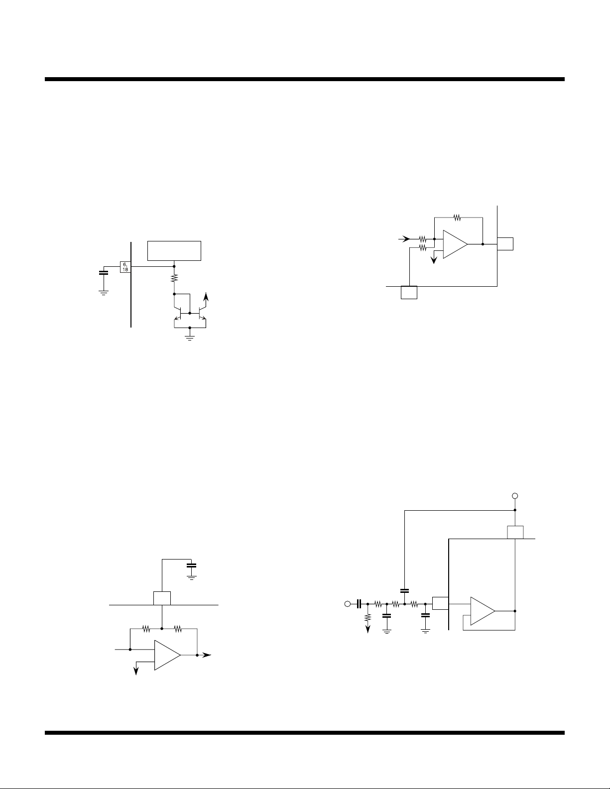
RECTIFIER
The rectifier's smoothing capacitor pins (6 & 18), determine
the smoothing characteristics and the time constants of the
compressor and the expander. The time constant is determined by the external capacitor value and the internal 10
kΩ resistance.
RECTIFIER
10 k
TO GAIN CELL
COMPRESSOR SUMMING AMPLIFIER
The compressor summing amplifier (SUM AMP) must have
unity DC gain and the AC open loop gain is high. Since the
feedback resistors are internal to the device, only one
external capacitor is needed between pin 5 and GND. The
cutoff frequency is determined by the external capacitor
and the internal resistors.
COMPRESSOR DATA INPUT
An inverting amplifier is used at the DATA input. The
internal input resistors are 100 kΩ, and the DC bias (V
REF
is about 1.5 V. The maximum load at the output pin is 10 kΩ.
100 k
COMP OUT
3
FROM COMP
DATA IN
4
100 k
100 k
TO V
+
-
REF
BUFFER AMPLIFIER
Up to a third order LPF (for example, a splatter filter) can be
constructed using this amplifier. The maximum load at the
output pin is 10 kΩ. The non-inverting input of the amplifier
is not biased internally, therefore an external bias is needed
(for example Pin 3 V
) whenever this pin is not direct-
ref
coupled from the compressor output pin (pin 3).
1
)
3 kHz LPF
18000 p
C-DCFB
5
30 k30 k
+
-
100 k
TO V
10 k 10 k 10 k
REF
2
1000 p6800 p
+
-
Page 10 January 2000 TOKO, Inc.
Page 11
APPLICATION INFORMATION (CONT.)
11,12,13
TK10651
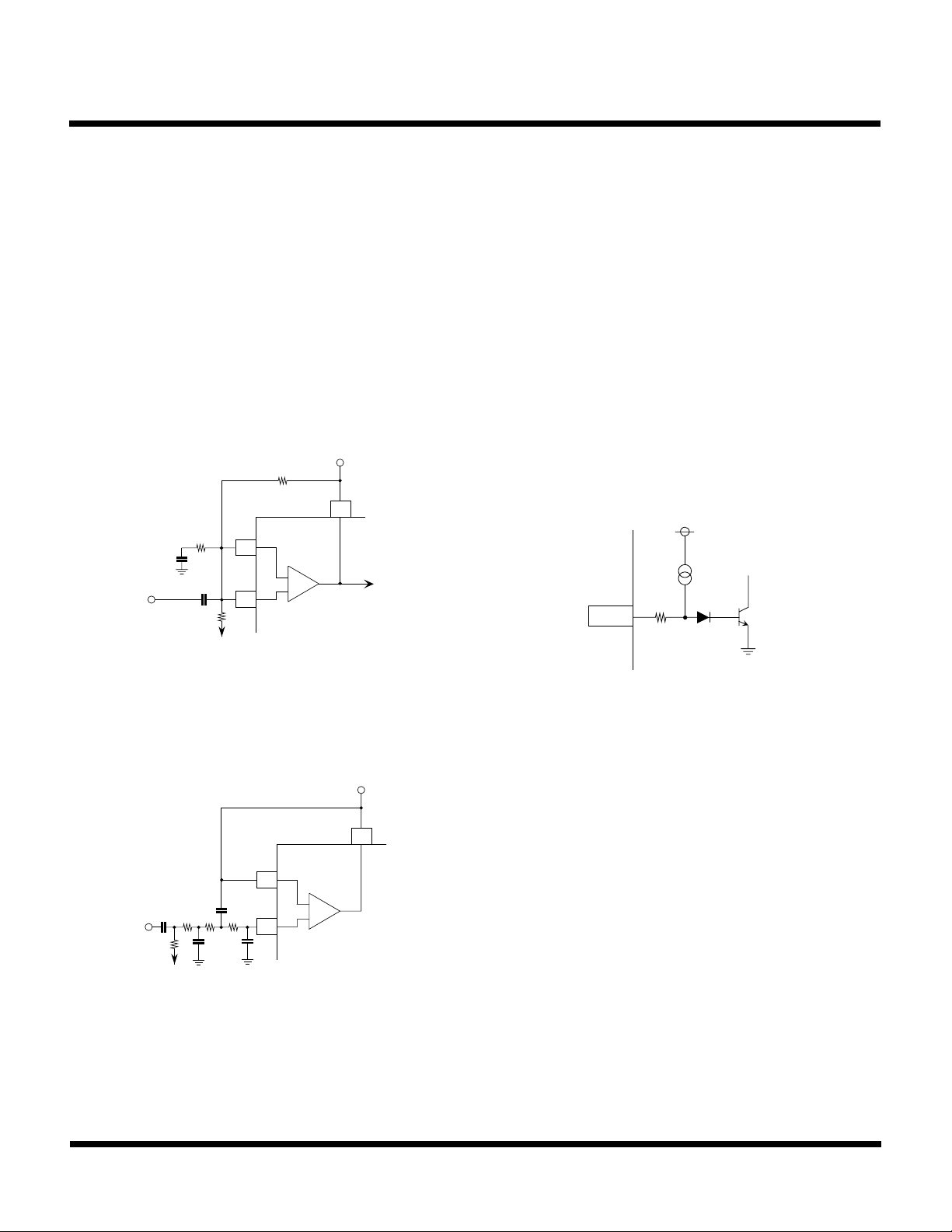
EXPANDER INPUT AMPLIFIER
The non-inverting and inverting input pins as well as the
output pins are available, and can be used as a buffer amp
or filter amp. A data signal can be obtained from the output
pin, without passing through the expander. The input level
and amplifier gain should be set to provide 180 mV(rms)
standard level at the data output pin (pin 17). The expander
input amplifier is not DC biased internally, therefore a bias
voltage from the expander's V
pin (pin 14) should be
REF
used. The maximum allowable load at the output pin is 10
kΩ.
EXP
OUT
51 k
10 k
100 k
TO V
EXP NF
REF
16
EXP
15
DATA OUT
+
IN
-
17
REFERENCE VOLTAGE SOURCE
(PINS 9 AND 14)
Pin 9 is the reference voltage pin for the compressor and
pin 14 is the reference voltage pin for the expander. The
reference voltages are obtained from an internal band gap
reference and used as the bias source for each section.
SWITCH CIRCUIT (PINS 11, 12, and 13)
The compressor's and expander's mute pins and the through
pin (noise reduction is off) are pulled up by internal current
sources, therefore they do not need an external pull up.
Concerning the switching logic, refer to the table in the Test
Circuit section.
AMPLIFIER (GAIN = 6)
EXP NF
EXP
18000 p
10 k 10 k 10 k
100 k
TO V
REF
1000 p6800 p
3 kHz LPF
DATA
17
OUT
16
IN
15
+
-
January 2000 TOKO, Inc. Page 11
Page 12
TK10651
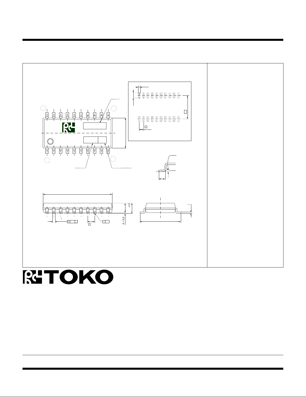
PACKAGE OUTLINE
SSOP-20 (MFP20)
20
1
10.2
0.15
0.05
0.35
M
0.10
AAAAA
YYY
KR
e
1.0
Marking Information
0.5
Mark
11
10
Country of OriginLot No.
0.1
1.2
e
1.0
4.4
1.4
Recommended Mount Pad
1.5
0.5
±0.3
6.0
5.4
e1
0°~10°
0.15
0.05
0.15
Marking
TK10651 10651
Dimensions are shown in millimeters
Tolerance: x.x = ± 0.2 mm (unless otherwise specified)
Toko America, Inc. Headquarters
1250 Feehanville Drive, Mount Prospect, Illinois 60056
Tel: (847) 297-0070 Fax: (847) 699-7864
TOKO AMERICA REGIONAL OFFICES
Midwest Regional Office
Toko America, Inc.
1250 Feehanville Drive
Mount Prospect, IL 60056
Tel: (847) 297-0070
Fax: (847) 699-7864
Western Regional Office
Toko America, Inc.
2480 North First Street , Suite 260
San Jose, CA 95131
Tel: (408) 432-8281
Fax: (408) 943-9790
Eastern Regional Office
Toko America, Inc.
107 Mill Plain Road
Danbury, CT 06811
Tel: (203) 748-6871
Fax: (203) 797-1223
Semiconductor Technical Support
Toko Design Center
4755 Forge Road
Colorado Springs, CO 80907
Tel: (719) 528-2200
Fax: (719) 528-2375
Visit our Internet site at http://www.tokoam.com
The information furnished by TOKO, Inc. is believed to be accurate and reliable. However, TOKO reserves the right to make changes or improvements in the design, specification or manufacture of its
products without further notice. TOKO does not assume any liability arising from the application or use of any product or circuit described herein, nor for any infringements of patents or other rights of
third parties which may result from the use of its products. No license is granted by implication or otherwise under any patent or patent rights of TOKO, Inc.
Page 12 January 2000 TOKO, Inc.
All Rights Reserved
IC-231-TK11031
0798O0.0K
Printed in the USA© 1999 Toko, Inc.
 Loading...