

Datasheet TISP3180F3SL, TISP3180F3DR, TISP3180F3P, TISP3180F3D, TISP3150F3SL Datasheet (Power Innovations)
...Page 1
TISP3125F3, TISP3150F3, TISP3180F3
DUAL SYMMETRICAL TRANSIENT
VOLTAGE SUPPRESSORS
PRODUCT INFORMATION
1
MARCH 1994 - REVISED SEPTEMBER 1997Copyright © 1997, Power Innovations Limited, UK
Information is current as of publication date. Products conform to specifications in accordance
with the terms of Power Innovations standard warranty. Production processing does not
necessarily include testing of all parameters.
TELECOMMUNICATION SYSTEM SECONDARY PROTECTION
● Ion-Implanted Breakdown Region
Precise and Stable Voltage
Low Voltage Overshoot under Surge
● Planar Passivated Junctions
Low Off-State Current<10 µA
● Rated for International Surge Wave Shapes
● Surface Mount and Through-Hole Options
● UL Recognized, E132482
description
These medium voltage dual symmetrical
transient voltage suppressor devices are
designed to protect ISDN and telecommunication
applications with ground backed ringing against
transients caused by lightning strikes and a.c.
power lines. Offered in three voltage variants to
meet battery and protection requirements they
are guaranteed to suppress and withstand the
listed international lightning surges in both
polarities. Transients are initially clipped by
breakdown clamping until the voltage rises to the
breakover level, which causes the device to
DEVICE
V
DRM
V
V
(BO)
V
‘3125F3 100 125
‘3150F3 120 150
‘3180F3 145 180
WAVE SHAPE STANDARD
I
TSP
A
2/10 µs FCC Part 68 175
8/20 µs ANSI C62.41 120
10/160 µs FCC Part 68 60
10/560 µs FCC Part 68 45
0.5/700 µs RLM 88 38
10/700 µs
FTZ R12
VDE 0433
CCITT IX K17/K20
50
50
50
10/1000 µs REA PE-60 35
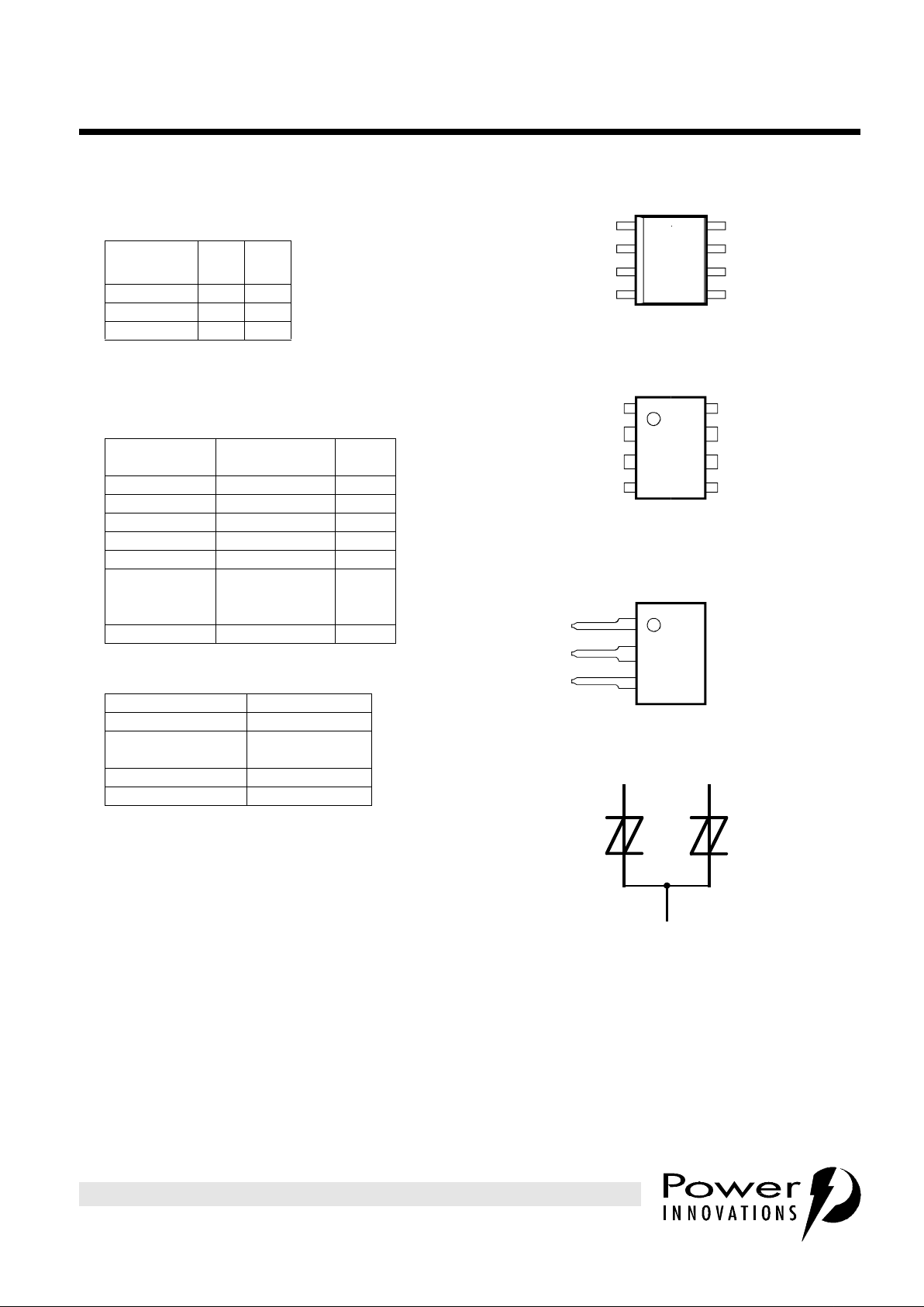
PACKAGE PART # SUFFIX
Small-outline D
Small-outline taped
and reeled
DR
Plastic DIP P
Single-in-line SL
crowbar. The high crowbar holding current
prevents d.c. latchup as the current subsides.
These monolithic protection devices are
fabricated in ion-implanted planar structures to
device symbol
G
T
R
Terminals T, R and G correspond to the
alternative line designators of A, B and C
SD3XAA
D PACKAGE
(TOP VIEW)
P PACKAGE
(TOP VIEW)
SL PACKAGE
(TOP VIEW)
MDXXAE
1
2
3
4
5
6
7
8 G
G
G
G
NC
T
R
NC
NC - No internal connection
1
2
3
4 5
6
7
8
R
G
T
G
T
G
G
R
Specified T terminal ratings require connection of pins 1 and 8.
Specified R terminal ratings require connection of pins 4 and 5.
MDXXAF
1
2
3
T
G
R
MDXXAG MD23AA
Page 2
TISP3125F3, TISP3150F3, TISP3180F3
DUAL SYMMETRICAL TRANSIENT
VOLTAGE SUPPRESSORS
2
MARCH 1994 - REVISED SEPTEMBER 1997
PRODUCT INFORMATION
ensure precise and matched breakover control and are virtually transparent to the system in normal operation
The small-outline 8-pin assignment has been carefully chosen for the TISP series to maximise the inter-pin
clearance and creepage distances which are used by standards (e.g. IEC950) to establish voltage withstand
ratings.
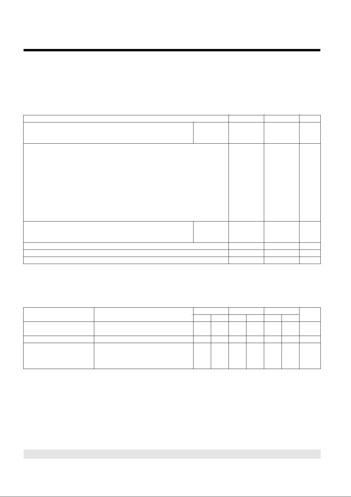
absolute maximum ratings
NOTES: 1. Further details on surge wave shapes are contained in the Applications Information section.
2. Initially the TISP must be in thermal equilibrium with 0°C < T
J
<70°C. The surge may be repeated after the TISP returns to its initial
conditions.
3. Above 70°C, derate linearly to zero at 150°C lead temperature.
NOTES: 4. These capacitance measurements employ a three terminal capacitance bridge incorporating a guard circuit. The third terminal is
connected to the guard terminal of the bridge.
5. Further details on capacitance are given in the Applications Information section.
† Typical value of the parameter, not a limit value.
RATING SYMBOL VALUE UNIT
Repetitive peak off-state voltage (0°C < T
J
< 70°C)
‘3125F3
‘3150F3
‘3180F3
V
DRM
± 100
± 120
± 145
V
Non-repetitive peak on-state pulse current(see Notes 1, 2 and 3)
I
TSP
A
1/2 µs(Gas tube differential transient, open-circuit voltage wave shape 1/2 µs) 350
2/10 µs(FCC Part 68, open-circuit voltage wave shape 2/10 µs) 175
8/20 µs(ANSI C62.41, open-circuit voltage wave shape 1.2/50 µs) 120
10/160 µs(FCC Part 68, open-circuit voltage wave shape 10/160 µs) 60
5/200 µs(VDE 0433, open-circuit voltage wave shape 2 kV, 10/700 µs) 50
0.5/310 µs(RLM 88, open-circuit voltage wave shape 1.5 kV, 0.5/700 µs) 38
5/310 µs(CCITT IX K17/K20, open-circuit voltage wave shape 2 kV, 10/700 µs) 50
5/310 µs(FTZ R12, open-circuit voltage wave shape 2 kV, 10/700 µs) 50
10/560 µs(FCC Part 68, open-circuit voltage wave shape 10/560 µs) 45
10/1000 µs(REA PE-60, open-circuit voltage wave shape 10/1000 µs) 35
Non-repetitive peak on-state current(see Notes 2 and 3) D Package
I
TSM
4
A rms50 Hz,1 s P Package 6
SL Package 6
Initial rate of rise of on-state current,Linear current ramp, Maximum ramp value < 38 A di
F
/dt 250 A/µs
Junction temperature T
J
-40 to +150 °C
Storage temperature range T
stg
-40 to +150 °C
electrical characteristics for the T and R terminals, TJ = 25°C
PARAMETER TEST CONDITIONS
TISP3125F3 TISP3150F3 TISP3180F3
UNIT
MIN MAX MIN MAX MIN MAX
I
DRM
Repetitive peak offstate current
V
D
= ±2V
DRM
, 0°C < TJ < 70°C ±10 ±10 ±10 µA
I
D
Off-state current VD= ±50 V ±10 ±10 ±10 µA
C
off
Off-state capacitance
f = 100 kHz,V
d
= 100 mV D Package
V
D
= 0, (see Notes 4 and 5) P Package
Third terminal = -50 to +50 V SL Package
50†
65†
30†
150
200
100
50†
65†
30†
150
200
100
50†
65†
30†
150
200
100
fF
description (Continued
)
Page 3
3
MARCH 1994 - REVISED SEPTEMBER 1997
TISP3125F3, TISP3150F3, TISP3180F3
DUAL SYMMETRICAL TRANSIENT
VOLTAGE SUPPRESSORS
PRODUCT INFORMATION
NOTES: 6 These capacitance measurements employ a three terminal capacitance bridge incorporating a guard circuit. The third terminal is
connected to the guard terminal of the bridge.
7. Further details on capacitance are given in the Applications Information section.
† Typical value of the parameter, not a limit value.
electrical characteristics for the T and G or the R and G terminals, TJ = 25°C
PARAMETER TEST CONDITIONS
TISP3125F3 TISP3150F3 TISP3180F3
UNIT
MIN MAX MIN MAX MIN MAX
I
DRM
Repetitive peak offstate current
V
D
= ±V
DRM
, 0°C < TJ < 70°C ±10 ±10 ±10 µA
V
(BO)
Breakover voltage
dv/dt = ±250 V/ms,
Source Resistance = 300 Ω
±125 ±150 ±180 V
V
(BO)
Impulse breakover voltage
dv/dt = ±1000 V/µs,di/dt < 20 A/µs
Source Resistance = 50
Ω
±139† ±164† ±194† V
I
(BO)
Breakover current
dv/dt = ±250 V/ms,
Source Resistance = 300
Ω
±0.15 ±0.6 ±0.15 ±0.6 ±0.15 ±0.6 A
V
T
On-state voltage IT= ±5 A,tW= 100 µs ±3 ±3 ±3 V
I
H
Holding current di/dt = -/+30 mA/ms ±0.15 ±0.15 ±0.15 A
dv/dt
Critical rate of rise of
off-state voltage
Linear voltage ramp,
Maximum ramp value < 0.85V
(BR)MIN
±5 ±5 ±5 kV/µs
I
D
Off-state current VD= ±50 V ±10 ±10 ±10 µA
C
off
Off-state capacitance
f = 100 kHz,V
d
= 100 mV VD= 0, 55† 95 55† 95 55† 95 pF
Third terminal = -50 to +50 V V
D
= -5 V 31† 50 31† 50 31† 50 pF
(see Notes 6 and 7) V
D
= -50 V 15† 25 15† 25 15† 25 pF
thermal characteristics
PARAMETER
MIN TYP MAX
UNIT
R
θJA
Junction to free air thermal resistance
D Package 160
°C/WP Package 100
SL Package 105
Page 4
TISP3125F3, TISP3150F3, TISP3180F3
DUAL SYMMETRICAL TRANSIENT
VOLTAGE SUPPRESSORS
4
MARCH 1994 - REVISED SEPTEMBER 1997
PRODUCT INFORMATION
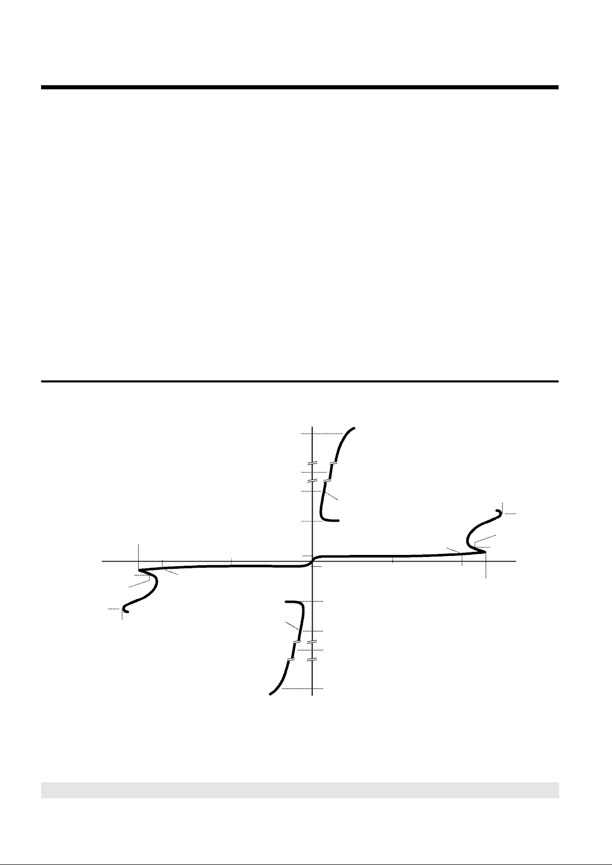
PARAMETER MEASUREMENT INFORMATION
Figure 1. VOLTAGE-CURRENT CHARACTERISTIC FOR ANY PAIR OF TERMINALS
.
-v
I
(BR)
V
(BR)
V
(BR)M
V
DRM
I
DRM
V
D
I
H
I
T
V
T
I
TSM
I
TSP
V
(BO)
I
(BO)
I
D
Quadrant I
Switching
Characteristic
+v
+i
V
(BO)
I
(BO)
I
(BR)
V
(BR)
V
(BR)M
V
DRM
I
DRM
V
D
I
D
I
H
I
T
V
T
I
TSM
I
TSP
-i
Quadrant III
Switching
Characteristic
PMXXAA
Page 5
5
MARCH 1994 - REVISED SEPTEMBER 1997
TISP3125F3, TISP3150F3, TISP3180F3
DUAL SYMMETRICAL TRANSIENT
VOLTAGE SUPPRESSORS
PRODUCT INFORMATION
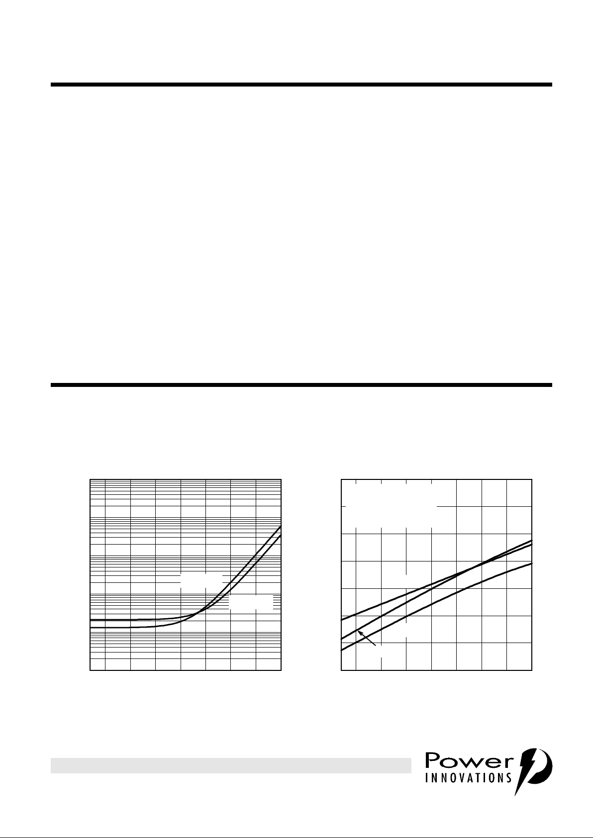
TYPICAL CHARACTERISTICS
T and G, or R and G terminals
Figure 2. Figure 3.
OFF-STATE CURRENT
TJ - Junction Temperature - °C
-25 0 25 50 75 100 125 150
I
D
- Off-State Current - µA
0·001
0·01
0·1
1
10
100
TC3MAF
JUNCTION TEMPERATURE
vs
VD = -50 V
VD = 50 V
NORMALISED BREAKDOWN VOLTAGES
TJ - Junction Temperature - °C
-25 0 25 50 75 100 125 150
Normalised Breakdown Voltages
0.9
1.0
1.1
1.2
TC3MAI
JUNCTION TEMPERA TURE
vs
V
(BO)
V
(BR)
V
(BR)M
Positive Polarity
Normalised to V
(BR)
I
(BR)
= 100 µA and 25°C
Page 6
TISP3125F3, TISP3150F3, TISP3180F3
DUAL SYMMETRICAL TRANSIENT
VOLTAGE SUPPRESSORS
6
MARCH 1994 - REVISED SEPTEMBER 1997
PRODUCT INFORMATION
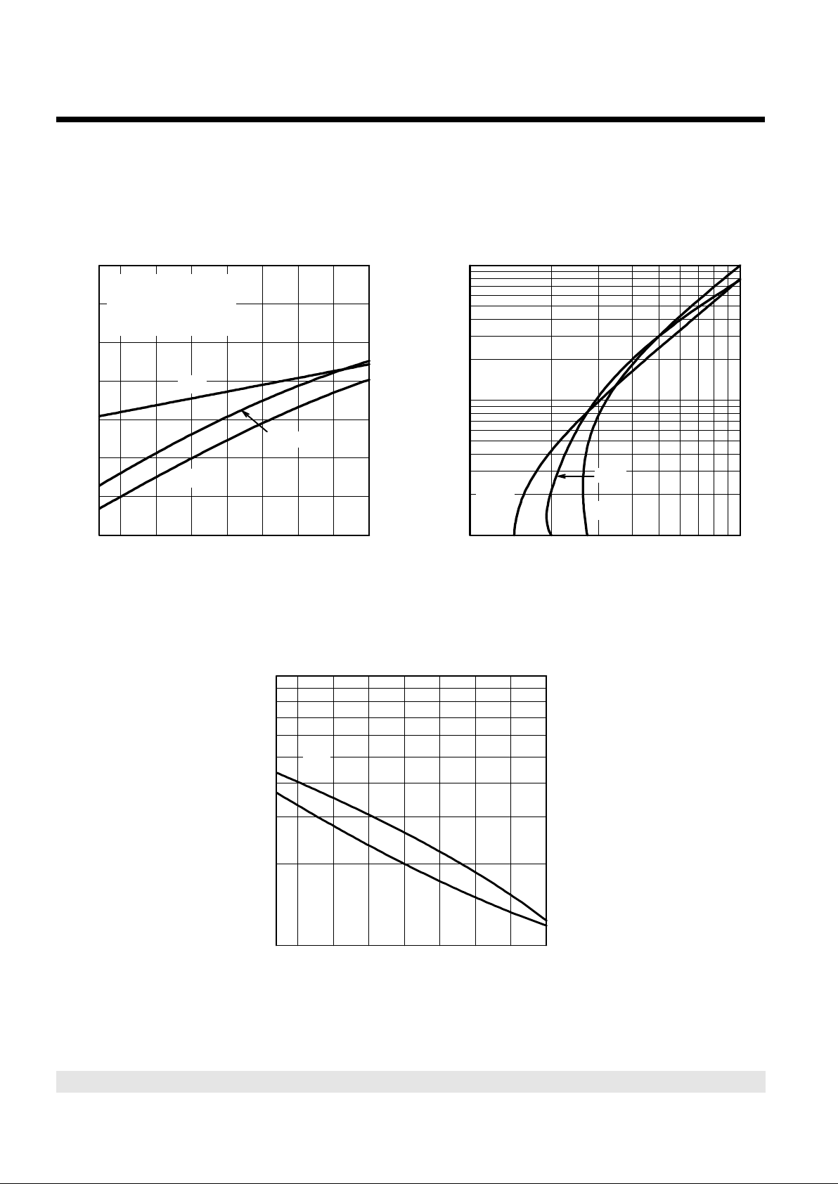
TYPICAL CHARACTERISTICS
T and G, or R and G terminals
Figure 4. Figure 5.
Figure 6.
NORMALISED BREAKDOWN VOLTAGES
TJ - Junction Temperature - °C
-25 0 25 50 75 100 125 150
Normalised Breakdown Voltages
0.9
1.0
1.1
1.2
TC3MAJ
JUNCTION TEMPERATURE
vs
V
(BO)
V
(BR)
V
(BR)M
Negative Polarity
Normalised to V
(BR)
I
(BR)
= 100 µA and 25°C
ON-STATE CURRENT
VT - On-State Voltage - V
2 3 4 5 6 7 8 91 10
I
T
- On-State Current - A
1
10
100
TC3MAL
ON-STATE VOLTAGE
vs
-40°C
150°C
25°C
HOLDING CURRENT & BREAKOVER CURRENT
TJ - Junction Temperature - °C
-25 0 25 50 75 100 125 150
I
H
, I
(BO)
- Holding Current, Breakover Current - A
0.2
0.3
0.4
0.5
0.6
0.7
0.8
0.9
0.1
1.0
TC3MAH
JUNCTION TEMPERATURE
vs
I
(BO)
I
H
Page 7

7
MARCH 1994 - REVISED SEPTEMBER 1997
TISP3125F3, TISP3150F3, TISP3180F3
DUAL SYMMETRICAL TRANSIENT
VOLTAGE SUPPRESSORS
PRODUCT INFORMATION
TYPICAL CHARACTERISTICS
T and G, or R and G terminals
Figure 7. Figure 8.
Figure 9.
NORMALISED B REAKOVER VOLTAGE
di/dt - Rate of Rise of Principle Current - A/µs
0·001 0·01 0·1 1 10 100
Normalised Breakover Voltage
1.0
1.1
1.2
1.3
TC3MAB
Positive
RATE OF RISE OF PRINCIPLE CURRENT
vs
Negative
OFF-STATE CAPACITANCE
Terminal Voltage - V
0·1 1 10
Off-State Capacitance - pF
10
100
TC3MAE
50
TERMINA L VOLTAGE
vs
Positive Bias
Negative Bias
OFF-STATE CAPACITANCE
TJ - Junction Temperature - °C
-25 0 25 50 75 100 125 150
Off-State Capacitance - pF
10
100
TC3MAD
JUNCTION TEMPERATURE
vs
500
Terminal Bias = 0
Terminal Bias = 50 V
Terminal Bias = -50 V
Page 8

TISP3125F3, TISP3150F3, TISP3180F3
DUAL SYMMETRICAL TRANSIENT
VOLTAGE SUPPRESSORS
8
MARCH 1994 - REVISED SEPTEMBER 1997
PRODUCT INFORMATION
TYPICAL CHARACTERISTICS
T and G, or R and G terminals
Figure 10.
TYPICAL CHARACTERISTICS
T and R terminals
Figure 11. Figure 12.
SURGE CURRENT
Decay Time - µs
10 100 1000
Maximum Surge Current - A
10
100
1000
TC3MAA
vs
DECAY TIME
2
OFF-STATE CURRENT
TJ - Junction Temperature - °C
-25 0 25 50 75 100 125 150
I
D
- Off-State Current - µA
0·001
0·01
0·1
1
10
100
TC3MAG
JUNCTION TEMPERATURE
vs
VD = ±50 V
NORMALISED BREAKDOWN VOLTAGES
TJ - Junction Temperature - °C
-25 0 25 50 75 100 125 150
Normalised Breakdown Voltages
0.9
1.0
1.1
1.2
TC3MAK
JUNCTION TEMPERA TURE
vs
V
(BO)
V
(BR)
V
(BR)M
Both Polarities
Normalised to V
(BR)
I
(BR)
= 100 µA and 25°C
Page 9

9
MARCH 1994 - REVISED SEPTEMBER 1997
TISP3125F3, TISP3150F3, TISP3180F3
DUAL SYMMETRICAL TRANSIENT
VOLTAGE SUPPRESSORS
PRODUCT INFORMATION
TYPICAL CHARACTERISTICS
T and R terminals
Figure 13. Figure 14.
THERMAL INFORMATION
Figure 15. Figure 16.
NORMALISED B REAKOVER VOLTAGE
di/dt - Rate of Rise of Principle Current - A/µs
0·001 0·01 0·1 1 10 100
Normalised Breakover Voltage
1.0
1.1
1.2
1.3
TC3MAC
RATE OF RISE OF PRINCIPLE CURRENT
vs
OFF-STATE CAPACITANCE
Terminal Voltage - V
0·1 1 10
Off-State Capacitance - fF
20
30
40
50
60
70
80
90
10
100
TC3XAA
50
TERMINAL VOLTAGE
vs
D Package
P Package
SL Package
Both Voltage Polarities
MAXIMUM NON-RECURRING 50 Hz CURRENT
t - Current Duration - s
0·1 1 10 100 1000
I
TRMS
- Maximum Non-Recurrent 50 Hz Current - A
1
10
vs
CURRENT DURATION
D Package
SL Package
TI3MAB
P Package
V
GEN
= 250 Vrms
R
GEN
= 10 to 150 ΩΩ
THERMAL RESPONSE
t - Power Pulse Duration - s
0·0001 0·001 0·01 0·1 1 10 100 1000
Z
θ
θJ
Α
Α
- Transient Thermal Impedance - °C/W
1
10
100
D Package
P Package
SL Package
TI3MAA
Page 10

TISP3125F3, TISP3150F3, TISP3180F3
DUAL SYMMETRICAL TRANSIENT
VOLTAGE SUPPRESSORS
10
MARCH 1994 - REVISED SEPTEMBER 1997
PRODUCT INFORMATION
electrical characteristics
The electrical characteristics of a TISP are strongly dependent on junction temperature, TJ. Hence a
characteristic value will depend on the junction temperature at the instant of measurement. The values given
in this data sheet were measured on commercial testers, which generally minimise the temperature rise
caused by testing. Application values may be calculated from the parameters’ temperature curves, the power
dissipated and the thermal response curve (Zθ).
lightning surge
wave shape notation
Most lightning tests, used for equipment verification, specify a unidirectional sawtooth waveform which has an
exponential rise and an exponential decay. Wave shapes are classified in terms of peak amplitude (voltage
or current), rise time and a decay time to 50% of the maximum amplitude. The notation used for the wave
shape is amplitude, rise time/decay time. A 50A, 5/310 µs wave shape would have a peak current value of
50 A, a rise time of 5 µs and a decay time of 31 0 µs. The TISP surge current graph comprehends the wave
shapes of commonly used surges.
generators
There are three categories of surge generator type, single wave shape, combination wave shape and circuit
defined. Single wave shape generators have essentially the same wave shape for the open circuit voltage
and short circuit current (e.g. 10/1000 µs open circuit voltage and short circuit current). Combination
generators have two wave shapes, one for the open circuit voltage and the other for the short circuit current
(e.g. 1.2/50 µs open circuit voltage and 8/20 µs short circuit current) Circuit specified generators usually
equate to a combination generator, although typically only the open circuit voltage waveshape is referenced
(e.g. a 10/700 µs open circuit voltage generator typically produces a 5/310 µs short circuit current). If the
combination or circuit defined generators operate into a finite resistance the wave shape produced is
intermediate between the open circuit and short circuit values.
current rating
When the TISP switches into the on-state it has a very low impedance. As a result, although the surge wave
shape may be defined in terms of open circuit voltage, it is the current wave shape that must be used to
assess the required TISP surge capability. As an example, the CCITT IX K17 1.5 kV, 10/700 µs surge is
changed to a 38 A, 5/310 µs waveshape when driving into a short circuit. Thus the TISP surge current
capability, when directly connected to the generator, will be found for the CCITT IX K17 waveform at 310 µs
on the surge graph and not 700 µs. Some common short circuit equivalents are tabulated below:
Any series resistance in the protected equipment will reduce the peak circuit current to less than the
generators’ short circuit value. A 2 kV open circuit voltage, 50 A short circuit current generator has an
effective output impedance of 40 Ω (2000/50). If the equipment has a series resistance of 25 Ω then the
surge current requirement of the TISP becomes 31 A (2000/65) and not 50 A.
APPLICATIONS INFORMATION
STANDARD OPEN CIRCUIT
VOLTAGE
SHORT CIRCUIT
CURRENT
CCITT IX K17 1.5 kV, 10/700 µs 38 A, 5/310 µs
CCITT IX K20 1 kV, 10/700 µs 25 A, 5/310 µs
RLM88 1.5 kV, 0.5/700 µ s 38 A, 0.2/310 µs
VDE 0433 2.0 kV, 10/700 µs 50 A, 5/200 µs
FTZ R12 2.0 kV, 10/700 µ s 50 A, 5/310 µs
Page 11

11
MARCH 1994 - REVISED SEPTEMBER 1997
TISP3125F3, TISP3150F3, TISP3180F3
DUAL SYMMETRICAL TRANSIENT
VOLTAGE SUPPRESSORS
PRODUCT INFORMATION
protection voltage
The protection voltage, (V
(BO)
), increases under lightning surge conditions due to thyristor regeneration. This
increase is dependent on the rate of current rise, di/dt, when the TISP is clamping the voltage in its
breakdown region. The V
(BO)
value under surge conditions can be estimated by multiplying the 50 Hz rate
V
(BO)
(250 V/ms) value by the normalised increase at the surge’s di/dt (Figure 7.) . An estimate of the di/dt
can be made from the surge generator voltage rate of rise, dv/dt, and the circuit resistance.
As an example, the CCITT IX K17 1.5 kV, 10/700 µs surge has an average dv/dt of 150 V/µs, but, as the rise
is exponential, the initial dv/dt is higher, being in the region of 450 V/µs. The instantaneous generator output
resistance is 25 Ω. If the equipment has an additional series resistance of 20 Ω, the total series resistance
becomes 45 Ω. The maximum di/dt then can be estimated as 450/45 = 10 A/µs. In practice the
measureddi/dt and protection voltage increase will be lower due to inductive effects and the finite slope
resistance of the TISP breakdown region.
capacitance
off-state capacitance
The off-state capacitance of a TISP is sensitive to junction temperature, TJ, and the bias voltage, comprising
of the dc voltage, V
D
, and the ac voltage, Vd. All the capacitance values in this data sheet are measured with
an ac voltage of 100 mV. The typical 25°C variation of capacitance value with ac bias is shown in Figure 17.
When V
D
>> Vd the capacitance value is independent on the value of Vd. The capacitance is essentially
constant over the range of normal telecommunication frequencies.
Figure 17.
APPLICATIONS INFORMATION
NORMALISED CAPACITANCE
Vd - RMS AC Test Voltage - mV
1 10 100 1000
Normalised Capacitance
0.70
0.75
0.80
0.85
0.90
0.95
1.00
1.05
AIXXAA
Normalised to Vd = 100 mV
DC Bias, VD = 0
RMS AC TEST VOLTAGE
vs
Page 12

TISP3125F3, TISP3150F3, TISP3180F3
DUAL SYMMETRICAL TRANSIENT
VOLTAGE SUPPRESSORS
12
MARCH 1994 - REVISED SEPTEMBER 1997
PRODUCT INFORMATION
longitudinal balance
Figure 18 shows a three terminal TISP with its equivalent "delta" capacitance Each capacitance, CTG, C
RG
and CTR, is the true terminal pair capacitance measured with a three terminal or guarded capacitance bridge.
If wire R is biased at a larger potential than wire T then C
TG
> CRG. Capacitance CTG is equivalent to a
capacitance of C
RG
in parallel with the capacitive difference of (CTG- CRG). The line capacitive unbalance is
due to (C
TG
- CRG) and the capacitance shunting the line is CTR+ CRG/2 .
Figure 18.
All capacitance measurements in this data sheet are three terminal guarded to allow the designer to
accurately assess capacitive unbalance effects. Simple two terminal capacitance meters (unguarded third
terminal) give false readings as the shunt capacitance via the third terminal is included.
APPLICATIONS INFORMATION
Page 13

13
MARCH 1994 - REVISED SEPTEMBER 1997
TISP3125F3, TISP3150F3, TISP3180F3
DUAL SYMMETRICAL TRANSIENT
VOLTAGE SUPPRESSORS
PRODUCT INFORMATION
D008
plastic small-outline package
This small-outline package consists of a circuit mounted on a lead frame and encapsulated within a plastic
compound. The compound will withstand soldering temperature with no deformation, and circuit performance
characteristics will remain stable when operated in high humidity conditions. Leads require no additional
cleaning or processing when used in soldered assembly.
MECHANICAL DATA
5,21 (0.205)
4,60 (0.181)
NOTES: A. Leads are within 0,25 (0.010) radius of true position at maximum material condition.
B. Body dimensions do not include mold flash or protrusion.
C. Mold flash or protrusion shall not exceed 0,15 (0.006).
D. Lead tips to be planar within ±0,051 (0.002).
1,75 (0.069)
1,35 (0.053)
6,20 (0.244)
5,80 (0.228)
5,00 (0.197)
4,80 (0.189)
D008
8
7 6 5
432
1
4,00 (0.157)
3,81 (0.150)
7° NOM
3 Places
7° NOM
4 Places
0,51 (0.020)
0,36 (0.014)
8 Places
Pin Spacing
1,27 (0.050)
(see Note A)
6 Places
1,12 (0.044)
0,51 (0.020)
4° ± 4°
0,79 (0.031)
0,28 (0.011)
0,203 (0.008)
0,102 (0.004)
ALL LINEAR DIMENSIONS ARE IN MILLIMETERS AND PARENTHETICALLY IN INCHES
Designation per JEDEC Std 30:
PDSO-G8
0,50 (0.020)
0,25 (0.010)
x 45°NOM
0,229 (0.0090)
0,190 (0.0075)
MDXXAA
Page 14

TISP3125F3, TISP3150F3, TISP3180F3
DUAL SYMMETRICAL TRANSIENT
VOLTAGE SUPPRESSORS
14
MARCH 1994 - REVISED SEPTEMBER 1997
PRODUCT INFORMATION
P008
plastic dual-in-line package
This dual-in-line package consists of a circuit mounted on a lead frame and encapsulated within a plastic
compound. The compound will withstand soldering temperature with no deformation, and circuit performance
characteristics will remain stable when operated in high humidity conditions The package is intended for
insertion in mounting-hole rows on 7,62 (0.300) centers. Once the leads are compressed and inserted,
sufficient tension is provided to secure the package in the board during soldering. Leads require no
additional cleaning or processing when used in soldered assembly.
MECHANICAL DATA
1 2 3 4
8
7 6 5
10,2 (0.400) MAX
Index
Dot
1,78 (0.070) MAX
4 Places
5,08 (0.200)
MAX
0,51 (0.020)
MIN
2,54 (0.100) T.P.
6 Places
(see Note A)
0,533 (0.021)
0,381 (0.015)
8 Places
3,17 (0.125)
MIN
Seating
Plane
0,36 (0.014)
0,20 (0.008)
8 Places
105°
90°
8 Places
6,60 (0.260)
6,10 (0.240)
7,87 (0.310)
7,37 (0.290)
T.P.
C
L
C
L
ALL LINEAR DIMENSIONS ARE IN MILLIMETERS AND PARENTHETICALLY IN INCHES
P008
Designation per JEDEC Std 30:
PDIP-T8
NOTE A: Each pin centerline is located within 0,25 (0.010) of its true longitudinal position
MDXXABA
Page 15

15
MARCH 1994 - REVISED SEPTEMBER 1997
TISP3125F3, TISP3150F3, TISP3180F3
DUAL SYMMETRICAL TRANSIENT
VOLTAGE SUPPRESSORS
PRODUCT INFORMATION
SL003
3-pin plastic single-in-line package
This single-in-line package consists of a circuit mounted on a lead frame and encapsulated within a plastic
compound. The compound will withstand soldering temperature with no deformation, and circuit performance
characteristics will remain stable when operated in high humidity conditions. Leads require no additional
cleaning or processing when used in soldered assembly.
MECHANICAL DATA
NOTES: A. Each pin centerline is located within 0,25 (0.010) of its true longitudinal position.
B. Body molding flash of up to 0,15 (0.006) may occur in the package lead plane.
1,854 (0.073) MAX
0,711 (0.028)
0,559 (0.022)
3 Places
1 2 3
Pin Spacing
2,54 (0.100) T.P.
(see Note A)
2 Places
12,9 (0.492)
MAX
4,57 (0.180)
MAX
6,60 (0.260)
6,10 (0.240)
0,356 (0.014)
0,203 (0.008)
3 Places
SL003
10,2 (0.400) MAX
8,31 (0.327)
MAX
4,267 (0.168)
MIN
ALL LINEAR DIMENSIONS ARE IN MILLIMETERS AND PARENTHETICALLY IN INCHES
Index
Dot
MDXXAD
Page 16

TISP3125F3, TISP3150F3, TISP3180F3
DUAL SYMMETRICAL TRANSIENT
VOLTAGE SUPPRESSORS
16
MARCH 1994 - REVISED SEPTEMBER 1997
PRODUCT INFORMATION
D008
tape dimensions
MECHANICAL DATA
D008 Package (8 pin SOIC) Single-Sprocket Tape
ALL LINEAR DIMENSIONS IN MILLIMETERS
6,30
6,50
11,70
12,305,45
5,55
1,50
1,60
3,90
4,10
7,95
8,05
1,95
2,05
0,8 MIN.
0 MIN.
0,40
2,0
2,2
Direction of Feed
ø 1,5 MIN.
Carrier Tape
Embossment
Cover
Tape
MDXXAT
NOTES: A. Taped devices are supplied on a reel of the following dimensions: Reel diameter: 330 +0,0/-4,0 mm
Reel hub diameter: 100 ±2,0 mm
Reel axial hole: 13,0 ±0,2 mm
B. 2500 devices are on a reel.
Page 17

17
MARCH 1994 - REVISED SEPTEMBER 1997
TISP3125F3, TISP3150F3, TISP3180F3
DUAL SYMMETRICAL TRANSIENT
VOLTAGE SUPPRESSORS
PRODUCT INFORMATION
IMPORTANT NOTICE
Power Innovations Limited (PI) reserves the right to make changes to its products or to discontinue any
semiconductor product or service without notice, and advises its customers to verify, before placing orders, that the
information being relied on is current.
PI warrants performance of its semiconductor products to the specifications applicable at the time of sale in
accordance with PI's standard warranty. Testing and other quality control techniques are utilized to the extent PI
deems necessary to support this warranty. Specific testing of all parameters of each device is not necessarily
performed, except as mandated by government requirements.
PI accepts no liability for applications assistance, customer product design, software performance, or infringement
of patents or services described herein. Nor is any license, either express or implied, granted under any patent
right, copyright, design right, or other intellectual property right of PI covering or relating to any combination,
machine, or process in which such semiconductor products or services might be or are used.
PI SEMICONDUCTOR PRODUCTS ARE NOT DESIGNED, INTENDED, AUTHORIZED, OR WARRANTED TO BE
SUITABLE FOR USE IN LIFE-SUPPORT APPLICATIONS, DEVICES OR SYSTEMS.
Copyright © 1997, Power Innovations Limited
 Loading...