

Page 1
TIP142T
®
COMPLEMENTARY SILICON POWER
■ STMicroelectronics P REF ERRED
SALESTYPES
■ COMPLEMENTARY PNP - NPN DEVICES
■ MONOLI THIC D A RLING TO N
CONFIGU R ATIO N
■ LOW VOLTAGE
■ HIGH CURRENT
■ HIGH GAI N
APPLICATIONS
■ GENERAL PURPOSE SWITCHING
DESCRIPTION
The TIP142T is a silicon Epitaxial-Base NPN
power transistor in monolithic Darlington
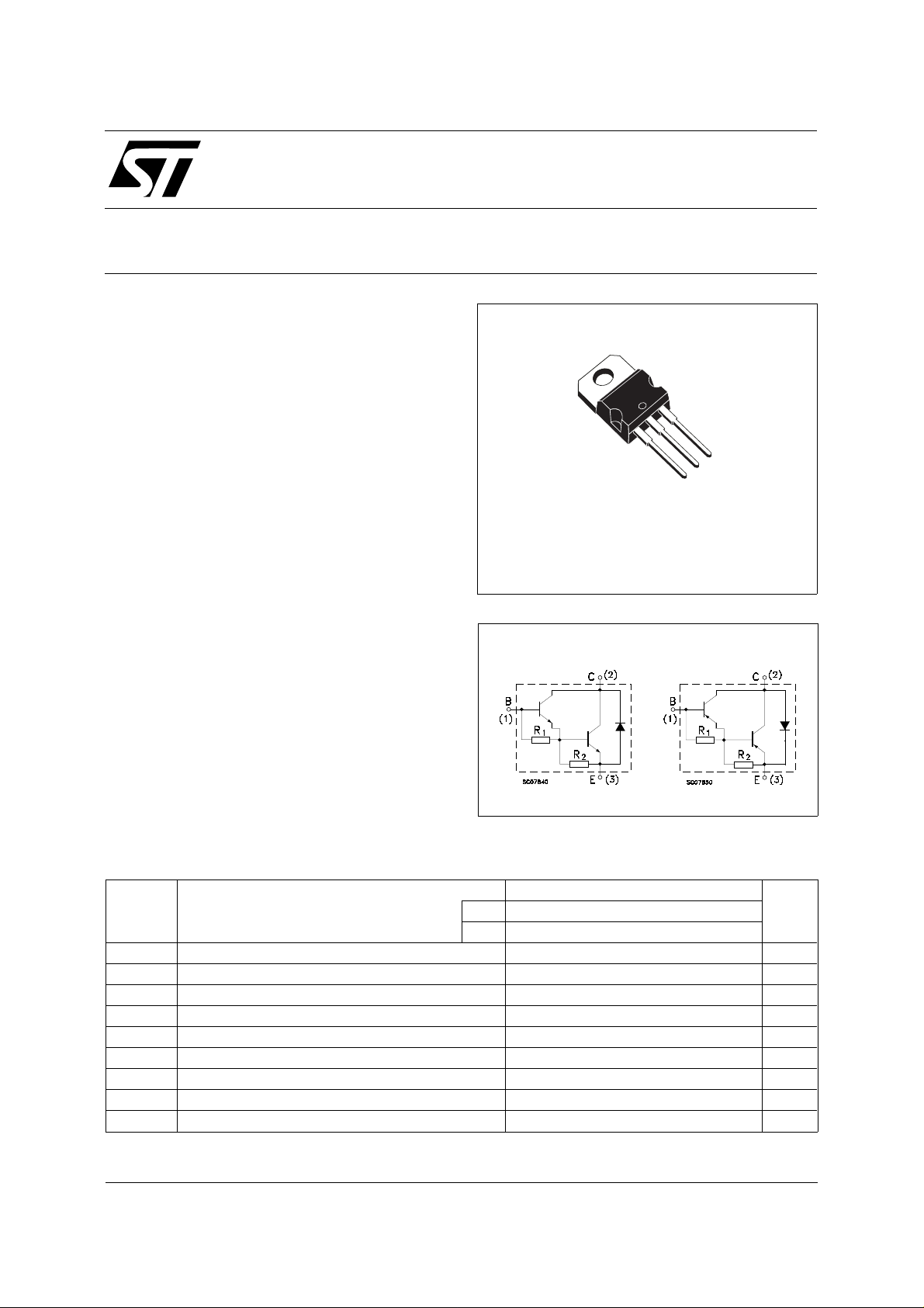
configuration, mounted in TO-220 plastic
package. It is intented for use in power linear and
switching applications.
The complementary PNP type is TIP147T .
TIP147T
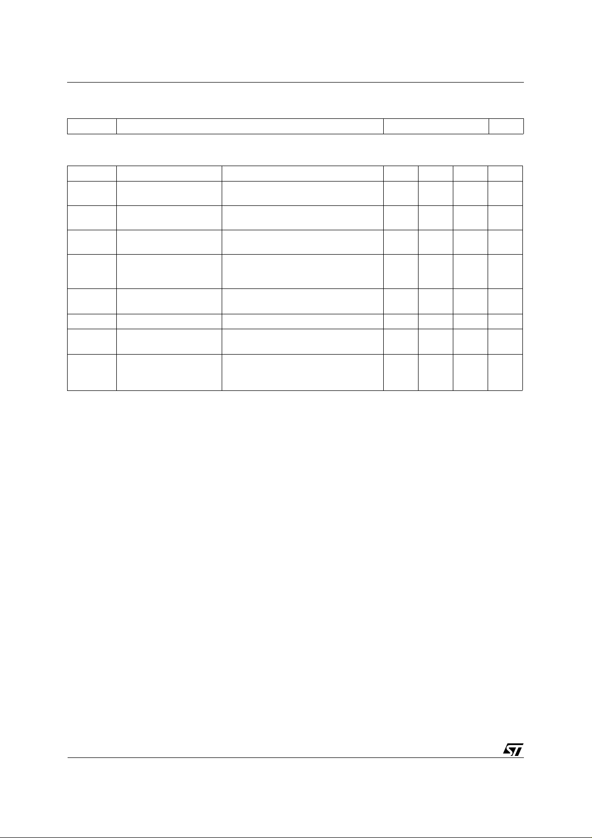
DARLINGTON TRANSISTORS
3
2
1
TO-220
INTER NAL SCH E M ATI C DIAG RA M
ABSOLUTE MAXIMUM RATINGS
Symbol Parameter Value Unit
NPN TIP142T
PNP TIP147T
V
V
V
I
P
T
For PNP types voltage and current values are negative.
March 2000
Collector-Base Voltage (IE = 0) 100 V
CBO
Collector-Emitter Voltage (IB = 0) 100 V
CEO
Emitter-Base Voltage (IC = 0) 5 V
EBO
I
Collector Current 15 A
C
Collector Peak Current (tp < 5ms) 20 A
CM
Base Current 0.5 A
I
B
Total Dissipation at T
tot
Storage Temperature - 65 to 150
stg
T
Max. Operating Junction Temperature 150
j
case
≤ 25 oC
90 W
o
C
o
C
1/4
Page 2
TIP142T / TIP147T
THERMAL DATA
R
thj-case
Thermal Resistance Junction-case Max 1.38
o
C/W
ELECTRICAL CHARACTERISTICS (T
= 25 oC unless otherwise specified)
case
Symbol Parameter Test Conditions Min. Typ. Max. Unit
I
CBO
I
CEO
I
EBO
V
CEO(sus)
Collector Cut-off
Current (I
= 0)
E
Collector Cut-off
Current (I
= 0)
B
Emitter Cut-off Current
(I
= 0)
C
* Collector-Emitter
= 100 V 1 mA
V
CB
= 50 V 2 mA
V
CE
= 5 V 2 mA
V
EB
I
= 30 mA 100 V
C
Sustaining Voltage
(I
= 0)
B
V
* Collector-Emitter
CE(sat)
Saturation Voltage
V
* Base-Emitter Voltage IC =10 A VCE = 4 V 3 V
BE(on)
h
* DC Current Gain IC = 5 A VCE = 4 V
FE
IC = 5 A IB = 10 mA
I
= 10 A IB = 40 mA
C
I
= 10 A VCE = 4 V
C
2
3
1000
500
RESISTIVE LOAD
t
t
For PNP types voltage and current values are negative.
∗ Pulsed: Pulse duration = 300 µs, duty cycle 1.5 %.
on
off
Turn-on Time
Turn-off Time
I
= 10 A IB1 = 10 mA
C
= -40 mA RL = 3 Ω
I
B2
0.9
4
V
V
µs
µs
2/4
Page 3

TO-220 MECHANICAL DATA
TIP142T / TIP147T
DIM.
MIN. TYP. MAX. MIN. TYP. MAX.
A 4.40 4.60 0.173 0.181
C 1.23 1.32 0.048 0.051
D 2.40 2.72 0.094 0.107
D1 1.27 0.050
E 0.49 0.70 0.019 0.027
F 0.61 0.88 0.024 0.034
F1 1.14 1.70 0.044 0.067
F2 1.14 1.70 0.044 0.067
G 4.95 5.15 0.194 0.203
G1 2.4 2.7 0.094 0.106
H2 10.0 10.40 0.393 0.409
L2 16.4 0.645
L4 13.0 14.0 0.511 0.551
L5 2.65 2.95 0.104 0.116
L6 15.25 15.75 0.600 0.620
L7 6.2 6.6 0.244 0.260
L9 3.5 3.93 0.137 0.154
DIA. 3.75 3.85 0.147 0.151
mm inch
P011C
3/4
Page 4

TIP142T / TIP147T
Information furnished is believed to be accurate and reliable. However, STMicroelectronics assumes no responsibility for the consequences
of use of such inform ation nor for any infringe ment o f patents or other rig hts o f third par ties which ma y resul t from i ts use. N o li cen se is
granted by implicatio n or otherwise under any patent or patent rights of STMicroelectronics. Specification mentioned in this publication are
subject to change without notice. This publication supersedes and replaces all information previously supplied. STMicroelectronics products
are not authorized for use as critical compo nents in life support devices or systems without express written approval of STMicroelectronics.
The ST logo is a trademark of STMicroelectronics
© 2000 STMicroelectro nics – Printed in Italy – All Rights Reserved
STMicroelectronics GROUP OF COMPANIES
Australia - Brazil - China - Finland - France - Germany - Hong Kong - India - Italy - Japan - Malaysia - Malta - Morocco -
Singapore - Spain - Sweden - Switzerland - United Kingdom - U.S.A.
http://www.st.com
4/4
 Loading...