

Page 1
TICP206 SERIES
SILICON TRIACS
Copyright © 1997, Power Innovations Limited, UK
● 1.5 A RMS
MARCH 1988 - REVISED MARCH 1997
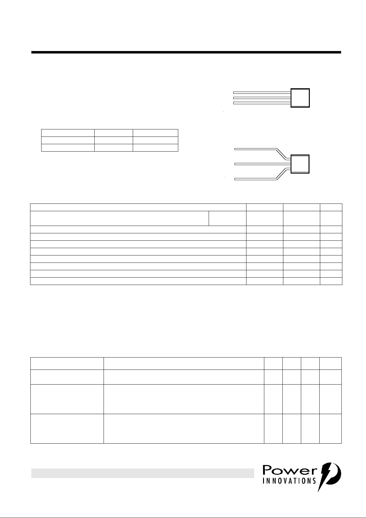
LP PACKAGE
(TOP VIEW)
● Glass Passivated Wafer
● 400 V to 600 V Off-State Voltage
● Max I
of 10 mA
GT
G
MT2
MT1
1
2
3
● Package Options
PACKAGE PACKING PART # SUFFIX
LP Bulk (None)
LP with fomed leads Tape and Reel R
G
MT2
LP PACKAGE
WITH FORMED LEADS
(TOP VIEW)
1
2
3
MT1
absolute maximum ratings over operating case temperature (unless otherwise noted)
RATING SYMBOL VALUE UNIT
Repetitive peak off-state voltage (see Note 1)
Full-cycle RMS on-state current at (or below) 85°C case temperature (see Note 2) I
Peak on-state surge current full-sine-wave (see Note 3) I
Peak on-state surge current half-sine-wave (see Note 4) I
Peak gate current I
Average gate power dissipation at (or below) 85°C case temperature (see Note 5) P
Operating case temperature range T
Storage temperature range T
Lead temperature 1.6 mm from case for 10 seconds T
TICP206D
TICP206M
V
DRM
T(RMS)
TSM
TSM
GM
G(AV)
C
stg
L
NOTES: 1. These values apply bidirectionally for any value of resistance between the gate and Main Terminal 1.
2. This value applies for 50-Hz full-sine-wave operation with resistive load. Above 85°C derate linearly to 110°C case temperature at
the rate of 60 mA/°C.
3. This value applies for one 50-Hz full-sine-wave when the device is operating at (or below) the rated value of on-state current.
Surge may be repeated after the device has returned to original thermal equilibrium. During the surge, gate control may be lost.
4. This value applies for one 50-Hz half-sine-wave when the device is operating at (or below) the rated value of on-state current.
Surge may be repeated after the device has returned to original thermal equilibrium. During the surge, gate control may be lost.
5. This value applies for a maximum averaging time of 20 ms.
400
600
1.5 A
10 A
12 A
±0.2 A
0.3 W
-40 to +110 °C
-40 to +125 °C
230 °C
MDC2AA
MDC2AB
V
electrical characteristics at 25°C case temperature (unless otherwise noted)
PARAMETER TEST CONDITIONS
I
DRM
I
GTM
V
GTM
Repetitive peak offstate current
Peak gate trigger
current
Peak gate trigger
voltage
= rated V
V
D
V
supply
V
supply
V
supply
V
supply
V
supply
V
supply
V
supply
V
supply
DRM
= +12 V†
= +12 V†
= -12 V†
= -12 V†
= +12 V†
= +12 V†
= -12 V†
= -12 V†
IG = 0 ±20 µA
R
= 10 Ω
L
RL = 10 Ω
RL = 10 Ω
RL = 10 Ω
R
= 10 Ω
L
RL = 10 Ω
RL = 10 Ω
RL = 10 Ω
t
t
t
t
t
t
t
t
p(g)
p(g)
p(g)
p(g)
p(g)
p(g)
p(g)
p(g)
> 20 µs
> 20 µs
> 20 µs
> 20 µs
> 20 µs
> 20 µs
> 20 µs
> 20 µs
† All voltages are with respect to Main Terminal 1.
PRODUCT INFORMATION
Information is current as of publication date. Products conform to specifications in accordance
with the terms of Power Innovations standard warranty. Production processing does not
necessarily include testing of all parameters.
MIN TYP MAX
8
-8
-8
10
2.5
-2.5
-2.5
2.5
UNIT
mA
V
1
Page 2
TICP206 SERIES
SILICON TRIACS
MARCH 1988 - REVISED MARCH 1997
electrical characteristics at 25°C case temperature (unless otherwise noted) (continued)
PARAMETER TEST CONDITIONS
V
TM
I
H
I
L
Peak on-state
voltage
Holding current
Latching current
= ±1 A IG = 50 mA (see Note 6) ±2.2 V
I
TM
V
V
V
V
supply
supply
supply
supply
= +12 V†
= -12 V†
= +12 V†
= -12 V†
I
= 0
G
= 0
I
G
(see Note 7)
† All voltages are with respect to Main Terminal 1.
NOTES: 6. This parameter must be measured using pulse techniques, t
the current carrying contacts are located within 3.2 mm from the device body.
7. The triacs are triggered by a 15-V (open circuit amplitude) pulse supplied by a generator with the following characteristics:
= 100 Ω, t
R
G
= 20 µs, tr = ≤ 15 ns, f = 1 kHz.
p(g)
MIN TYP MAX
Init’ I
= 100 mA
TM
= -100 mA
Init’ I
TM
= ≤ 1 ms, duty cycle ≤ 2 %. Voltage-sensing contacts separate from
p
30
-30
40
-40
UNIT
mA
mA
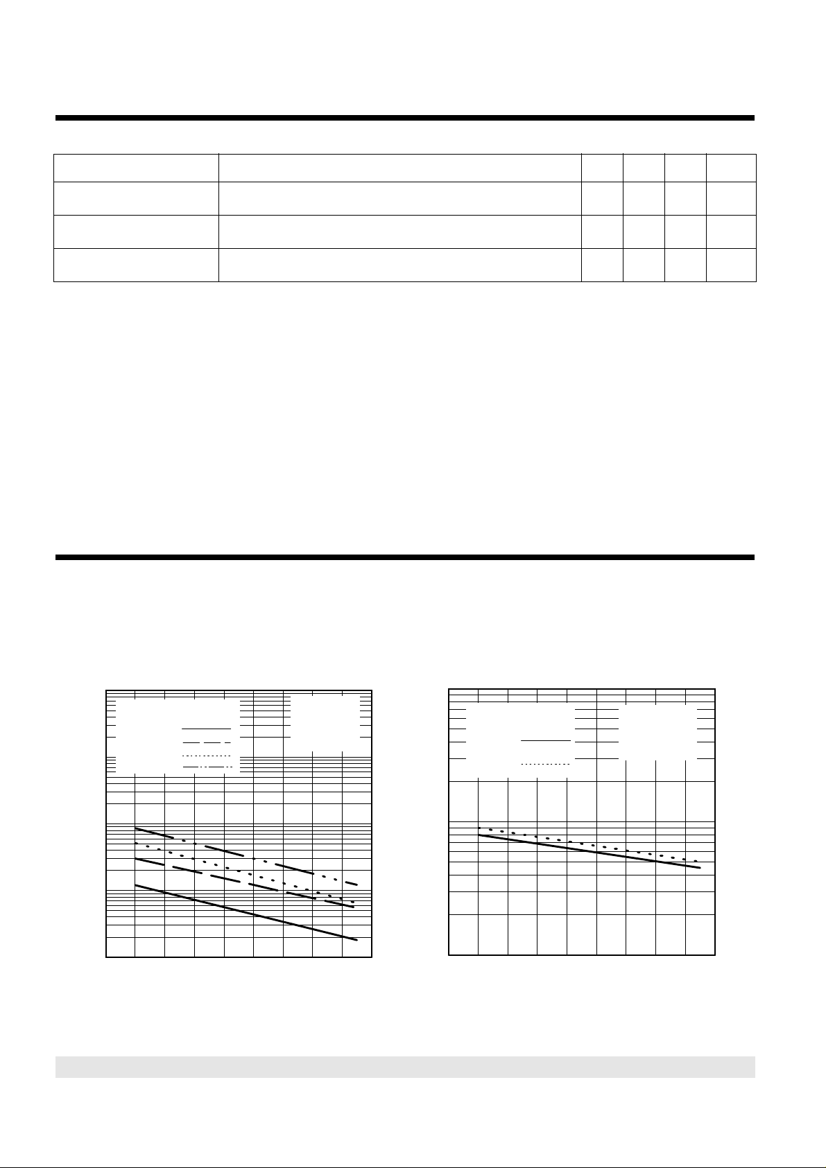
TYPICAL CHARACTERISTICS
GATE TRIGGER CURRENT
vs
TEMPERATURE
1000
V
supply IGTM
+ +
+ -
100
- -
- +
10
- Gate Trigger Current - mA
GT
1
I
0·1
-60 -40 -20 0 20 40 60 80 100 120
TC - Case Temperature - °C
Figure 1. Figure 2.
VAA = ± 12 V
RL = 10 ΩΩ
t
p(g)
TC05AA
= 20 µs
GATE TRIGGER VOLTAGE
vs
TEMPERATURE
10
V
supply IGTM
+ +
}
+ -
- }
- +
1
- Gate Trigger Voltage - V
GT
V
0·1
-60 -40 -20 0 20 40 60 80 100 120
TC - Case Temperature - °C
VAA = ± 12 V
RL = 10 ΩΩ
t
= 20 µs
p(g)
TC05AB
PRODUCT INFORMATION
2
Page 3
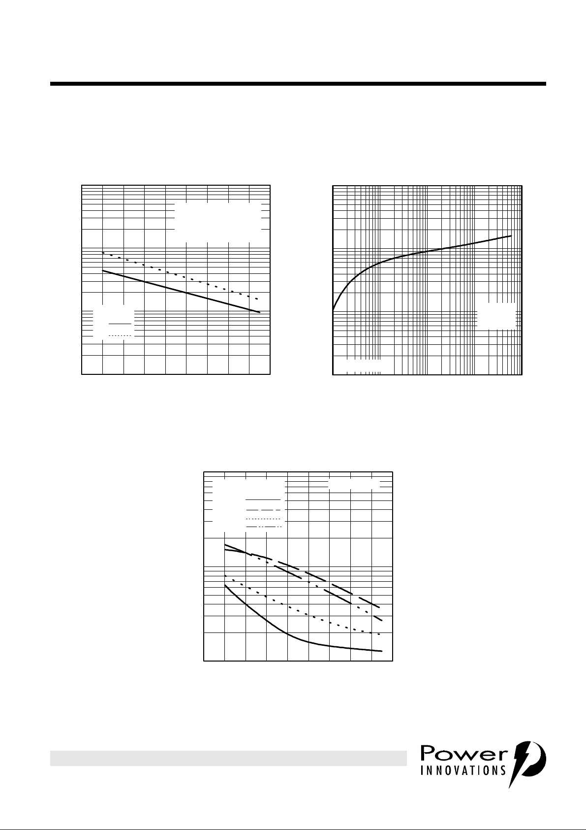
TYPICAL CHARACTERISTICS
TICP206 SERIES
SILICON TRIACS
MARCH 1988 - REVISED MARCH 1997
HOLDING CURRENT
vs
CASE TEMPERATURE
100
VAA = ± 12 V
IG = 0
Initiating ITM = 100 mA
10
V
1
- Holding Current - mA
H
I
0·1
supply
+
-
-60 -40 -20 0 20 40 60 80 100 120
TC - Case Temperature - °C
Figure 3. Figure 4.
TC05AD
GATE FORWARD VOLTAGE
vs
GATE FORWARD CURRENT
10
1
0·1
- Gate Forward Voltage - V
GF
V
QUADRANT 1
0·01
0·0001 0·001 0·01 0·1 1
IGF - Gate Forward Current - A
IA = 0
TC = 25 °C
TC05AC
LATCHING CURRENT
vs
CASE TEMPERATURE
100
V
supply IGTM
+ +
+ -
- -
- +
10
- Latching Current - mA
L
I
1
-60 -40 -20 0 20 40 60 80 100 120
TC - Case Temperature - °C
VAA = ± 12 V
Figure 5.
TC05AE
PRODUCT INFORMATION
3
Page 4

TICP206 SERIES
NOTE A: Lead dimensions are not controlled in this area.
SILICON TRIACS
MARCH 1988 - REVISED MARCH 1997
MECHANICAL DATA
LP003 (TO-92)
3-pin cylindical plastic package
This single-in-line package consists of a circuit mounted on a lead frame and encapsulated within a plastic
compound. The compound will withstand soldering temperature with no deformation, and circuit performance
characteristics will remain stable when operated in high humidity conditions. Leads require no additional
cleaning or processing when used in soldered assembly.
LP003 Falls Within JEDEC
LP003 (TO-92)
LP003 (TO-92)
5,21
5,21
4,44
4,44
3,43 MIN.
3,43 MIN.
2,67
2,67
2,03
2,03
4,19
4,19
3,17
3,17
2,67
2,67
2,03
2,03
LP003 Falls Within JEDEC
TO-226AA Dimensions
TO-226AA Dimensions
Seating Plane
Seating Plane
(see Note A)
(see Note A)
1,27
1,27
0,56
0,56
0,40
0,40
1,40
1,40
1,14
1,14
2,67
2,67
2,41
2,41
5,34
5,34
4,32
4,32
12,7 MIN.
12,7 MIN.
1
1
3
3
0,41
0,41
0,35
2
2
0,35
NOTE A: Lead dimensions are not controlled in this area.
PRODUCT INFORMATION
4
ALL LINEAR DIMENSIONS IN MILLIMETERS
ALL LINEAR DIMENSIONS IN MILLIMETERS
MDXXAX
MDXXAX
Page 5

TICP206 SERIES
SILICON TRIACS
MARCH 1988 - REVISED MARCH 1997
MECHANICAL DATA
LP003 (TO-92)
3-pin cylindical plastic package
This single-in-line package consists of a circuit mounted on a lead frame and encapsulated within a plastic
compound. The compound will withstand soldering temperature with no deformation, and circuit performance
characteristics will remain stable when operated in high humidity conditions. Leads require no additional
cleaning or processing when used in soldered assembly.
LP003 (TO-92) - Formed Leads Version
5,21
4,44
3,43 MIN.
2,67
2,03
0,56
0,40
1
LP003 Falls Within JEDEC
TO-226AA Dimensions
4,19
3,17
2,67
2,03
5,34
4,32
4,00 MAX.
2 3
2,90
2,40
ALL LINEAR DIMENSIONS IN MILLIMETERS
PRODUCT INFORMATION
2,90
2,40
0,41
0,35
MDXXAR
5
Page 6

TICP206 SERIES
SILICON TRIACS
MARCH 1988 - REVISED MARCH 1997
LPR
tape dimensions
LP Package (TO-92) Tape (Formed Lead Version)
5,21
4,44
3,43 MIN.
2,67
2,03
MECHANICAL DATA
4,19
3,17
2,67
2,03
5,34
4,32
32,00
23,00
27,68
17,66
16,50
15,50
11,00
8,50
2,50 MIN.
2,90
2,40
6,75
5,95
4,00 MAX.
0,56
0,40
13,00
12,40
13,70
11,70
2,90
2,40
0,41
0,35
9,75
8,50
19,00
5,50
ø
0,50
0,00
19,00
17,50
4,30
3,70
ALL LINEAR DIMENSIONS IN MILLIMETERS
PRODUCT INFORMATION
6
MDXXAS
Page 7

TICP206 SERIES
SILICON TRIACS
MARCH 1988 - REVISED MARCH 1997
IMPORTANT NOTICE
Power Innovations Limited (PI) reserves the right to make changes to its products or to discontinue any
semiconductor product or service without notice, and advises its customers to verify, before placing orders, that the
information being relied on is current.
PI warrants performance of its semiconductor products to the specifications applicable at the time of sale in
accordance with PI's standard warranty. Testing and other quality control techniques are utilized to the extent PI
deems necessary to support this warranty. Specific testing of all parameters of each device is not necessarily
performed, except as mandated by government requirements.
PI accepts no liability for applications assistance, customer product design, software performance, or infringement
of patents or services described herein. Nor is any license, either express or implied, granted under any patent
right, copyright, design right, or other intellectual property right of PI covering or relating to any combination,
machine, or process in which such semiconductor products or services might be or are used.
PI SEMICONDUCTOR PRODUCTS ARE NOT DESIGNED, INTENDED, AUTHORIZED, OR WARRANTED TO BE
SUITABLE FOR USE IN LIFE-SUPPORT APPLICATIONS, DEVICES OR SYSTEMS.
Copyright © 1997, Power Innovations Limited
PRODUCT INFORMATION
7
 Loading...