

Page 1
● 8 A Continuous On-State Current
● 80 A Surge-Current
● Glass Passivated Wafer
● 400 V to 800 V Off-State Voltage
● Max I
of 20 mA
GT
TIC116 SERIES
SILICON CONTROLLED RECTIFIERS
APRIL 1971 - REVISED JUNE 2000Copyright © 2000, Power Innovations Limited, UK
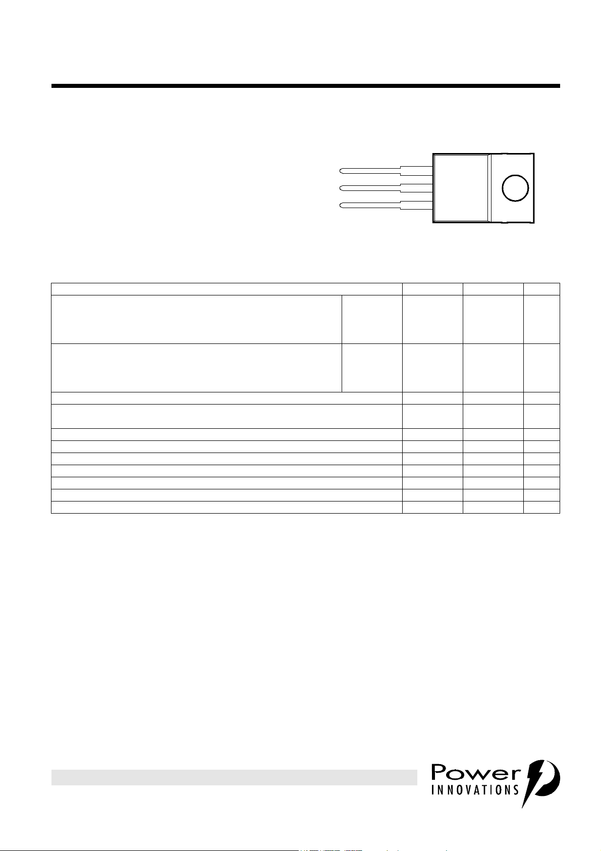
TO-220 PACKAGE
(TOP VIEW)
K
A
G
1
2
3
Pin 2 is in electrical contact with the mounting base.
absolute maximum ratings over operating case temperature (unless otherwise noted)
RATING SYMBOL VALUE UNIT
TIC116D
Repetitive peak off-state voltage
Repetitive peak reverse voltage
Continuous on-state current at (or below) 70°C case temperature (see Note 1) I
Average on-state current (180° conduction angle) at (or below) 70°C case temperature
(see Note 2)
Surge on-state current at (or below) 25°C case temperature (see Note 3) I
Peak positive gate current (pulse width
Peak gate power dissipation (pulse width
Average gate power dissipation (see Note 4) P
Operating case temperature range T
Storage temperature range T
Lead temperature 1.6 mm from case for 10 seconds T
NOTES: 1. These values apply for continuous dc operation with resistive load. Above 70°C derate linearly to zero at 110°C.
2. This value may be applied continuously under single phase 50 Hz half-sine-wave operation with resistive load. Above 70°C derate
linearly to zero at 110°C.
3. This value applies for one 50 Hz half-sine-wave when the device is operating at (or below) the rated value of peak reverse voltage
and on-state current. Surge may be repeated after the device has returned to original thermal equilibrium.
4. This value applies for a maximum averaging time of 20 ms.
≤ 300 µs) I
≤ 300 µs) P
TIC116M
TIC116S
TIC116N
TIC116D
TIC116M
TIC116S
TIC116N
V
DRM
V
RRM
T(RMS)
I
T(AV)
TM
GM
GM
G(AV)
C
stg
L
400
600
700
800
400
600
700
800
80 A
-40 to +110 °C
-40 to +125 °C
230 °C
MDC1ACA
V
V
8 A
5 A
3 A
5 W
1 W
PRODUCT INFORMATION
Information is current as of publication date. Products conform to specifications in accordance
with the terms of Power Innovations standard warranty. Production processing does not
necessarily include testing of all parameters.
1
Page 2
TIC116 SERIES
SILICON CONTROLLED RECTIFIERS
APRIL 1971 - REVISED JUNE 2000
electrical characteristics at 25°C case temperature (unless otherwise noted)
PARAMETER TEST CONDITIONS MIN TYP MAX UNIT
I
I
dv/dt
Repetitive peak
DRM
off-state current
Repetitive peak
RRM
reverse current
Gate trigger current VAA = 12 V R
I
GT
Gate trigger voltage
V
GT
Holding current
I
H
On-state
V
T
voltage
Critical rate of rise of
off-state voltage
NOTE 5: This parameter must be measured using pulse techniques, t
the current carrying contacts, are located within 3.2 mm from the device body.
= rated V
V
D
= rated V
V
R
V
= 12 V
AA
≥ 20 µs
t
p(g)
= 12 V
V
AA
≥ 20 µs
t
p(g)
= 12 V
V
AA
≥ 20 µs
t
p(g)
V
= 12 V
AA
Initiating I
= 12 V
V
AA
Initiating I
= 8 A (see Note 5) 1.7 V
I
T
= rated V
V
D
DRM
RRM
= 100 mA
T
= 100 mA
T
D
IG = 0 TC = 110°C 2 mA
= 100 Ω t
L
R
= 100 Ω T
L
R
= 100 Ω
L
R
= 100 Ω T
L
IG = 0 TC = 110°C 400 V/µs
= 300 µs, duty cycle ≤ 2 %. Voltage sensing-contacts, separate from
p
TC = 110°C 2 mA
≥ 20 µs 8 20 mA
p(g)
= - 40°C
C
= 110°C
C
T
= - 40°C
C
0.2
2.5
0.8 1.5
100
40
V
mA
thermal characteristics
R
R
Junction to case thermal resistance 3 °C/W
θJC
Junction to free air thermal resistance 62.5 °C/W
θJA
PARAMETER MIN TYP MAX UNIT
PRODUCT INFORMATION
2
Page 3
SILICON CONTROLLED RECTIFIERS
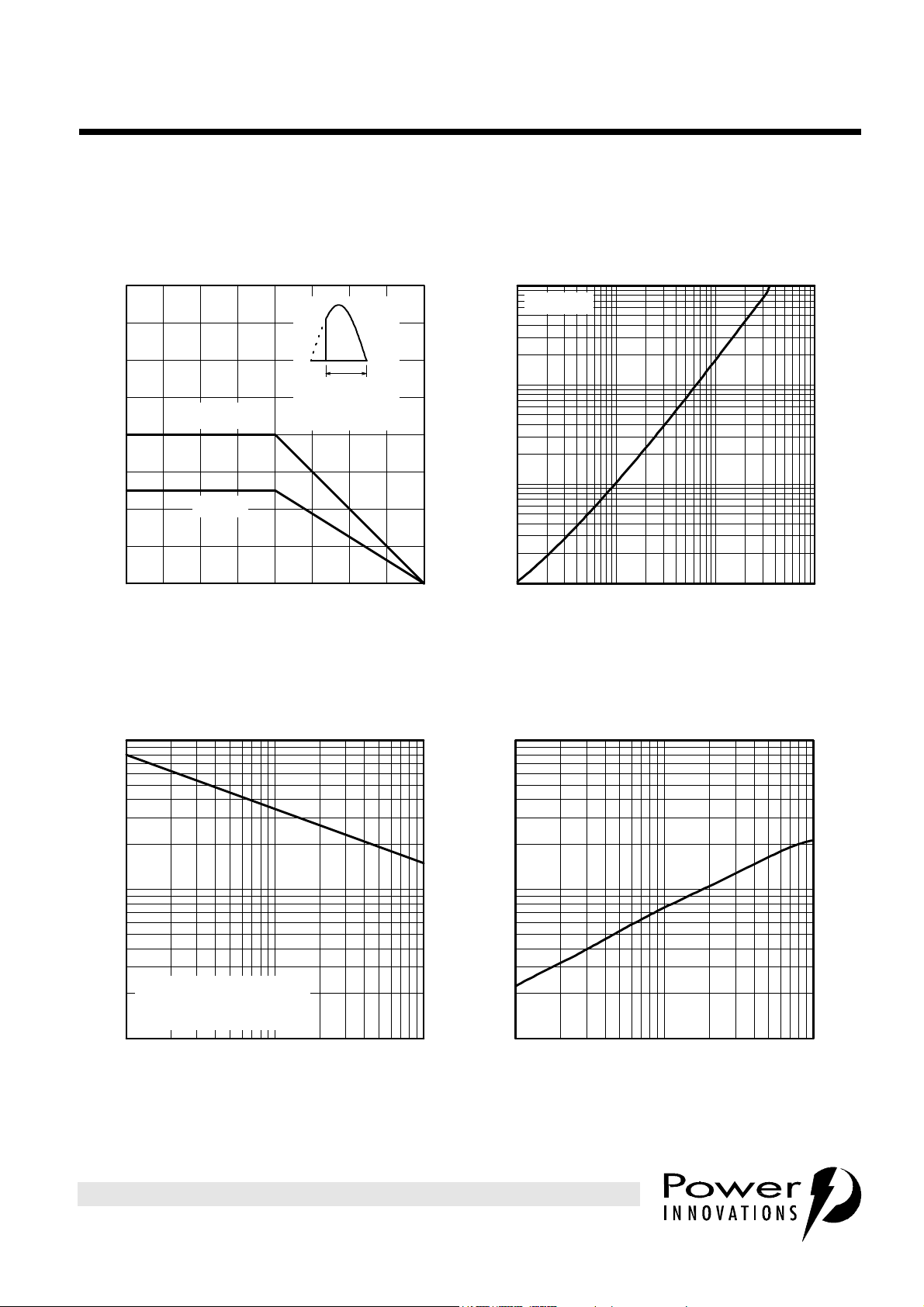
AVERAGE ON-STATE CURREN
T
MAX ANODE POWER LOSS
P
- Max Continuous Anode Power Dissipated- W
SURGE ON-STATE CURRENT
I
- Peak Half-Sine-Wave Current - A
TRANSIENT THERMAL RESISTANC
E
THERMAL INFORMATION
TIC116 SERIES
APRIL 1971 - REVISED JUNE 2000
DERATING CURVE
16
14
12
10
Continuous DC
8
6
4
- Maximum Average On-State Current - A
2
T(AV)
I
0
30 40 50 60 70 80 90 100 110
ΦΦ = 180°
TC - Case Temperature - °C
0° 180°
ΦΦ
Conduction
Angle
Figure 1. Figure 2.
TI03AA
vs
ON-STATE CURRENT
100
TJ = 110°C
10
1
A
0·1
0·1 1 10 100
IT - Continuous On-State Current - A
TI03AB
vs
CYCLES OF CURRENT DURATION
100
10
TM
T
≤≤ 70°C
C
No Prior Device Conduction
Gate Control Guaranteed
1
1 10 100
Consecutive 50 Hz Half-Sine-Wave Cycles
Figure 3. Figure 4.
TI03AC
vs
CYCLES OF CURRENT DURATION
10
1
- Transient Thermal Resistance - °C/W
θ
θJC(t)
R
0·1
1 10 100
Consecutive 50 Hz Half-Sine-Wave Cycles
TI03AD
PRODUCT INFORMATION
3
Page 4

TIC116 SERIES
GATE TRIGGER CURRENT
GATE TRIGGER VOLTAGE
HOLDING CURRENT
I
- Holding Current - mA
PEAK ON-STATE VOLTAGE
SILICON CONTROLLED RECTIFIERS
APRIL 1971 - REVISED JUNE 2000
TYPICAL CHARACTERISTICS
vs
CASE TEMPERATURE
VAA =12 V
R
= 100 ΩΩ
L
t
≥≥ 20 µs
p(g)
10
- Gate Trigger Current - mA
GT
I
1
-50 -25 0 25 50 75 100 125
TC - Case Temperature - °C
Figure 5. Figure 6.
TC03AA
vs
CASE TEMPERATURE
1
0·8
0·6
0·4
- Gate Trigger Voltage - V
GT
V
0·2
VAA =12 V
R
= 100 ΩΩ
L
t
≥≥ 20 µs
p(g)
0
-50 -25 0 25 50 75 100 125
TC - Case Temperature - °C
TC03AB
vs
CASE TEMPERATURE
100
VAA = 12 V
Initiating IT = 100 mA
10
H
1
-50 -25 0 25 50 75 100 125
TC - Case Temperature - °C
Figure 7. Figure 8.
TC03AD
vs
PEAK ON-STATE CURRENT
2·5
TC = 25 °C
tP = 300 µs
Duty Cycle ≤≤ 2 %
2
1·5
1
- Peak On-State Voltage - V
TM
V
0·5
0
0·1 1 10 100
ITM - Peak On-State Current - A
TC03AE
PRODUCT INFORMATION
4
Page 5

TIC116 SERIES
NOTE A: The centre pin is in electrical contact with the mounting tab.
SILICON CONTROLLED RECTIFIERS
APRIL 1971 - REVISED JUNE 2000
MECHANICAL DATA
TO-220
3-pin plastic flange-mount package
This single-in-line package consists of a circuit mounted on a lead frame and encapsulated within a plastic
compound. The compound will withstand soldering temperature with no deformation, and circuit performance
characteristics will remain stable when operated in high humidity conditions. Leads require no additional
cleaning or processing when used in soldered assembly.
TO-220
3,96
ø
3,71
18,0 TYP.
0,97
0,66
10,4
10,0
1 2 3
1,47
1,07
2,74
2,34
5,28
4,68
2,95
2,54
6,1
5,6
4,70
4,20
1,32
1,23
6,6
6,0
15,32
14,55
14,1
12,7
0,64
0,41
2,90
2,40
ALL LINEAR DIMENSIONS IN MILLIMETERS
PRODUCT INFORMATION
5
Page 6

TIC116 SERIES
SILICON CONTROLLED RECTIFIERS
APRIL 1971 - REVISED JUNE 2000
IMPORTANT NOTICE
Power Innovations Limited (PI) reserves the right to make changes to its products or to discontinue any
semiconductor product or service without notice, and advises its customers to verify, before placing orders, that the
information being relied on is current.
PI warrants performance of its semiconductor products to the specifications applicable at the time of sale in
accordance with PI's standard warranty. Testing and other quality control techniques are utilized to the extent PI
deems necessary to support this warranty. Specific testing of all parameters of each device is not necessarily
performed, except as mandated by government requirements.
PI accepts no liability for applications assistance, customer product design, software performance, or infringement
of patents or services described herein. Nor is any license, either express or implied, granted under any patent
right, copyright, design right, or other intellectual property right of PI covering or relating to any combination,
machine, or process in which such semiconductor products or services might be or are used.
PI SEMICONDUCTOR PRODUCTS ARE NOT DESIGNED, INTENDED, AUTHORIZED, OR WARRANTED TO BE
SUITABLE FOR USE IN LIFE-SUPPORT APPLICATIONS, DEVICES OR SYSTEMS.
Copyright © 2000, Power Innovations Limited
PRODUCT INFORMATION
6
 Loading...