

Page 1
ABOUT THIS DEVICE
Samsung's latest 58nm 1Gbit DDR3 SDRAM
(K4B1G0846E) features the most advanced
Samsung DDR3 SDRAM product Semiconductor
Insights (SI) has analyzed to date. This device has a
58nm process node and boasts 1Gbit of memory with
impressive die area efficiency of 24Mbits per mm .
2
Samsung made significant improvements to their
DRAM technology over the past several process
generations. At the 80nm process node they have
adopted 6F2 cell technology. This time around one of
the outstanding changes is the reduction of metal
layer. With only three layers of metal interconnect,
this 58nm 1Gbit DRAM achieves the highest Mbits
per mm efficiency seen in any 1Gbit DDR3 SDRAM
2
product.
Semiconductor Insights is currently analyzing major
circuit blocks of this device to better understand the
manufacturer's move in developing this DDR3
product.
Semiconductor Insights' in depth analysis of the
58nm DRAM circuit analysis combined with already
finished process technology analysis on the 58nm
1Gbit DDR2 SDRAM will help shed light on the
different choices, optimization and trade-offs
Samsung has made to maintain its leadership in the
DRAM market.
Source: Semiconductor Insights, 2009
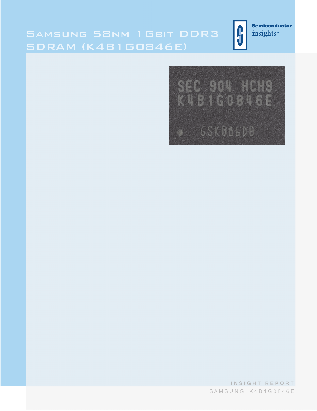
Package Photograph of the Samsung 58nm DDR3 SDRAM
DEVICE HIGHLIGHTS
The following details were taken from the
manufacturer's product information.
?Adoption of the latest 58nm DRAM process
technology JEDEC standard VDD = 1.5V Power
Supply
?VDDQ = 1.5V
?DQ shielding, self calibration and fly-by topology
for better signal control
?Bidirectional DQS (differential default)
?BL = 4, 8 (8 bits prefetch)
?8 banks architecture
?External RESET pin
Semiconductor Insights expects that the 58nm 1Gbit
DDR3 SDRAM will be Samsung's main product in the
growing DDR3 market in 2009 and beyond.
APPLICATION
The application areas for the 1Gbit DDR3 SDRAMs
include PC's such as laptops, servers, and other
consumer electronics.
COMPETING NAND VENDORS
Hynix, Micron, Elpida
S E M I C O N D U C T O R I N S I G H T S
Page 2
Source: Semiconductor Insights, 2009 Source: Semiconductor Insights, 2009
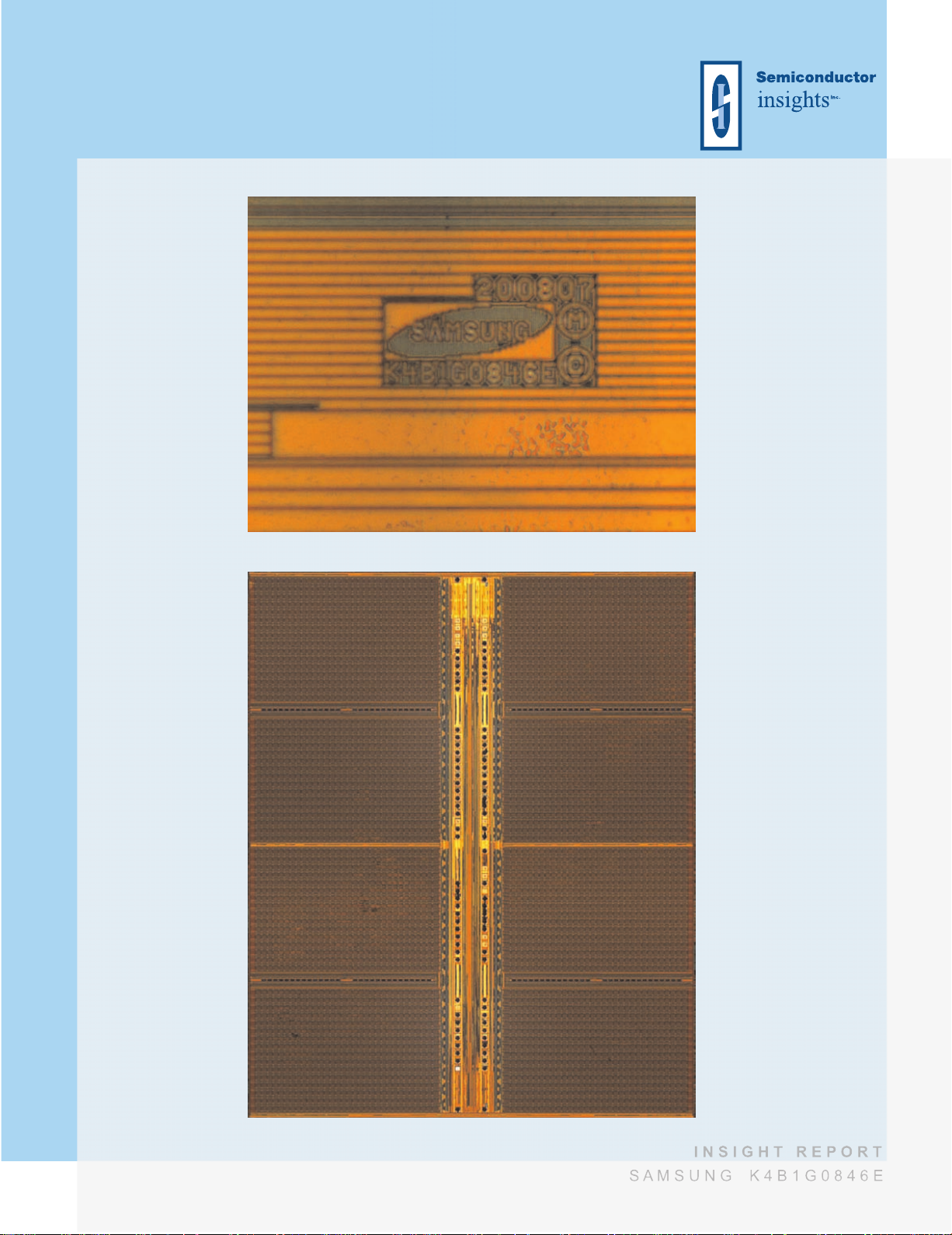
Die Markings of the Samsung 58nm DDR3 SDRAM
S E M I C O N D U C T O R I N S I G H T S
Die Photograph of the Samsung 58nm DDR3 SDRAM
 Loading...