

Page 1

ABOUT THIS DEVICE
Samsung's latest Multi-Level Cell (MLC) NAND
Flash features an advanced floating gate 42nm
NAND Flash process. To date, this is the most
advanced NAND Flash process Semiconductor
Insights (SI) has analyzed by this manufacturer.
This latest product features 16Gbit of non-volatile
memory storage and has a chip size of 114mm2, a
30% reduction from the previous 51nm 16Gbit MLC
NAND Flash product (K9GAG08U0M).
The new architecture looks slightly different from the
previous generation. Samsung has placed all the
pads on one edge of the die and there is only one row
decoder strip located in the centre of the die. The
previous node had two row decoder strips effectively
reducing wordline length. Initial analysis of the
Samsung K9GAG08U0D revealed some notable
process improvements including use of new
interconnect material, which might help explain the
architectural choices that the manufacturer made
with this device. It also appears that Samsung has
implemented very interesting measures to achieve
reliable operations at this advanced geometry.
APPLICATION
Samsung provides a very small form factor solution
for high density, solid-state storage. Samsung's
NAND Flash memory products are optimized for
general solid-state storage, image file storage and
audio for applications such as MP3 players, solidstate drives, digital cameras, audio appliances, settop boxes and industrial storage.
COMPETING NAND VENDORS
Source: Semiconductor Insights, 2008
Package Photograph of the Samsung 42nm 16 Gbit
NAND Flash
DEVICE HIGHLIGHTS
Voltage supply:
?
?2.7V device: 2.5V ~ 2.9V
?3.3V device: 2.7V ~ 3.6V
?Organization: 2G x 8bit
?Automatic Program and Erase
?Page Read Operation
?Memory Cell: 2bit / Memory Cell
?Command/Address/Data Multiplexed I/O Port
?Hardware Data Protection
?Reliable CMOS Floating Gate Technology
?Command Register Operation
Toshiba, IM Flash Technologies, Hynix, Numonyx
S E M I C O N D U C T O R I N S I G H T S
Page 2
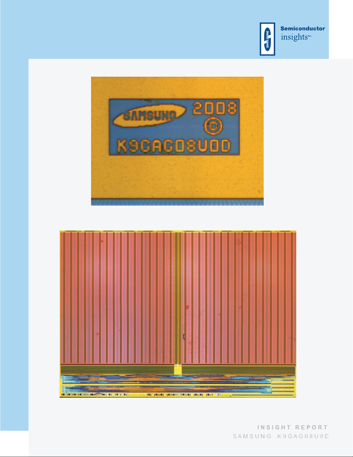
Source: Semiconductor Insights, 2008
Die Markings of the Samsung 42nm 16 Gbit NAND Flash
Source: Semiconductor Insights, 2008
Die Photograph of the Samsung 42nm 16 Gbit NAND Flash
S E M I C O N D U C T O R I N S I G H T S
 Loading...