

Datasheet THS6022IPWPR, THS6022IPWP, THS6022EVM, THS6022CPWPR, THS6022CPWP Datasheet (Texas Instruments)
Page 1
THS6022
250-mA DUAL DIFFERENTIAL LINE DRIVER
SLOS225C – SEPTEMBER 1998 – REVISED JANUARY 2000
1
POST OFFICE BOX 655303 • DALLAS, TEXAS 75265
D
ADSL, HDSL and VDSL Diff. Line Driver
D
200 mA Output Current Minimum Into 50-Ω
Load
D
High Speed
– 210 MHz Bandwidth (–3dB) at 50-Ω Load
– 300 MHz Bandwidth (–3dB) at 100-Ω Load
– 1900 V/µs Slew Rate, G = 5
D
Low Distortion
– –69 dB 3rd Order Harmonic Distortion at
f = 1 MHz, 50-Ω Load, and V
O(PP)
= 20 V
D
Independent Power Supplies for Low
Crosstalk
D
Wide Supply Range ±5 V to ±15 V
D
Thermal Shutdown and Short Circuit
Protection
D
Evaluation Module Available
description
The THS6022 contains two high-speed drivers
capable of providing 200 mA output current (min)
into a 50-Ω load. These drivers can be configured
differentially to drive a 50-V p-p output signal over
low-impedance lines. The drivers are current
feedback amplifiers, designed for the high slew
rates necessary to support low total harmonic
distortion (THD) in xDSL applications. The
THS6022 is ideally suited for asymmetrical digital
subscriber line (ADSL) at the remote terminal, high data rate digital suscriber line (HDSL), and very high data
rate digital suscriber line (VDSL), where it supports the high-peak voltage and current requirements of these
applications. Separate power supply connections for each driver are provided to minimize crosstalk.
HIGH-SPEED xDSL LINE DRIVER/RECEIVER FAMILY
DEVICE
DRIVER RECEIVER DESCRIPTION
THS6002
•
• Dual differential line drivers and receivers
THS6012 • 500-mA dual differential line driver
THS6022 • 250-mA dual differential line driver
THS6032 • Low-power ADSL central office line driver
THS6062 • Low-noise ADSL receiver
THS7002 • Low-noise programmable gain ADSL receiver
CAUTION: The THS6022 provides ESD protection circuitry. However, permanent damage can still occur if this device is subjected
to high-energy electrostatic discharges. Proper ESD precautions are recommended to avoid any performance degradation or loss
of functionality.
Copyright 2000, Texas Instruments Incorporated
PRODUCTION DATA information is current as of publication date.
Products conform to specifications per the terms of Texas Instruments
standard warranty. Production processing does not necessarily include
testing of all parameters.
Please be aware that an important notice concerning availability, standard warranty, and use in critical applications of
Texas Instruments semiconductor products and disclaimers thereto appears at the end of this data sheet.
PowerPAD is a trademark of Texas Instruments Incorporated.
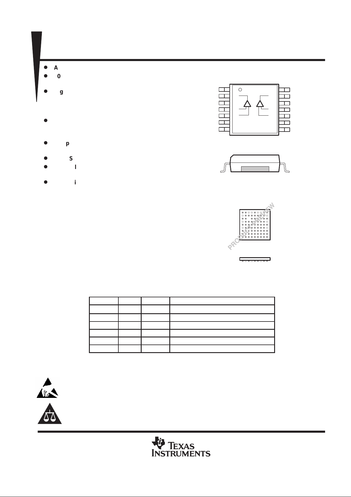
Cross Section View Showing PowerPAD
NC – No internal connection
VCC–
1OUT
V
CC+
1IN+
1IN–
NC
NC
V
CC
–
2OUT
V
CC+
2IN+
2IN–
NC
NC
1
2
3
4
5
6
7
14
13
12
11
10
9
8
Thermally Enchanced TSSOP (PWP)
PowerPAD Package
(TOP VIEW)
†
This terminal is internally connected to the thermal pad.
(SIDE VIEW)
(SIDE VIEW)
MicroStar Junior (GQE) Package
(TOP VIEW)
Page 2
THS6022
250-mA DUAL DIFFERENTIAL LINE DRIVER
SLOS225C – SEPTEMBER 1998 – REVISED JANUARY 2000
2
POST OFFICE BOX 655303 • DALLAS, TEXAS 75265
description (continued)
The THS6022 is packaged in the patented PowerPAD package. This package provides outstanding thermal
characteristics in a small footprint package, which is fully compatible with automated surface-mount assembly
procedures. The exposed thermal pad on the underside of the package is in direct contact with the die. By simply
soldering the pad to the PWB copper and using other thermal outlets, the heat is conducted away from the
junction.
AVAILABLE OPTIONS
PACKAGED DEVICE
T
A
PowerPAD PLASTIC
SMALL OUTLINE
†
(PWP)
MicroStar Junior
(GQE)
EVALUATION
MODULE
0°C to 70°C THS6022CPWP THS6022CGQE THS6022EVM
–40°C to 85°C THS6022IPWP THS6022IGQE —
†
The PWP packages are available taped and reeled. Add an R suffix to the device type (i.e.,
THS6022CPWPR)
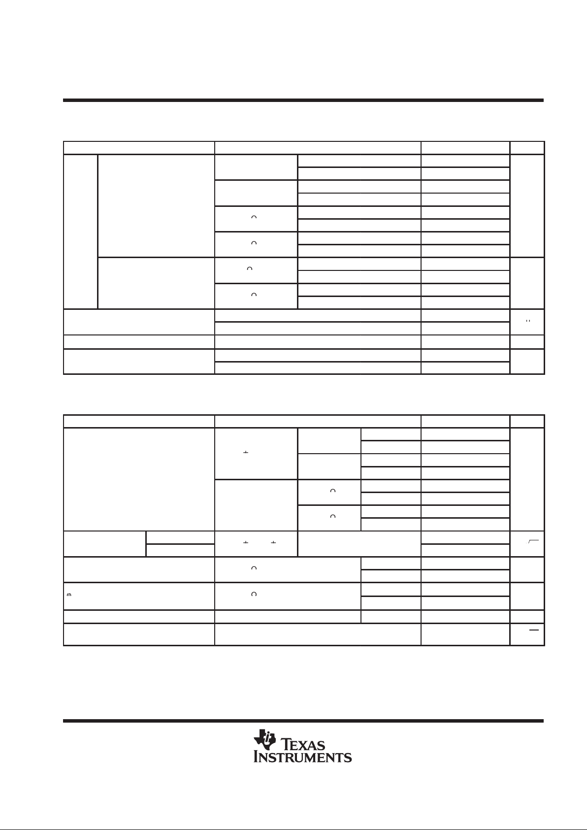
Terminal Functions
TERMINAL
NAME PWP PACKAGE
TERMINAL NO.
GQE PACKAGE
TERMINAL NO.
1OUT 2 A3
1IN– 5 F1
1IN+ 4 D1
2OUT 13 A7
2IN– 10 F9
2IN+ 11 D9
V
CC+
3, 12 B1, B9
V
CC–
1, 14 A4, A6
NC 6, 7, 8 ,9 NA
Page 3
THS6022
250-mA DUAL DIFFERENTIAL LINE DRIVER
SLOS225C – SEPTEMBER 1998 – REVISED JANUARY 2000
3
POST OFFICE BOX 655303 • DALLAS, TEXAS 75265
pin assignments
98765
A
B
C
D
E
F
321
G
H
J
4
2IN+
1N+
1IN–
NC
NC
NC
NC
NC
NCNC NC NC NC
NC NC NC
NC NC NC
NC NC NC
NC NC
NC NC NC
V
CC+
NCNC
NCNC
NC
NC
NCNC NC
NCNC NC
NC NC
NC NC
NC
NC
NC
NC
NC NC
NC
2OUT
NC
NC
NC NCNC NC
NC
NC NC NC
NC
NC
1OUT
NC NC
2IN–
NC
NCNC
NC
V
CC+
NOTE: Shaded terminals are used for thermal connection to the ground plane.
MicroStarJunior (GQE) Package
(TOP VIEW)
V
CC–
V
CC–
NC
NCNCNC
NC
Page 4
THS6022
250-mA DUAL DIFFERENTIAL LINE DRIVER
SLOS225C – SEPTEMBER 1998 – REVISED JANUARY 2000
4
POST OFFICE BOX 655303 • DALLAS, TEXAS 75265
functional block diagram
_
+
Driver 1
Driver 2
_
+
3
4
5
11
10
2
1
12
13
14
VCC+
V
CC+
V
CC–
VCC–
1OUT
2 OUT
1 IN+
1 IN–
2 IN+
2 IN–
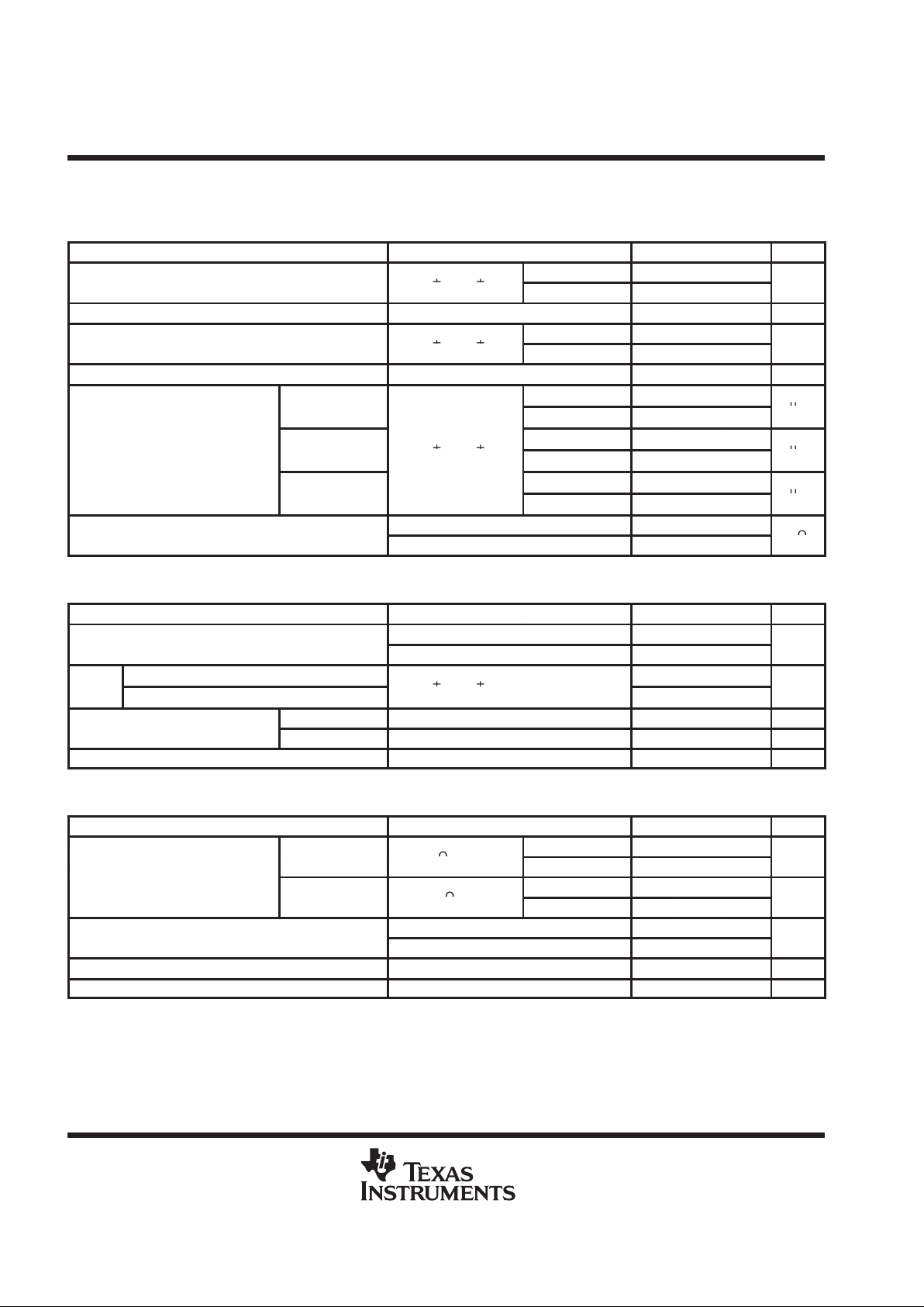
absolute maximum ratings over operating free-air temperature (unless otherwise noted)
†
Supply voltage, V
CC+
to V
CC–
33 V. . . . . . . . . . . . . . . . . . . . . . . . . . . . . . . . . . . . . . . . . . . . . . . . . . . . . . . . . . . . . . .
Input voltage, VI ±V
CC
. . . . . . . . . . . . . . . . . . . . . . . . . . . . . . . . . . . . . . . . . . . . . . . . . . . . . . . . . . . . . . . . . . . . . . . . . .
Output current, IO (see Note 1) 400 mA. . . . . . . . . . . . . . . . . . . . . . . . . . . . . . . . . . . . . . . . . . . . . . . . . . . . . . . . . . . .
Differential input voltage, V
ID
6 V. . . . . . . . . . . . . . . . . . . . . . . . . . . . . . . . . . . . . . . . . . . . . . . . . . . . . . . . . . . . . . . . .
Continuous total power dissipation at (or below) TA = 25°C (see Note 1) 3.3 W. . . . . . . . . . . . . . . . . . . . . . . . . .
Operating free air temperature, T
A
–40°C to 85°C. . . . . . . . . . . . . . . . . . . . . . . . . . . . . . . . . . . . . . . . . . . . . . . . . . .
Storage temperature, T
stg
–65°C to 125°C. . . . . . . . . . . . . . . . . . . . . . . . . . . . . . . . . . . . . . . . . . . . . . . . . . . . . . . . .
Lead temperature, 1,6 mm (1/16 inch) from case for 10 seconds 300°C. . . . . . . . . . . . . . . . . . . . . . . . . . . . . . .
†
Stresses beyond those listed under “absolute maximum ratings” may cause permanent damage to the device. These are stress ratings only, and
functional operation of the device at these or any other conditions beyond those indicated under “recommended operating conditions” is not
implied. Exposure to absolute-maximum-rated conditions for extended periods may affect device reliability.
NOTE 1: The THS6022 incorporates a PowerPad on the underside of the chip. This acts as a heatsink and must be connected to a thermal
dissipation plane for proper power dissipation. Failure to do so can result in exceeding the maximum junction temperature, which could
permanently damage the device. See the
Thermal Information
section of this document for more information about PowerPad
technology.
recommended operating conditions
MIN NOM MAX UNIT
pp
Split supply ±4.5 ±16
Suppl
y v
oltage, V
CC+
and V
CC–
Single supply 9 32
V
p
p
C Suffix 0 70
°
O erating free-air tem erature, T
A
I Suffix –40 85
°C
Page 5
THS6022
250-mA DUAL DIFFERENTIAL LINE DRIVER
SLOS225C – SEPTEMBER 1998 – REVISED JANUARY 2000
5
POST OFFICE BOX 655303 • DALLAS, TEXAS 75265
electrical characteristics, VCC = ±15 V, RL = 50 Ω, RF = 1 kΩ, TA = 25°C (unless otherwise noted)
dynamic performance
PARAMETER TEST CONDITIONS MIN TYP MAX UNIT
VCC = ±15 V RF = 787 Ω 210
V
O
=
200 mV
, G =
1
VCC = ±5 V RF = 910 Ω 150
VCC = ±15 V RF = 590 Ω 200
V
O
=
200 mV
, G =
2
VCC = ±5 V RF = 715 Ω 140
Small-signal bandwidth (–3 dB)
VCC = ±15 V RF = 750 Ω 300
MH
z
R
L
=
100 Ω
, G =
1
VCC = ±5 V RF = 910 Ω 210
BW
VCC = ±15 V RF = 620 Ω 260
R
L
=
100 Ω
, G =
2
VCC = ±5 V RF = 680 Ω 180
VCC = ±15 V RF = 590 Ω 115
R
L
= 50 Ω, G = 2,
VCC = ±5 V RF = 715 Ω 70
Bandwidth for 0.1 dB flatness
VCC = ±15 V RF = 620 Ω 140
MH
z
R
L
=
100 Ω
, G = 2,
VCC = ±5 V RF = 680 Ω 80
VCC = ±15 V, V
O(PP)
= 20 V, G = 5 1900
SR
Slew rate (see Note 2)
VCC = ±5 V, V
O(PP)
= 5 V, G = 2 950
V/µs
t
s
Settling time to 0.1% 0 V to 10 V Step, G = 2, RL = 1 kΩ 70 ns
Full power bandwidth
VCC = ±15 V, VO = 20 V
(PP)
30
(see Note 3)
VCC = ±5 V, VO = 4 V
(PP)
75
MH
z
NOTES: 2. Slew rate is measured from an output level range of 25% to 75%.
3. Full power bandwidth = slew rate/2πV
peak
noise/distortion performance
PARAMETER TEST CONDITIONS MIN TYP MAX UNIT
V
O(PP)
= 20 V –69
f
=
500 kH
z
V
O(PP)
= 2 V –80
V
CC
=
±15 V
, G =
2
V
O(PP)
= 20 V –66
f
= 1 MHz
V
O(PP)
= 2 V –75
THD
Total harmonic distortion
f = 500 kHz –71
dBc
V
= ±5 V,
R
L
=
25 Ω
f = 1 MHz –65
CC
,
V
O(PP)
= 2 V, G = 2
f = 500 kHz –78
R
L
=
50 Ω
f = 1 MHz –72
Input noise
Positive (IN+)
11.5
I
n
current
Negative (IN–)
V
CC
= ±5 V or
±15 V
,
G
= 2,
f
= 10 kHz,
16
p
A/√H
z
NTSC,
VCC = ±5 V 0.03%
ADDifferential gain error
R
L
=
150 Ω
, G =
2
,
40 IRE Mod.
VCC = ±15 V
0.04%
p
NTSC,
VCC = ±5 V 0.08°
φDDifferential hase error
R
L
=
150 Ω
, G =
2
40 IRE Mod.
VCC = ±15 V
0.06°
Crosstalk VI = 200 mV , f = 1 MHz –64 dB
V
n
Input voltage noise
VCC = ±5 V or ±15 V,
Single-ended
f = 10 kHz, G = 2,
1.7 nV/√Hz
Page 6
THS6022
250-mA DUAL DIFFERENTIAL LINE DRIVER
SLOS225C – SEPTEMBER 1998 – REVISED JANUARY 2000
6
POST OFFICE BOX 655303 • DALLAS, TEXAS 75265
electrical characteristics, VCC = ±15 V, RL = 50 Ω, RF = 1 kΩ, TA = 25°C (unless otherwise noted)
(continued)
dc performance
PARAMETER TEST CONDITIONS
†
MIN TYP MAX UNIT
p
TA = 25°C 1 5
VIOInput offset voltage
V
CC
=
±5 V or ±15 V
TA = full range 7
mV
Input offset voltage drift VCC = ±5 V or ±15 V, TA = full range 20 µV/°C
p
TA = 25°C 0.5 4
Differential input offset voltage
V
CC
= ±5 V or
±15 V
TA = full range 5
mV
Differential input offset voltage drift VCC = ±5 V or ±15 V, TA = full range 10 µV/°C
TA = 25°C 1 9
Negative
TA = full range 12
µA
p
TA = 25°C 5 10
IIBIn ut bias current
Positive
V
CC
= ±5 V or
±15 V
TA = full range 12
µA
TA = 25°C 1.5 8
Differential
TA = full range 11
µA
p
p
VCC = ±5 V 1
Open loop transresistance
VCC = ±15 V 4
MΩ
†
Full range is 0°C to 70°C for the THS6022C and –40°C to 85°C for the THS6022I.
input characteristics
PARAMETER TEST CONDITIONS
†
MIN TYP MAX UNIT
p
VCC = ±5 V ±3.5 ±3.6
V
ICR
Common-mode input voltage range
VCC = ±15 V ±13.3 ±13.4
V
Common-mode rejection ratio
62 73
CMRR
Differential common-mode rejection ratio
V
CC
= ±5 V or
±15 V
,
T
A
=
full range
100
dB
p
+ Input 1.5 MΩ
riInput resistance
– Input 15 Ω
C
i
Input capacitance 1.4 pF
†
Full range is 0°C to 70°C for the THS6022C and –40°C to 85°C for the THS6022I.
output characteristics
PARAMETER TEST CONDITIONS
†
MIN TYP MAX UNIT
VCC = ±5 V ±3.1 ±3.2
p
Single ended
R
L
= 50
Ω
VCC = ±15 V ±12.3 ±12.6
V
VOOutput voltage swing
VCC = ±5 V ±6.2 ±6.6
Differential
R
L
=
100 Ω
VCC = ±15 V ±24.6 ±25.2
V
p
VCC = ±5 V, RL = 5 Ω 250
IOOutput current (see Note 2)
VCC = ±15 V, RL = 50 Ω 200 250
mA
I
OS
Short-circuit output current (see Note 4) 400 mA
R
O
Output resistance Open loop 13 Ω
†
Full range is 0°C to 70°C for the THS6022C and –40°C to 85°C for the THS6022I.
NOTES: 2. Slew rate is measured from an output level range of 25% to 75%.
4. A heat sink is required to keep the junction temperature below absolute maximum when an output is heavily loaded or shorted. See
absolute maximum ratings and Thermal Information section.
Page 7
THS6022
250-mA DUAL DIFFERENTIAL LINE DRIVER
SLOS225C – SEPTEMBER 1998 – REVISED JANUARY 2000
7
POST OFFICE BOX 655303 • DALLAS, TEXAS 75265
electrical characteristics, VCC = ±15 V, RL = 50 Ω, RF = 1 kΩ, TA = 25°C (unless otherwise noted)
(continued)
power supply
PARAMETER TEST CONDITIONS
†
MIN TYP MAX UNIT
pp
p
Split supply ±4.5 ±16.5
VCCPower supply operating range
Single supply 9 33
V
TA = 25°C 6 8
V
CC
= ±5
V
TA = full range 10
ICCQuiescent current (each driver)
TA = 25°C 7.2 9
mA
V
CC
=
±15 V
TA = full range 11
TA = 25°C –68 –76
pp
V
CC
=
±5 V
TA = full range –65
dB
PSRR
Power supply rejection ratio
TA = 25°C –64 –75
V
CC
=
±15 V
TA = full range –62
dB
†
Full range is 0°C to 70°C for the THS6022C and –40°C to 85°C for the THS6022I.
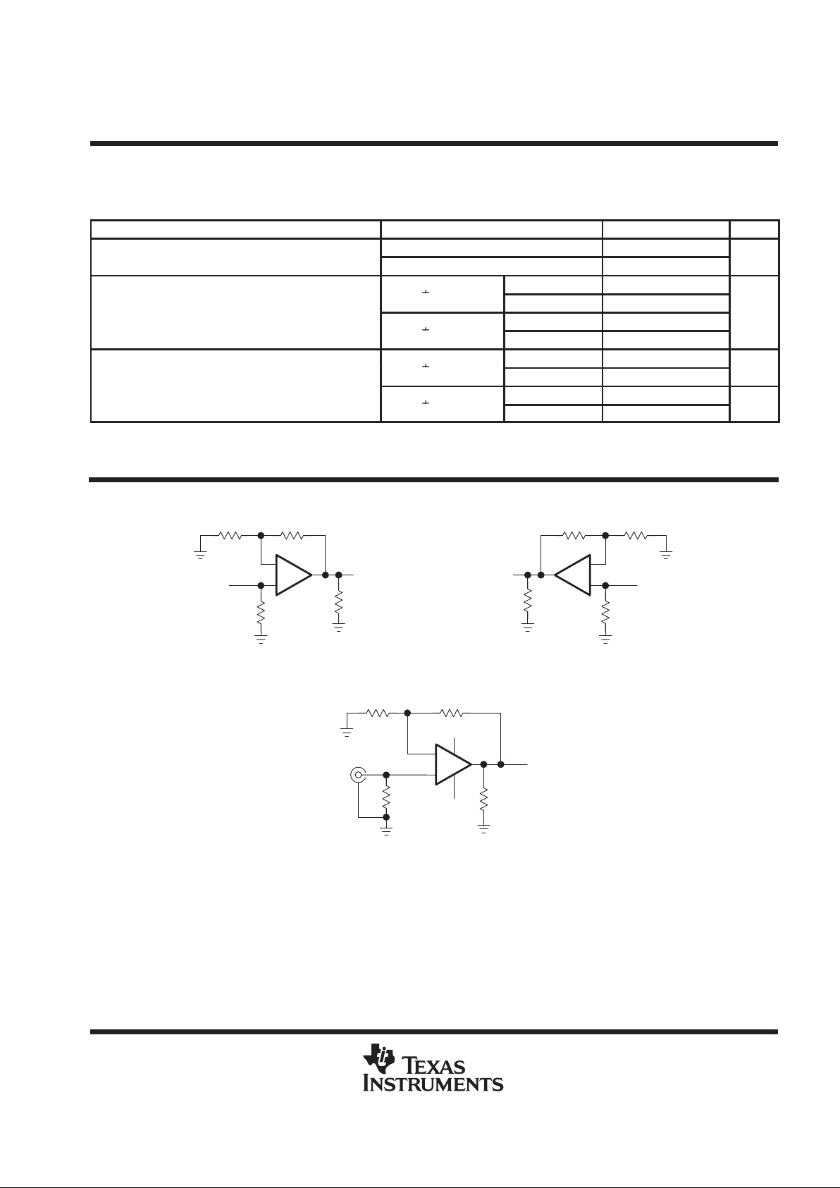
PARAMETER MEASUREMENT INFORMATION
+
–
1 kΩ
V
I
V
O
50 Ω
50 Ω
1 kΩ
Driver 1
+
–
1 kΩ
V
I
V
O
50 Ω
50 Ω
1 kΩ
Driver 2
Figure 1. Input-to-Output Crosstalk Test Circuit
V
I
V
O
+
–
R
G
R
F
R
L
50 Ω
50 Ω
V
CC–
V
CC+
Figure 2. Test Circuit, Gain = 1 + (RF/RG)
Page 8
THS6022
250-mA DUAL DIFFERENTIAL LINE DRIVER
SLOS225C – SEPTEMBER 1998 – REVISED JANUARY 2000
8
POST OFFICE BOX 655303 • DALLAS, TEXAS 75265
TYPICAL CHARACTERISTICS
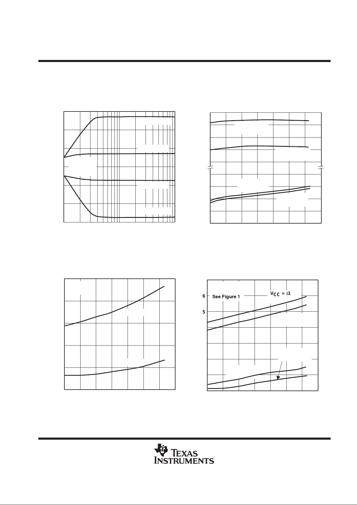
Table of Graphs
FIGURE
V
O(PP)
Peak-to-peak output voltage vs Load resistance 3
Maximum peak-to-peak output voltage swing vs Free-air temperature 4
V
IO
Input offset voltage vs Free-air temperature 5
I
IB
Input bias current vs Free-air temperature 6
Positive input bias current vs Common-mode input votlage 7
CMMR Common-mode rejection ratio vs Free-air temperature 8
Input-to-output crosstalk vs Frequency 9
PSSR Power supply rejection ratio vs Free-air temperature 10
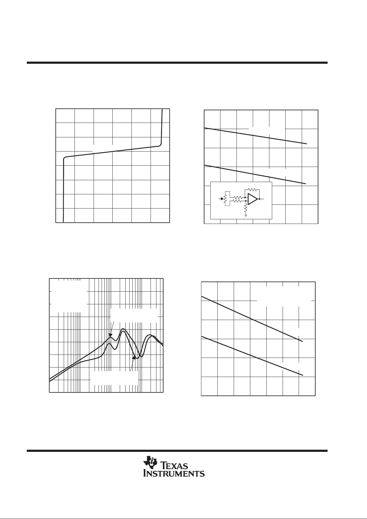
Closed-loop output impedance vs Frequency 11
I
CC
Supply current vs Free-air temperature 12
SR Slew rate vs Output step 13, 14
V
n
Input voltage noise vs Frequency 15
I
n
Input current noise vs Frequency 15
Output amplitude vs Frequency
16, 17,
19 – 32
Closed-loop output phase vs Frequency 18
Small and large frequency response 33 – 36
Single-ended output distortion vs Output voltage 37, 38
Harmonic distortion vs Frequency 39, 40
Differential gain Number of 150-Ω loads 41, 42
Differential phase Number of 150-Ω loads 43, 44
400-mV output step response 45, 47
20-V step response 46
4-V step response 48
Page 9
THS6022
250-mA DUAL DIFFERENTIAL LINE DRIVER
SLOS225C – SEPTEMBER 1998 – REVISED JANUARY 2000
9
POST OFFICE BOX 655303 • DALLAS, TEXAS 75265
TYPICAL CHARACTERISTICS
Figure 3
10 100 1 k
RL – Load Resistance – Ω
15
5
–5
–15
10
0
–10
VCC = ±15 V
VCC = ±5 V
PEAK-TO-PEAK OUTPUT VOLTAGE
vs
LOAD RESISTANCE
TA = 25°C
RF = 1 kΩ
Gain = 1
VCC = ±5 V
VCC = ±15 V
V
O(PP)
– Peak-to-Peak Output Voltage – V
Figure 4
TA – Free-Air Temperature – °C
–40 –20 0 20 80 1006040
4
3
2
3.5
2.5
14
13.5
12.5
13
12
VCC = ±15 V
50 Ω Load
VCC = ±5 V
No Load
VCC = ±5 V
50 Ω Load
VCC = ±15 V
No Load
| Maximum Peak-T o-Peak Output Voltage Swing | – V
MAXIMUM PEAK–TO-PEAK
OUTPUT VOLTAGE SWING
vs
FREE-AIR TEMPERATURE
Figure 5
TA – Free-Air Temperature – °C
–40 –20 0 20 80 1006040
VCC = ±5 V
INPUT OFFSET VOLTAGE
vs
FREE-AIR TEMPERATURE
VCC = ±15 V
V
IO
– Input Offset Voltage – mV
0.8
0.4
0
0.6
0.2
1
Gain = 1
RF = 1 kΩ
Figure 6
TA – Free-Air Temperature – °C
–40 –20 0 20 80 1006040
INPUT BIAS CURRENT
vs
FREE-AIR TEMPERATURE
7
3
1
0
4
2
I
IB
– Input Bias Current – Aµ
Gain = 1
RF = 1 kΩ
See Figure 1
5
6
VCC = ±15 V
I
IB+
VCC = ±5 V
I
IB+
VCC = ±15 V
I
IB–
VCC = ±5 V
I
IB–
Page 10
THS6022
250-mA DUAL DIFFERENTIAL LINE DRIVER
SLOS225C – SEPTEMBER 1998 – REVISED JANUARY 2000
10
POST OFFICE BOX 655303 • DALLAS, TEXAS 75265
TYPICAL CHARACTERISTICS
Figure 7
VIC – Common-Mode Input Voltage – V
POSITIVE INPUT BIAS CURRENT
vs
COMMON-MODE INPUT VOLTAGE
–5
–10
–15
–20
–10 0–5 5 15
20
–15
10
0
5
±15 V
10
15
I
IB+
– Input Bias Current – Aµ
Figure 8
TA – Free-Air Temperature – °C
CMRR – Common-Mode Rejection Ratio – dB
–40 –20 0 20 806040
75
65
60
90
70
VCC = ±5 V
COMMON-MODE REJECTION RATIO
vs
FREE-AIR TEMPERATURE
1 kΩ
1 kΩ
V
I
+
–
V
O
1 kΩ
1 kΩ
100
85
80
VCC = ±15 V
Figure 9
–90
100 k
–80
INPUT-TO-OUTPUT CROSSTALK
vs
FREQUENCY
0
500 M
f – Frequency – Hz
–40
–20
–10
–70
–60
1 M 10 M 100 M
–30
–50
Input-To-Output Crosstalk – dB
VCC = ±15 V
Gain = 2
RL = 50 Ω
RF = 1 kΩ
VO = 0.2 V
Driver 1 = Output
Driver 2 = Input
Driver 1 = Input
Driver 2 = Output
Figure 10
TA – Free-Air Temperature – °C
PSRR – Power Supply Rejection Ratio – dB
–40 –20 0 20 80 1006040
POWER SUPPLY REJECTION RATIO
vs
FREE-AIR TEMPERATURE
82
78
74
72
80
76
84
VCC+
VCC–
VCC = ±15 V or ±5 V
Gain = 1
RF = 1 kΩ
Page 11
THS6022
250-mA DUAL DIFFERENTIAL LINE DRIVER
SLOS225C – SEPTEMBER 1998 – REVISED JANUARY 2000
11
POST OFFICE BOX 655303 • DALLAS, TEXAS 75265
TYPICAL CHARACTERISTICS
Figure 11
0.01
100 k
100
500 M
f – Frequency – Hz
1
10
1 M 10 M 100 M
0.1
CLOSED-LOOP OUTPUT IMPEDANCE
vs
FREQUENCY
Gain = 2
RF = 1 kΩ
V
I(PP)
= 2 V
– Output Impedance –Z
o
Ω
VCC = ±5 V
VCC = ±15 V
V
O
+
–
50 Ω
1 kΩ
1 kΩ
V
I
THS6022
1 kΩ
(
V
I
V
O
=
1000
Z
o
)
– 1
Figure 12
TA – Free-Air Temperature – °C
–40 –20 0 20 80 1006040
SUPPLY CURRENT
vs
FREE-AIR TEMPERATURE
7
5
3
6
4
8
VCC = ±15 V
VCC = ±5 V
I
CC
– Supply Current – mA
9
Figure 13
100
0
2200
20
1000
1600
1900
10
1300
700
SLEW RATE
vs
OUTPUT STEP
–SR
515
Output Step – V
P–P
VCC = ±15 V
Gain = 5
RF = 1 kΩ
RL = 50 Ω
Minimal Saturation
Slew Rate – V/ Sµ
400
+SR
Figure 14
100
0
1000
5
600
800
900
2
700
500
SLEW RATE
vs
OUTPUT STEP
13
Output Step – V
P–P
Slew Rate – V/ Sµ
300
400
200
VCC = ±5 V
Gain = 2
RF = 1 kΩ
4
+SR
RL = 25 Ω
+SR
RL = 50 Ω
–SR
RL = 25 Ω
–SR
RL = 50 Ω
Page 12
THS6022
250-mA DUAL DIFFERENTIAL LINE DRIVER
SLOS225C – SEPTEMBER 1998 – REVISED JANUARY 2000
12
POST OFFICE BOX 655303 • DALLAS, TEXAS 75265
TYPICAL CHARACTERISTICS
10
1
100
VCC = ±15 V
TA = 25°C
In+ Noise
f – Frequency – Hz
10 100 1 k 10 k 100 k
nV/ Hz
Hz
– Voltage Noise –V
n
– Current Noise – pA/I
n
10
1
100
In– Noise
Vn Noise
INPUT VOLTAGE AND CURRENT NOISE
vs
FREQUENCY
Figure 15
Figure 16
–10
100 k
70
500 M
f – Frequency – Hz
30
50
60
0
10
1 M 10 M 100 M
40
20
Output Amplitude – dB
VCC = ±15 V
RG = 10 Ω
RL = 50 Ω
VO = 2 V
Gain = 1000
OUTPUT AMPLITUDE
vs
FREQUENCY
Gain = 100
Gain = 10
Figure 17
–10
100 k
70
500 M
f – Frequency – Hz
30
50
60
0
10
1 M 10 M 100 M
40
20
Output Amplitude – dB
VCC = ±5 V
RG = 10 Ω
RL = 50 Ω
VO = 2 V
Gain = 1000
OUTPUT AMPLITUDE
vs
FREQUENCY
Gain = 100
Gain = 10
Page 13

THS6022
250-mA DUAL DIFFERENTIAL LINE DRIVER
SLOS225C – SEPTEMBER 1998 – REVISED JANUARY 2000
13
POST OFFICE BOX 655303 • DALLAS, TEXAS 75265
TYPICAL CHARACTERISTICS
Figure 18
–315
100 k
45
500 M
f – Frequency – Hz
–135
–45
1 M 10 M 100 M
–225
CLOSED-LOOP OUTPUT PHASE
vs
FREQUENCY
Output Phase – °
0
–180
–90
–270
Gain = 1000
RF = 1 kΩ
RG = 10 Ω
V
O(PP)
= 2 V
VCC = ±5 V
VCC = ±15 V
Figure 19
–7
100 k
–6
OUTPUT AMPLITUDE
vs
FREQUENCY
2
500 M
f – Frequency – Hz
–2
0
1
–5
–4
1 M 10 M 100 M
–1
–3
Output Amplitude – dB
VCC = ±15 V
Gain = 1
RL = 50 Ω
VO = 0.2 V
RF = 1 kΩ
RF = 787 Ω
RF = 560 Ω
Figure 20
–7
100 k
–6
OUTPUT AMPLITUDE
vs
FREQUENCY
2
500 M
f – Frequency – Hz
–2
0
1
–5
–4
1 M 10 M 100 M
–1
–3
Output Amplitude – dB
VCC = ±5 V
Gain = 1
RL = 50 Ω
VO = 0.2 V
RF = 1.3 kΩ
RF = 910 Ω
RF = 620 Ω
Figure 21
–1
100 k
0
OUTPUT AMPLITUDE
vs
FREQUENCY
8
500 M
f – Frequency – Hz
4
6
7
1
2
1 M 10 M 100 M
5
3
Output Amplitude – dB
VCC = ±15 V
Gain = 2
RL = 50 Ω
VO = 0.2 V
RF = 470 Ω
RF = 1 kΩ
RF = 590 Ω
Page 14

THS6022
250-mA DUAL DIFFERENTIAL LINE DRIVER
SLOS225C – SEPTEMBER 1998 – REVISED JANUARY 2000
14
POST OFFICE BOX 655303 • DALLAS, TEXAS 75265
TYPICAL CHARACTERISTICS
Figure 22
–1
100 k
0
OUTPUT AMPLITUDE
vs
FREQUENCY
8
500 M
f – Frequency – Hz
4
6
7
1
2
1 M 10 M 100 M
5
3
Output Amplitude – dB
VCC = ±5 V
Gain = 2
RL = 50 Ω
VO = 0.2 V
RF = 510 Ω
RF = 715 Ω
RF = 1 kΩ
Figure 23
–7
100 k
–6
OUTPUT AMPLITUDE
vs
FREQUENCY
2
500 M
f – Frequency – Hz
–2
0
1
–5
–4
1 M 10 M 100 M
–1
–3
Output Amplitude – dB
VCC = ±15 V
Gain = –1
RL = 50 Ω
VO = 0.2 V
RF = 470 Ω
RF = 560 Ω
RF = 1 kΩ
Figure 24
–7
100 k
–6
OUTPUT AMPLITUDE
vs
FREQUENCY
2
500 M
f – Frequency – Hz
–2
0
1
–5
–4
1 M 10 M 100 M
–1
–3
Output Amplitude – dB
VCC = ±5 V
Gain = –1
RL = 50 Ω
VO = 0.2 V
RF = 510 Ω
RF = 680 Ω
RF = 1 kΩ
Figure 25
–8
100 k
–7
OUTPUT AMPLITUDE
vs
FREQUENCY
1
500 M
f – Frequency – Hz
–3
–1
0
–6
–5
1 M 10 M 100 M
–2
–4
Output Amplitude – dB
VCC = ±15 V
Gain = 1
RF = 1 kΩ
VO = 0.2 V
RL = 25 Ω
RL = 50 Ω
RL = 100 Ω
RL = 200 Ω
Page 15

THS6022
250-mA DUAL DIFFERENTIAL LINE DRIVER
SLOS225C – SEPTEMBER 1998 – REVISED JANUARY 2000
15
POST OFFICE BOX 655303 • DALLAS, TEXAS 75265
TYPICAL CHARACTERISTICS
Figure 26
–8
100 k
–7
OUTPUT AMPLITUDE
vs
FREQUENCY
1
500 M
f – Frequency – Hz
–3
–1
0
–6
–5
1 M 10 M 100 M
–2
–4
Output Amplitude – dB
VCC = ±5 V
Gain = 1
RF = 1 kΩ
VO = 0.2 V
RL = 200 Ω
RL = 50 Ω
RL = 100 Ω
RL = 25 Ω
Figure 27
–1
100 k
0
OUTPUT AMPLITUDE
vs
FREQUENCY
8
500 M
f – Frequency – Hz
4
6
7
1
2
1 M 10 M 100 M
5
3
Output Amplitude – dB
VCC = ±15 V
Gain = 2
RF = 1 kΩ
VO = 0.2 V
RL = 200 Ω
RL = 25 Ω
RL = 50 Ω
RL = 100 Ω
Figure 28
–1
100 k
0
OUTPUT AMPLITUDE
vs
FREQUENCY
8
500 M
f – Frequency – Hz
4
6
7
1
2
1 M 10 M 100 M
5
3
Output Amplitude – dB
VCC = ±5 V
Gain = 2
RF = 1 kΩ
VO = 0.2 V
RL = 200 Ω
RL = 25 Ω
RL = 50 Ω
RL = 100 Ω
Figure 29
–7
100 k
–6
OUTPUT AMPLITUDE
vs
FREQUENCY
2
500 M
f – Frequency – Hz
–2
0
1
–5
–4
1 M 10 M 100 M
–1
–3
Output Amplitude – dB
VCC = ±15 V
Gain = 1
RL = 100 Ω
VO = 0.2 V
RF = 620 Ω
RF = 1.3 kΩ
RF = 750 Ω
Page 16

THS6022
250-mA DUAL DIFFERENTIAL LINE DRIVER
SLOS225C – SEPTEMBER 1998 – REVISED JANUARY 2000
16
POST OFFICE BOX 655303 • DALLAS, TEXAS 75265
TYPICAL CHARACTERISTICS
Figure 30
–1
100 k
0
OUTPUT AMPLITUDE
vs
FREQUENCY
8
500 M
f – Frequency – Hz
4
6
7
1
2
1 M 10 M 100 M
5
3
Output Amplitude – dB
VCC = ±15 V
Gain = 2
RL = 100 Ω
VO = 0.2 V
RF = 510 Ω
RF = 620 Ω
RF = 1 kΩ
Figure 31
–7
100 k
–6
OUTPUT AMPLITUDE
vs
FREQUENCY
2
500 M
f – Frequency – Hz
–2
0
1
–5
–4
1 M 10 M 100 M
–1
–3
Output Amplitude – dB
VCC = ±5 V
Gain = 1
RL = 25 Ω
VO = 0.2 V
RF = 680 Ω
RF = 1 kΩ
RF = 1.3 kΩ
–1
100 k
0
OUTPUT AMPLITUDE
vs
FREQUENCY
8
500 M
f – Frequency – Hz
4
6
7
1
2
1 M 10 M 100 M
5
3
Output Amplitude – dB
VCC = ±5 V
Gain = 2
RL = 25 Ω
VO = 0.2 V
RF = 560 Ω
RF = 1 kΩ
RF = 820 Ω
Figure 32
Page 17

THS6022
250-mA DUAL DIFFERENTIAL LINE DRIVER
SLOS225C – SEPTEMBER 1998 – REVISED JANUARY 2000
17
POST OFFICE BOX 655303 • DALLAS, TEXAS 75265
TYPICAL CHARACTERISTICS
Figure 33
–30
100 k
–27
SMALL AND LARGE SIGNAL FREQUENCY RESPONSE
–3
500 M
f – Frequency – Hz
–15
–9
–6
–24
–21
1 M 10 M 100 M
–12
–18
Output Level – dBV
VCC = ±15 V
Gain = 1
RL = 50 Ω
RF = 787 Ω
VI = 500 mV
VI = 250 mV
VI = 125 mV
VI = 62.5 mV
Figure 34
–30
100 k
–27
SMALL AND LARGE SIGNAL FREQUENCY RESPONSE
–3
500 M
f – Frequency – Hz
–15
–9
–6
–24
–21
1 M 10 M 100 M
–12
–18
Output Level – dBV
VCC = ±5 V
Gain = 1
RL = 50 Ω
RF = 910 Ω
VI = 500 mV
VI = 250 mV
VI = 125 mV
VI = 62.5 mV
Figure 35
–24
100 k
–21
SMALL AND LARGE SIGNAL FREQUENCY RESPONSE
3
500 M
f – Frequency – Hz
–9
–3
0
–18
–15
1 M 10 M 100 M
–6
–12
Output Level – dBV
VCC = ±15 V
Gain = 2
RL = 50 Ω
RF = 590 Ω
VI = 500 mV
VI = 250 mV
VI = 125 mV
VI = 62.5 mV
Figure 36
–24
100 k
–21
SMALL AND LARGE SIGNAL FREQUENCY RESPONSE
3
500 M
f – Frequency – Hz
–9
–3
0
–18
–15
1 M 10 M 100 M
–6
–12
Output Level – dBV
VCC = ±5 V
Gain = 2
RL = 50 Ω
RF = 715 Ω
VI = 500 mV
VI = 250 mV
VI = 125 mV
VI = 62.5 mV
Page 18

THS6022
250-mA DUAL DIFFERENTIAL LINE DRIVER
SLOS225C – SEPTEMBER 1998 – REVISED JANUARY 2000
18
POST OFFICE BOX 655303 • DALLAS, TEXAS 75265
TYPICAL CHARACTERISTICS
Figure 37
–100
0
–40
20
–80
–60
–50
10
–70
–90
Single-Ended Output Distortion – dBc
SINGLE-ENDED OUTPUT DISTORTION
vs
OUTPUT VOLTAGE
VCC = ±15 V
RF = 1 kΩ
RL = 50 Ω
f = 500 kHz
Gain = 2
3rd Harmonic
2nd Harmonic
515
Output Voltage – V
O(P–P)
Figure 38
–100
0
–40
20
Output Voltage – V
O(P–P)
–80
–60
–50
10
–70
–90
Single-Ended Output Distortion – dBc
SINGLE-ENDED OUTPUT DISTORTION
vs
OUTPUT VOLTAGE
VCC = ±15 V
RF = 1 kΩ
RL = 50 Ω
f = 1 MHz
Gain = 2
3rd Harmonic
2nd Harmonic
515
Figure 39
–100
100 k
–40
10 M
f – Frequency – Hz
–80
–60
–50
1 M
–70
–90
Harmonic Distortion – dBc
VCC = ±15 V
RF = 1 kΩ
RL = 50 Ω
VO = 2 V
P–P
Gain = 2
3rd Harmonic
2nd Harmonic
HARMONIC DISTORTION
vs
FREQUENCY
Figure 40
–100
100 k
HARMONIC DISTORTION
vs
FREQUENCY
–40
10 M
f – Frequency – Hz
–80
–60
–50
1 M
–70
–90
Harmonic Distortion – dBc
VCC = ±5 V
RF = 1 kΩ
VO = 2 V
P–P
Gain = 2
3rd Harmonic
RL = 25 Ω
2nd Harmonic
RL = 50 Ω
2nd Harmonic
RL = 25 Ω
3rd Harmonic
RL = 50 Ω
Page 19

THS6022
250-mA DUAL DIFFERENTIAL LINE DRIVER
SLOS225C – SEPTEMBER 1998 – REVISED JANUARY 2000
19
POST OFFICE BOX 655303 • DALLAS, TEXAS 75265
TYPICAL CHARACTERISTICS
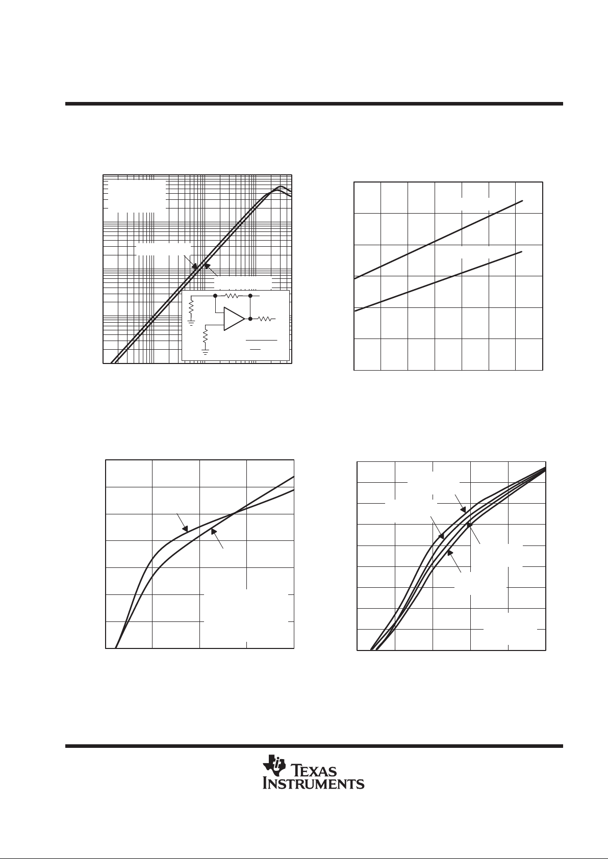
Figure 41
Number of 150-Ω Loads
DIFFERENTIAL GAIN
vs
LOADING
0.08
0.04
0.02
0
26
0.14
1
4
Differential Gain – %
0.12
VCC = ±15 V
35
0.10
0.06
Gain = 2
RF = 680 Ω
40 IRE – NTSC Modulation
Worst Case ±100 IRE Ramp
VCC = ±5 V
Figure 42
Number of 150-Ω Loads
DIFFERENTIAL GAIN
vs
LOADING
0.08
0.04
0.02
0
26
0.16
1
4
Differential Gain – %
0.12
35
0.10
0.06
0.14
VCC = ±15 V
Gain = 2
RF = 680 Ω
40 IRE – PAL Modulation
Worst Case ±100 IRE Ramp
VCC = ±5 V
Figure 43
Number of 150-Ω Loads
DIFFERENTIAL PHASE
vs
LOADING
0.15
0.05
0
26
0.3
1
4
0.25
35
0.2
0.1
Differential Phase –
°
VCC = ±15 V
Gain = 2
RF = 680 Ω
40 IRE – NTSC Modulation
Worst Case ±100 IRE Ramp
VCC = ±5 V
Figure 44
Number of 150-Ω Loads
DIFFERENTIAL PHASE
vs
LOADING
0.2
0.1
0.05
0
26
0.45
1
4
0.3
35
0.25
0.15
0.4
Differential Phase –
°
Gain = 2
RF = 680 Ω
40 IRE – PAL Modulation
Worst Case ±100 IRE Ramp
VCC = ±15 V
VCC = ±5 V
0.35
Page 20

THS6022
250-mA DUAL DIFFERENTIAL LINE DRIVER
SLOS225C – SEPTEMBER 1998 – REVISED JANUARY 2000
20
POST OFFICE BOX 655303 • DALLAS, TEXAS 75265
TYPICAL CHARACTERISTICS
Figure 45
t – Time – ns
400-mV STEP RESPONSE
100
–100
0
–200
V
O
– Output Voltage – mV
300
200
0302010 40 50 7060 80 90 100
400
–300
–400
VCC = ±15 V
Gain = 5
RF = 1 kΩ
RL = 50 Ω
tr/tf = 900 ns
Figure 46
t – Time – ns
20-V STEP RESPONSE
4
–4
0
–8
V
O
– Output Voltage – V
12
8
0302010 40 50 7060 80 90 100
16
–12
–16
Minimal Saturation
VCC = ±15 V
Gain = 5
RF = 1 kΩ
RL = 50 Ω
tr/tf = 7 ns
Figure 47
t – Time – ns
400-mV STEP RESPONSE
100 mV Per Division
0302010 40 50 7060 80 90 100
VCC = ±5 V
Gain = 2
RF = 1 kΩ
tr/tf = 900 ns
See Figure 2
RL = 50 Ω
RL = 25 Ω
Figure 48
t – Time – ns
4-V STEP RESPONSE
1 V Per Division
0302010 40 50 7060 80 90 100
VCC = ±5 V
Gain = 2
RF = 1 kΩ
tr/tf = 900 ns
See Figure 2
RL = 25 Ω
RL = 50 Ω
Page 21

THS6022
250-mA DUAL DIFFERENTIAL LINE DRIVER
SLOS225C – SEPTEMBER 1998 – REVISED JANUARY 2000
21
POST OFFICE BOX 655303 • DALLAS, TEXAS 75265
APPLICATION INFORMATION
simplified schematic
IN+ IN–
V
CC+
V
CC–
OUT
I
bias
I
bias
The THS6022 contains two independent operational amplifiers. These amplifiers are current feedback topology
amplifiers made for high-speed operation. They have been specifically designed to deliver the full power
requirements of ADSL and therefore can deliver output currents of at least 200 mA at full output voltage.
The THS6022 is fabricated using Texas Instruments 30-V complementary bipolar process, HVBiCOM. This
process provides excellent isolation and high slew rates that result in the device’s excellent crosstalk and
extremely low distortion.
independent power supplies
Each amplifier of the THS6022 has its own power supply pins. This was specifically done to solve a problem
that often occurs when multiple devices in the same package share common power pins. This problem is
crosstalk between the individual devices caused by currents flowing in common connections. Whenever the
current required by one device flows through a common connection shared with another device, this current,
in conjunction with the impedance in the shared line, produces an unwanted voltage on the power supply . Proper
power supply decoupling and good device power supply rejection helps to reduce this unwanted signal. What
is left is crosstalk.
Page 22

THS6022
250-mA DUAL DIFFERENTIAL LINE DRIVER
SLOS225C – SEPTEMBER 1998 – REVISED JANUARY 2000
22
POST OFFICE BOX 655303 • DALLAS, TEXAS 75265
independent power supplies (continued)
However, with independent power supply pins for each device, the effects of crosstalk through common
impedance in the power supplies are more easily managed. This is because it is much easier to achieve low
common impedance on the PCB with copper etch than it is to achieve low impedance within the package with
either bond wires or metal traces on silicon.
power supply restrictions
Although the THS6022 is specified for operation from power supplies of ±5 V to ±15 V (or singled-ended power
supply operation from 10 V to 30 V), and each amplifier has its own power supply pins, several precautions must
be taken to assure proper operation.
1. The power supplies for each amplifier must be the same value. For example, if the driver 1 uses ±15 volts,
then the driver 2 must also use ±15 volts. Using ±15 volts for one amplifier and ±5 volts for another amplifier
is not allowed.
2. T o save power by powering down one of the amplifiers in the package, the following rules must be followed.
• The amplifier designated driver 1 must always receive power. This is because the internal startup
circuitry uses the power from the driver 1 device.
• The –V
CC
pins from both drivers must always be at the same potential.
• Individual amplifiers are powered down by simply opening the +V
CC
connection.
The THS6022 incorporates a standard Class A-B output stage. This means that some of the quiescent current
is directed to the load as the load current increases. So under heavy load conditions, accurate power dissipation
calculations are best achieved through actual measurements. For small loads, however, internal power
dissipation for each amplifier in the THS6022 can be approximated by the following formula:
PD≅ǒ2VCCI
CC
Ǔ)ǒ
VCC_V
O
Ǔ
ǒ
V
O
R
L
Ǔ
Where:
P
D
= Power dissipation for one amplifier
VCC= Split supply voltage
I
CC
= Supply current for that particular amplifier
VO= RMS output voltage of amplifier
RL= Load resistance
To find the total THS6022 power dissipation, we simply sum up both amplifier power dissipation results.
Generally , the worst case power dissipation occurs when the output voltage is one-half the V
CC
voltage. One
last note, which is often overlooked: the feedback resistor (RF) is also a load to the output of the amplifier and
should be taken into account for low value feedback resistors.
device protection features
The THS6022 has two built-in features that protect the device against improper operation. The first protection
mechanism is output current limiting. Should the output become shorted to ground the output current is
automatically limited to the value given in the data sheet. While this protects the output against excessive
current, the device internal power dissipation increases due to the high current and large voltage drop across
the output transistors. Continuous output shorts are not recommended and could damage the device.
Additionally , connection of the amplifier output to one of the supply rails (±V
CC
) can cause failure of the device
and is not recommended.
Page 23

THS6022
250-mA DUAL DIFFERENTIAL LINE DRIVER
SLOS225C – SEPTEMBER 1998 – REVISED JANUARY 2000
23
POST OFFICE BOX 655303 • DALLAS, TEXAS 75265
APPLICATION INFORMATION
device protection features (continued)
The second built-in protection feature is thermal shutdown. Should the internal junction temperature rise above
approximately 180_C, the device automatically shuts down. Such a condition could exist with improper heat
sinking or if the output is shorted to ground. When the abnormal condition is fixed, the internal thermal shutdown
circuit automatically turns the device back on.
thermal information
The THS6022 is packaged in a thermally-enhanced PWP package, which is a member of the PowerP AD family
of packages. This package is constructed using a downset leadframe upon which the die is mounted
[see Figure 50(a) and Figure 50(b)]. This arrangement results in the lead frame being exposed as a thermal pad
on the underside of the package [see Figure 50(c)]. Because this thermal pad has direct thermal contact with
the die, excellent thermal performance can be achieved by providing a good thermal path away from the thermal
pad.
The PowerP AD package allows for both assembly and thermal management in one manufacturing operation.
During the surface-mount solder operation (when the leads are being soldered), the thermal pad can also be
soldered to a copper area underneath the package. Through the use of thermal paths within this copper area,
heat can be conducted away from the package into either a ground plane or other heat dissipating device. This
is discussed in more detail in the
PCB design considerations
section of this document.
The PowerPAD package represents a breakthrough in combining the small area and ease of assembly of
surface mount with the, heretofore, awkward mechanical methods of heatsinking.
DIE
Side View (a)
End View (b)
Bottom View (c)
DIE
Thermal
Pad
NOTE A: The thermal pad is electrically isolated from all terminals in the package.
Figure 49. Views of Thermally Enhanced PWP Package
Page 24

THS6022
250-mA DUAL DIFFERENTIAL LINE DRIVER
SLOS225C – SEPTEMBER 1998 – REVISED JANUARY 2000
24
POST OFFICE BOX 655303 • DALLAS, TEXAS 75265
APPLICATION INFORMATION
recommended feedback and gain resistor values
As with all current feedback amplifiers, the bandwidth of the THS6022 is an inversely proportional function of
the value of the feedback resistor. This can be seen from Figures 19 to 32. The recommended resistors for the
optimum frequency response are shown in T able 1. These should be used as a starting point and once optimum
values are found, 1% tolerance resistors should be used to maintain frequency response characteristics.
Because there is a finite amount of output resistance of the operational amplifier, load resistance can play a
major part in frequency response. This is especially true with these drivers, which tend to drive low-impedance
loads. This can be seen in Figure 10 and Figures 25 – 28. As the load resistance increases, the output resistance
of the amplifier becomes less dominant at high frequencies. To compensate for this, the feedback resistor
should change. Although, for most applications, a feedback resistor value of 1 kΩ is recommended, which is
a good compromise between bandwidth and phase margin that yields a very stable amplifier.
Table 1. Recommended Feedback (R
F
) Values for Optium Frequency Response
VCC = ±15 V VCC = ±15 V
GAIN
RL = 50 Ω RL = 100 Ω RL = 25 Ω RL = 50 Ω RL = 100 Ω
1 787 Ω 750 Ω 1 kΩ 910 Ω 820 Ω
2 590 Ω 590 Ω 820 Ω 715 Ω 680 Ω
–1 560 Ω — — 680 Ω —
Consistent with current feedback amplifiers, increasing the gain is best accomplished by changing the gain
resistor, not the feedback resistor . This is because the bandwidth of the amplifier is dominated by the feedback
resistor value and internal dominant-pole capacitor. The ability to control the amplifier gain independently of the
bandwidth constitutes a major advantage of current feedback amplifiers over conventional voltage feedback
amplifiers. Therefore, once a frequency response is found suitable to a particular application, adjust the value
of the gain resistor to increase or decrease the overall amplifier gain.
Finally, it is important to realize the effects of the feedback resistance on distortion. Increasing the resistance
decreases the loop gain and increases the distortion. It is also important to know that decreasing load
impedance increases total harmonic distortion (THD). Typically, the third order harmonic distortion increases
more than the second order harmonic distortion. This is illustrated in Figure 40.
offset voltage
The output offset voltage, (VOO) is the sum of the input offset voltage (VIO) and both input bias currents (IIB) times
the corresponding gains. The following schematic and formula can be used to calculate the output offset
voltage:
VOO+
V
IO
ǒ
1
) ǒ
R
F
R
G
Ǔ
Ǔ
"
I
IB
)
R
S
ǒ
1
) ǒ
R
F
R
G
Ǔ
Ǔ
"
I
IB–RF
+
–
V
I
+
R
G
R
S
R
F
I
IB–
V
O
I
IB+
Figure 50. Output Offset Voltage Model
Page 25

THS6022
250-mA DUAL DIFFERENTIAL LINE DRIVER
SLOS225C – SEPTEMBER 1998 – REVISED JANUARY 2000
25
POST OFFICE BOX 655303 • DALLAS, TEXAS 75265
APPLICATION INFORMATION
noise calculations and noise figure
Noise can cause errors on very small signals. This is especially true for the amplifying small signals. The noise
model for current feedback amplifiers (CFB) is the same as voltage feedback amplifiers (VFB). The only
difference between the two is that the CFB amplifiers generally specify different current noise parameters for
each input, while VFB amplifiers usually only specify one noise current parameter. The noise model is shown
in Figure 52. This model includes all of the noise sources as follows:
• e
n
= Amplifier internal voltage noise (nV/√Hz)
• IN+ = Noninverting current noise (pA/√Hz)
• IN– = Inverting current noise (pA/√Hz)
• e
Rx
= Thermal voltage noise associated with each resistor (eRx = 4 kTRx)
_
+
R
F
R
S
R
G
e
Rg
e
Rf
e
Rs
e
n
IN+
Noiseless
IN–
e
ni
e
no
Figure 51. Noise Model
The total equivalent input noise density (eni) is calculated by using the following equation:
eni+
ǒ
e
n
Ǔ
2
)ǒIN
)
R
S
Ǔ
2
)ǒIN–
ǒRFø
R
G
Ǔ
Ǔ
2
)
4kTRs)
4kTǒRFø
R
G
Ǔ
Ǹ
Where:
k = Boltzmann’s constant = 1.380658 × 10
–23
T = Temperature in degrees Kelvin (273 +°C)
RF || RG = Parallel resistance of RF and R
G
To get the equivalent output noise of the amplifier, just multiply the equivalent input noise density (eni) by the
overall amplifier gain (AV).
eno+
eniAV+
e
ni
ǒ
1
)
R
F
R
G
Ǔ
(Noninverting Case)
As the previous equations show, to keep noise at a minimum, small value resistors should be used. As the
closed-loop gain is increased (by reducing RG), the input noise is reduced considerably because of the parallel
resistance term. This leads to the general conclusion that the most dominant noise sources are the source
resistor (RS) and the internal amplifier noise voltage (en). Because noise is summed in a root-mean-squares
method, noise sources smaller than 25% of the largest noise source can be effectively ignored. This can greatly
simplify the formula and make noise calculations much easier to calculate.
Page 26

THS6022
250-mA DUAL DIFFERENTIAL LINE DRIVER
SLOS225C – SEPTEMBER 1998 – REVISED JANUARY 2000
26
POST OFFICE BOX 655303 • DALLAS, TEXAS 75265
APPLICATION INFORMATION
noise calculations and noise figure (continued)
This brings up another noise measurement usually preferred in RF applications, the noise figure (NF). Noise
figure is a measure of noise degradation caused by the amplifier. The value of the source resistance must be
defined and is typically 50 Ω in RF applications.
NF+10log
ȧ
ȱ
Ȳ
e
2
ni
ǒ
e
Rs
Ǔ
2
ȧ
ȳ
ȴ
Because the dominant noise components are generally the source resistance and the internal amplifier noise
voltage, we can approximate noise figure as:
NF+10log
ȧ
ȧ
ȧ
ȧ
ȧ
ȱ
Ȳ
1
)
ȧ
ȡ
Ȣ
ǒ
e
n
Ǔ
2
)ǒIN
)
R
S
Ǔ
2
ȧ
ȣ
Ȥ
4kTR
S
ȧ
ȧ
ȧ
ȧ
ȧ
ȳ
ȴ
Figure 52 shows the noise figure graph for the THS6022.
NOISE FIGURE
vs
SOURCE RESISTANCE
18
14
0
20
16
12
Noise Figure – dB
Rs – Source Resistance – Ω
10 100 1 k 10 k
TA = 25°C
8
4
10
6
2
Figure 52. Noise Figure vs Source Resistance
Page 27

THS6022
250-mA DUAL DIFFERENTIAL LINE DRIVER
SLOS225C – SEPTEMBER 1998 – REVISED JANUARY 2000
27
POST OFFICE BOX 655303 • DALLAS, TEXAS 75265
APPLICATION INFORMATION
slew rate
The slew rate performance of a current feedback amplifier, like the THS6022, is affected by many different
factors. Some of these factors are external to the device, such as amplifier configuration and PCB parasitics,
and others are internal to the device, such as available currents and node capacitance. Understanding some
of these factors should help the PCB designer arrive at a more optimum circuit with fewer problems.
Whether the THS6022 is used in an inverting amplifier configuration or a noninverting configuration can impact
the output slew rate. Slew rate performance in the inverting configuration is generally faster than the
noninverting configuration. This is because in the inverting configuration the input terminals of the amplifier are
at a virtual ground and do not significantly change voltage as the input changes. Consequently, the time to
charge any capacitance on these input nodes is less than for the noninverting configuration, where the input
nodes actually do change in voltage an amount equal to the size of the input step. In addition, any PCB parasitic
capacitance on the input nodes degrades the slew rate further simply because there is more capacitance to
charge. If the supply voltage (V
CC
) to the amplifier is reduced, slew rate decreases because there is less current
available within the amplifier to charge the capacitance on the input nodes as well as other internal nodes. Also,
as the load resistance decreases, the slew rate typically decreases due to the increasing internal currents, which
slow down the transitions (see Figures 13 and 14)
Internally , the THS6022 has other factors that impact the slew rate. The amplifier’s behavior during the slew rate
transition varies slightly depending upon the rise time of the input. This is because of the way the input stage
handles faster and faster input edges. Slew rates (as measured at the amplifier output) of less than about
1300 V/µs are processed by the input stage in a very linear fashion. Consequently, the output waveform
smoothly transitions between initial and final voltage levels. This is shown in Figure 53. For slew rates greater
than 1300 V/µs, additional slew-enhancing transistors present in the input stage begin to turn on to support
these faster signals. The result is an amplifier with extremely fast slew rate capabilities. Figure 54 shows
waveforms for these faster slew rates. The additional aberrations present in the output waveform with these
faster slewing input signals are due to the brief saturation of the internal current mirrors. This phenomenon,
which typically lasts less than 20 ns, is considered normal operation and is not detrimental to the device in any
way . If for any reason this type of response is not desired, then increasing the feedback resistor or slowing down
the input signal slew rate reduces the effect.
Figure 53
t – Time – ns
SLEW RATE — SATURATION
4
–4
0
–8
12
8
0302010 40 50 7060 80 90 100
16
–12
–16
– Output Voltage – V
V
O
SR = 3500 V/µs
VCC = ±15 V
Gain = 5
RL = 1 kΩ
RF = 50 Ω
tr/tf = 900 ns
Figure 54
t – Time – ns
SLEW RATE — LINEAR
4
–4
0
–8
12
8
0302010 40 50 7060 80 90 100
16
–12
–16
– Output Voltage – V
V
O
SR ≅ 1300 V/µs
VCC = ±15 V
Gain = 5
RF = 1 kΩ
RL = 50 Ω
tr/tf = 10 ns
Page 28

THS6022
250-mA DUAL DIFFERENTIAL LINE DRIVER
SLOS225C – SEPTEMBER 1998 – REVISED JANUARY 2000
28
POST OFFICE BOX 655303 • DALLAS, TEXAS 75265
APPLICATION INFORMATION
driving a capacitive load
Driving capacitive loads with high performance amplifiers is not a problem as long as certain precautions are
taken. The first is to realize that the THS6022 has been internally compensated to maximize its bandwidth and
slew rate performance. When the amplifier is compensated in this manner, capacitive loading directly on the
output will decrease the device’s phase margin leading to high frequency ringing or oscillations. Therefore, for
capacitive loads of greater than 10 pF, it is recommended that a resistor be placed in series with the output of
the amplifier, as shown in Figure 55. A minimum value of 15 Ω should work well for most applications. For
example, in 75-Ω transmission systems, setting the series resistor value to 75 Ω both isolates any capacitance
loading and provides the proper line impedance matching at the source end.
+
_
THS6022
C
LOAD
1 kΩ
Input
Output
1 kΩ
15 Ω
Figure 55. Driving a Capacitive Load
PCB design considerations
Proper PCB design techniques in two areas are important to assure proper operation of the THS6022. These
areas are high-speed layout techniques and thermal-management techniques. Because the THS6022 is a
high-speed part, the following guidelines are recommended.
D
Ground plane – It is essential that a ground plane be used on the board to provide all components with a
low inductive ground connection. Although a ground connection directly to a terminal of the THS6022 is not
necessarily required, it is recommended that the thermal pad of the package be tied to ground. This serves
two functions. It provides a low inductive ground to the device substrate to minimize internal crosstalk and
it provides the path for heat removal.
D
Input stray capacitance – To minimize potential problems with amplifier oscillation, the capacitance at the
inverting input of the amplifiers must be kept to a minimum. T o do this, PCB trace runs to the inverting input
must be as short as possible, the ground plane must be removed under any etch runs connected to the
inverting input, and external components should be placed as close as possible to the inverting input. This
is especially true in the noninverting configuration. An example of this can be seen in Figure 56, which shows
what happens when a 1.0 pF capacitor is added to the inverting input terminal in the noninverting
configuration. The bandwidth increases dramatically at the expense of peaking. This is because some of
the error current is flowing through the stray capacitor instead of the inverting node of the amplifier. While
the device is in the inverting mode, stray capacitance at the inverting input has a minimal effect. This is
because the inverting node is at a virtual ground and the voltage does not fluctuate nearly as much as in
the noninverting configuration. This can be seen in Figure 57, where a 27-pF capacitor adds only 0.5 dB
of peaking. In general, as the gain of the system increases, the output peaking due to this capacitor
decreases. While this can initally appear to be a faster and better system, overshoot and ringing are more
likely to occur under fast transient conditions. So, proper analysis of adding a capacitor to the inverting input
node should always be performed for stable operation.
Page 29

THS6022
250-mA DUAL DIFFERENTIAL LINE DRIVER
SLOS225C – SEPTEMBER 1998 – REVISED JANUARY 2000
29
POST OFFICE BOX 655303 • DALLAS, TEXAS 75265
APPLICATION INFORMATION
PCB design considerations (continued)
Figure 56
–6
100 k
–5
OUTPUT AMPLITUDE
vs
FREQUENCY
3
500 M
f – Frequency – Hz
–1
1
2
–4
–3
1 M 10 M 100 M
0
–2
Output Amplitude – dB
VCC = ±15 V
Gain = 1
RL = 50 Ω
VO = 0.2 V
Ci = 0 pF
(Stray C Only)
Ci = 1 pF
1 kΩ
C in
V
I
+
–
V
O
50 Ω
50 Ω
Figure 57
–7
100 k
–6
OUTPUT AMPLITUDE
vs
FREQUENCY
2
500 M
f – Frequency – Hz
–2
0
1
–5
–4
1 M 10 M 100 M
–1
–3
Output Amplitude – dB
VCC = ±15 V
Gain = –1
RL = 50 Ω
VO = 0.2 V
Ci = 27 pF
Ci = 0 pF
(Stray C Only)
1 kΩ
C in
V
I
+
–
V
O
RL = 50 Ω
50 Ω
1 kΩ
D
Proper power supply decoupling – Use a minimum of a 6.8-µF tantalum capacitor in parallel with a 0.1-µF
ceramic capacitor on each supply terminal. It may be possible to share the tantalum among several
amplifiers depending on the application, but a 0.1-µF ceramic capacitor should always be used on the
supply terminal of every amplifier. In addition, the 0.1-µF capacitor should be placed as close as possible
to the supply terminal. As this distance increases, the inductance in the connecting etch makes the capacitor
less effective. The designer should strive for distances of less than 0.1 inches between the device power
terminal and the ceramic capacitors.
Because of its power dissipation, proper thermal management of the THS6022 is required. Although there are
many ways to properly heatsink this device, the following steps illustrate one recommended approach for a
multilayer PCB with an internal ground plane. Refer to Figure 58 for the following steps.
Thermal pad area (0.15 x 0.17) with 6 vias
(Via diameter = 13 mils)
Figure 58. PowerPAD PCB Etch and Via Pattern – Minimum Requirements
Page 30

THS6022
250-mA DUAL DIFFERENTIAL LINE DRIVER
SLOS225C – SEPTEMBER 1998 – REVISED JANUARY 2000
30
POST OFFICE BOX 655303 • DALLAS, TEXAS 75265
APPLICATION INFORMATION
PCB design considerations (continued)
1. Place 6 holes in the area of the thermal pad. These holes should be 13 mils in diameter. They are kept small
so that solder wicking through the holes is not a problem during reflow.
2. Additional vias may be placed anywhere along the thermal plane outside of the thermal pad area. This will
help dissipate the heat generated from the THS6022. These additional vias may be larger than the 13 mil
diameter vias directly under the thermal pad. They can be larger because they are not in the thermal-pad
area to be soldered, therefore, wicking is generally not a problem.
3. Connect all holes to the internal ground plane.
4. When connecting these holes to the ground plane, do not use the typical web or spoke via connection
methodology . Web connections have a high thermal resistance connection that is useful for slowing the heat
transfer during soldering operations. This makes the soldering of vias that have plane connections easier.
However, in this application, low thermal resistance is desired for the most ef ficient heat transfer. Therefore,
the holes under the THS6022 package should make their connection to the internal ground plane with a
complete connection around the entire circumference of the plated through hole.
5. The top-side solder mask should leave exposed the terminals of the package and the thermal pad area with
its 6 holes. The bottom-side solder mask should cover the 6 holes of the thermal pad area. This eliminates
the solder from being pulled away from the thermal pad area during the reflow process.
6. Apply solder paste to the exposed thermal pad area and all of the operational amplifier terminals.
7. With these preparatory steps in place, the THS6022 is simply placed in position and run through the solder
reflow operation as any standard surface-mount component. This results in a part that is properly installed.
The actual thermal performance achieved with the THS6022 in its PowerPAD package depends on the
application. In the example above, if the size of the internal ground plane is approximately 3 inches × 3 inches,
then the expected thermal coefficient, θJA, is about 37.5°C/W. For a given θJA, the maximum power dissipation
is shown in Figure 60 and is calculated by the following formula:
PD+
ǒ
T
MAX–TA
q
JA
Ǔ
Where:
PD= Maximum power dissipation of THS6022 (watts)
T
MAX
= Absolute maximum junction temperature (150°C)
TA= Free-ambient air temperature (°C)
θ
JA
= θJC + θCA
θJC = Thermal coefficient from junction to case (2.07°C/W)
θCA = Thermal coefficient from case to ambient air
Page 31

THS6022
250-mA DUAL DIFFERENTIAL LINE DRIVER
SLOS225C – SEPTEMBER 1998 – REVISED JANUARY 2000
31
POST OFFICE BOX 655303 • DALLAS, TEXAS 75265
APPLICATION INFORMATION
PCB design considerations (continued)
More complete details of the PowerP AD installation process and thermal management techniques can be found
in the T exas Instruments technical brief,
PowerP AD Thermally Enhanced Package.
This document can be found
at the TI web site (www.ti.com) by searching on the key word PowerPAD. The document can also be ordered
through your local TI sales office. Refer to literature number SLMA002 when ordering.
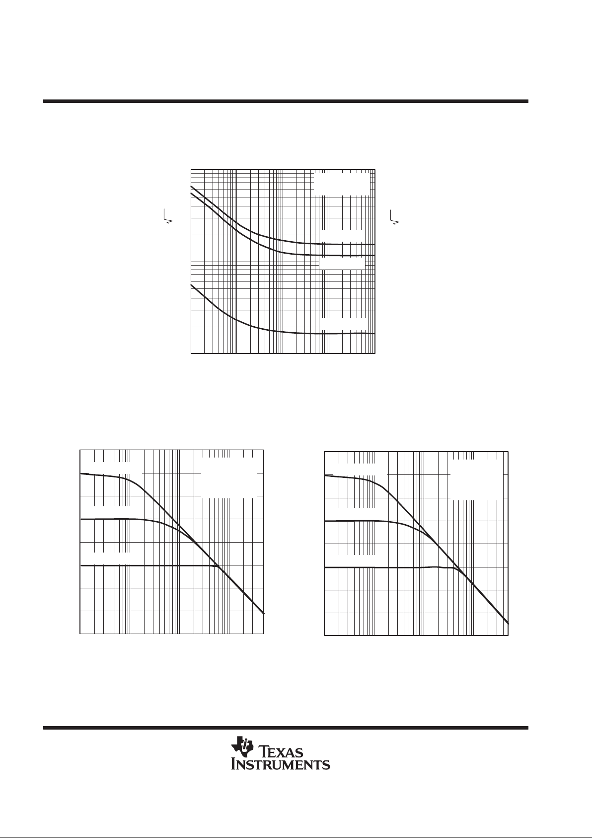
TA – Free-Air Temperature – °C
–40 –20 0 20 80 1006040
MAXIMUM POWER DISSIPATION
vs
FREE-AIR TEMPERATURE
5
3
1
0
4
2
6
Maximum Power Dissipation – W
TJ = 150°C
PCB Size = 3” x 3”
No Air Flow
θJA = 37.5°C/W
2 oz Trace and
Copper Pad
with Solder
θJA = 97.7°C/W
2 oz Trace and Copper Pad
without Solder
Figure 59. Maximum Power Dissipation vs Free-Air Temperature
Page 32

THS6022
250-mA DUAL DIFFERENTIAL LINE DRIVER
SLOS225C – SEPTEMBER 1998 – REVISED JANUARY 2000
32
POST OFFICE BOX 655303 • DALLAS, TEXAS 75265
APPLICATION INFORMATION
ADSL
The THS6022 was primarily designed as a line driver and line receiver for ADSL (asymmetrical digital subscriber
line). The driver output stage has been sized to provide full ADSL power levels of 13 dBm onto the telephone
lines. Although actual driver output peak voltages and currents vary with each particular ADSL application, the
THS6022 is specified for a minimum full output current of 200 mA at its full output voltage of approximately 12
V . This performance meets the demanding needs of ADSL at the client side end of the telephone line. A typical
ADSL schematic is shown in Figure 60.
_
+
6.8 µF0.1 µF
–15 V
6.8 µF0.1 µF
15 V
1 kΩ
1 kΩ
+
+
V
I+
_
+
6.8 µF0.1 µF
–15 V
6.8 µF0.1 µF
15 V
1 kΩ
1 kΩ
+
+
V
I–
+
–
1 kΩ
0.1 µF
1 kΩ
2 kΩ
50 Ω
+
–
1 kΩ
0.1 µF
1 kΩ
2 kΩ
1:1
Telephone Line
50 Ω
–15 V
15 V
15 V
–15 V
0.01 µF
THS6062
Receiver 1
THS6062
Receiver 2
V
O+
V
O–
THS6022
Driver 1
THS6022
Driver 2
100 Ω
Figure 60. THS6022 ADSL Application
Page 33

THS6022
250-mA DUAL DIFFERENTIAL LINE DRIVER
SLOS225C – SEPTEMBER 1998 – REVISED JANUARY 2000
33
POST OFFICE BOX 655303 • DALLAS, TEXAS 75265
APPLICATION INFORMATION
ADSL (continued)
The ADSL transmit band consists of 255 separate carrier frequencies each with its own modulation and
amplitude level. With such an implementation, it is imperative that signals put onto the telephone line have as
low a distortion as possible. This is because any distortion either interferes directly with other ADSL carrier
frequencies or it creates intermodulation products that interfere with ADSL carrier frequencies.
The THS6022 has been specifically designed for ultra low distortion by careful circuit implementation and by
taking advantage of the superb characteristics of the complementary bipolar process. Driver single-ended
distortion measurements are shown in Figures 37 – 40. It is commonly known that in the differential driver
configuration, the second order harmonics tend to cancel out. Thus, the dominant total harmonic distortion
(THD) will be primarily due to the third order harmonics. Additionally, distortion should be reduced as the
feedback resistance drops. This is because the bandwidth of the amplifier increases, which allows the amplifier
to react faster to any nonlinearities in the closed-loop system.
Another significant point is the fact that distortion decreases as the impedance load increases. This is because
the output resistance of the amplifier becomes less significant as compared to the output load resistance. This
is illustrated by Figure 40.
One problem that has been receiving a lot of attention in the ADSL area is power dissipation. One way to
substantially reduce power dissipation is to lower the power supply voltages. This is because the RMS voltage
of an ADSL remote terminal signal is 1.35-V RMS. But, to meet ADSL requirements, the drivers must have a
voltage RMS-to-peak crest factor of 5.6 in order to keep the bit-error probability rate below 10
–7
. Hence, the
power supply voltages must be high enough to accomplish the peak output voltage of 1.35 V × 5.6 = 7.6 V
(PEAK)
.
If ±15-V power supplies are used for the THS6022 drivers in the circuit shown in Figure 61, the power dissipation
of the THS6022 is approximately 600 mW. This is assuming that part of the quiescent current is diverted back
to the load, which typically happens in a class-AB amplifier. But, if the power supplies are dropped down to
±12 V, then the power dissipation drops to appriximately 460 mW. This is a 23% reduction of power, which
ultimately lowers the temperature of the drivers and increases efficiency.
Another way to reduce power dissipation in the drivers is to increase the transformer ratio. The drawback in
doing this is that it increases the loading on the drivers and reduces the signals being received from the central
office. If this can be overcome, then a power reduction in the drivers will result. By going to a 1:2 transformer
ratio, the power supply voltages can drop to ±6 V . The driver output voltage has now been reduced to 675-mV
RMS. But, the loading on the output of the drivers drops to 25 Ω. The power dissipated is now approximately
360 mW, a reduction of 22% over the previous example. But, the received signal is now 1/2 of the previous
example. This must be dealt with by requiring low-noise receivers. There are always trade offs when it comes
to dealing with power, so proper analysis of the system should always be considered.
general configurations
A common error for the first-time CFB user is to create a unity gain buffer amplifier by shorting the output directly
to the inverting input. A CFB amplifier in this configuration oscillates and is not recommended. The THS6022,
like all CFB amplifiers, must have a feedback resistor for stable operation. Additionally, placing capacitors
directly from the output to the inverting input is not recommended. This is because, at high frequencies, a
capacitor has a very low impedance. This results in an unstable amplifier and should not be considered when
using a current-feedback amplifier. Because of this, integrators and simple low-pass filters, which are easily
implemented on a VFB amplifier, have to be designed slightly dif ferently . If filtering is required, simply place an
RC-filter at the noninverting terminal of the operational-amplifier (see Figure 62).
Page 34

THS6022
250-mA DUAL DIFFERENTIAL LINE DRIVER
SLOS225C – SEPTEMBER 1998 – REVISED JANUARY 2000
34
POST OFFICE BOX 655303 • DALLAS, TEXAS 75265
APPLICATION INFORMATION
general configurations (continued)
V
I
V
O
C1
+
–
R
G
R
F
R1
f
–3dB
+
1
2pR1C1
V
O
V
I
+ ǒ
1
)
R
F
R
G
Ǔ
ǒ
1
1)sR1C1
Ǔ
Figure 61. Single-Pole Low-Pass Filter
If a multiple pole filter is required, the use of a Sallen-Key filter can work very well with CFB amplifiers. This is
because the filtering elements are not in the negative feedback loop and stability is not compromised. Because
of their high slew-rates and high bandwidths, CFB amplifiers can create very accurate signals and help minimize
distortion. An example is shown in Figure 63.
V
I
C2
R2R1
C1
R
F
R
G
R1 = R2 = R
C1 = C2 = C
Q = Peaking Factor
(Butterworth Q = 0.707)
(
=
1
Q
2 –
)
R
G
R
F
_
+
f
–3dB
+
1
2pRC
Figure 62. 2-Pole Low-Pass Sallen-Key Filter
There are two simple ways to create an integrator with a CFB amplifier. The first one, shown in Figure 64, adds
a resistor in series with the capacitor. This is acceptable because at high frequencies, the resistor is dominant
and the feedback impedance never drops below the resistor value. The second one, shown in Figure 65, uses
positive feedback to create the integration. Caution is advised because oscillations can occur because of the
positive feedback.
+
–
C1
R
F
R
G
V
O
V
I
THS6022
V
O
V
I
+ ǒ
R
F
R
G
Ǔ
ȧ
ȡ
Ȣ
S
)
1
RFC1
S
ȧ
ȣ
Ȥ
Figure 63. Inverting CFB Integrator
Page 35

THS6022
250-mA DUAL DIFFERENTIAL LINE DRIVER
SLOS225C – SEPTEMBER 1998 – REVISED JANUARY 2000
35
POST OFFICE BOX 655303 • DALLAS, TEXAS 75265
APPLICATION INFORMATION
general configurations (continued)
+
–
R
F
V
O
R
G
R2R1
C1
R
A
V
I
THS6022
For Stable Operation:
R2
R1 || R
A
≥
R
F
R
G
sR1C1
(
)
R
F
R
G
1 +
VO
≅ V
I
Figure 64. Noninverting CFB Integrator
Another good use for the THS6022 amplifiers is as very good video distribution amplifiers. One characteristic
of distribution amplifiers is the fact that the differential phase (DP) and the differential gain (DG) are
compromised as the number of lines increases and the closed-loop gain increases. Be sure to use termination
resistors throughout the distribution system to minimize reflections and capacitive loading.
+
–
715 Ω715 Ω
75 Ω
75 Ω
75 Ω
75 Ω
75 Ω
N Lines
V
O1
V
ON
THS6022
75 Ω Transmission Line
V
I
+5 V
–5 V
Figure 65. Video Distribution Amplifier Application
evaluation board
An evaluation board is available for the THS6022 (literature number SLOP133). This board has been configured
for proper thermal management of the THS6022. The circuitry has been designed for a typical ADSL application
as shown previously in this document. For more detailed information, refer to the
THS6022EVM User’s Manual
(literature number SLOV035) To order the evaluation board, contact your local TI sales office or distributor.
Page 36

THS6022
250-mA DUAL DIFFERENTIAL LINE DRIVER
SLOS225C – SEPTEMBER 1998 – REVISED JANUARY 2000
36
POST OFFICE BOX 655303 • DALLAS, TEXAS 75265
MECHANICAL INFORMATION
PWP (R-PDSO-G**) PowerPAD PLASTIC SMALL-OUTLINE PACKAGE
4073225/E 03/97
0,50
0,75
0,25
0,15 NOM
Thermal Pad
(See Note D)
Gage Plane
2824
7,70
7,90
20
6,40
6,60
9,60
9,80
6,60
6,20
11
0,19
4,50
4,30
10
0,15
20
A
1
0,30
1,20 MAX
1614
5,10
4,90
PINS **
4,90
5,10
DIM
A MIN
A MAX
0,05
Seating Plane
0,65
0,10
M
0,10
0°–8°
20-PIN SHOWN
NOTES: A. All linear dimensions are in millimeters.
B. This drawing is subject to change without notice.
C. Body dimensions do not include mold flash or protrusions.
D. The package thermal performance may be enhanced by bonding the thermal pad to an external thermal plane. This pad is electrically
and thermally connected to the backside of the die and possibly selected leads.
E. Falls within JEDEC MO-153
PowerPAD is a trademark of Texas Instruments Incorporated.
Page 37

THS6022
250-mA DUAL DIFFERENTIAL LINE DRIVER
SLOS225C – SEPTEMBER 1998 – REVISED JANUARY 2000
37
POST OFFICE BOX 655303 • DALLAS, TEXAS 75265
MECHANICAL DATA
GQE (S-PLGA-N80) PLASTIC LAND GRID ARRAY
98765
J
H
G
F
E
D
321
C
B
A
4
4,00 TYP
Seating Plane
5,20
4,80
SQ
0,87
0,93
0,08 MAX
0,23
0,33
1,00 MAX
0,50
0,50
0,08
M
∅ 0,05
4200461/A 10/99
NOTES: A. All linear dimensions are in millimeters.
B. This drawing is subject to change without notice.
C. MicroStar Junior LGA configuration
MicroStar Junior LGA is a trademark of Texas Instruments Incorporated.
Page 38

IMPORTANT NOTICE
T exas Instruments and its subsidiaries (TI) reserve the right to make changes to their products or to discontinue
any product or service without notice, and advise customers to obtain the latest version of relevant information
to verify, before placing orders, that information being relied on is current and complete. All products are sold
subject to the terms and conditions of sale supplied at the time of order acknowledgement, including those
pertaining to warranty, patent infringement, and limitation of liability.
TI warrants performance of its semiconductor products to the specifications applicable at the time of sale in
accordance with TI’s standard warranty. Testing and other quality control techniques are utilized to the extent
TI deems necessary to support this warranty. Specific testing of all parameters of each device is not necessarily
performed, except those mandated by government requirements.
CERT AIN APPLICATIONS USING SEMICONDUCTOR PRODUCTS MAY INVOLVE POTENTIAL RISKS OF
DEATH, PERSONAL INJURY, OR SEVERE PROPERTY OR ENVIRONMENTAL DAMAGE (“CRITICAL
APPLICATIONS”). TI SEMICONDUCTOR PRODUCTS ARE NOT DESIGNED, AUTHORIZED, OR
WARRANTED TO BE SUITABLE FOR USE IN LIFE-SUPPORT DEVICES OR SYSTEMS OR OTHER
CRITICAL APPLICATIONS. INCLUSION OF TI PRODUCTS IN SUCH APPLICA TIONS IS UNDERSTOOD T O
BE FULLY AT THE CUSTOMER’S RISK.
In order to minimize risks associated with the customer’s applications, adequate design and operating
safeguards must be provided by the customer to minimize inherent or procedural hazards.
TI assumes no liability for applications assistance or customer product design. TI does not warrant or represent
that any license, either express or implied, is granted under any patent right, copyright, mask work right, or other
intellectual property right of TI covering or relating to any combination, machine, or process in which such
semiconductor products or services might be or are used. TI’s publication of information regarding any third
party’s products or services does not constitute TI’s approval, warranty or endorsement thereof.
Copyright 2000, Texas Instruments Incorporated
 Loading...