

Page 1
SLOS388B – OCTOBER 2001 – REVISED JUNE 2002
WIDEBAND, FET-INPUT OPERATIONAL AMPLIFIER
THS4601
FEATURES
Gain Bandwidth Product: 180 MHz
D
D Slew Rate: 100 V/µs
D Maximum Input Bias Current: 100 pA
D Input Voltage Noise: 5.4 nV/√Hz
D Maximum Input Offset Voltage: 4 mV
D Input Impedance: 10
9
Ω || 10 pF
D Power Supply Voltage Range: ±5 to ±15 V
D Unity Gain Stable
APPLICATIONS
D
Wideband Photodiode Amplifier
D High-Speed Transimpedance Gain Stage
D Test and Measurement Systems
D Current-DAC Output Buffer
D Active Filtering
D High-Speed Signal Integrator
D High-Impedance Buffer
A SELECTION OF RELATED OPERATIONAL AMPLIFIER PRODUCTS
DESCRIPTION
The THS4601 is a high-speed, FET-input operational
amplifier designed for applications requiring wideband
operation, high-input impedance, and high-power
supply voltages. By providing a 180-MHz gainbandwidth product, ±15-V supply operation, and
100-pA input bias current, the THS4601 is capable of
wideband transimpedance gain and large output signal
swing simultaneously. Low current and voltage noise
allow amplification of extremely low-level input signals
while still maintaining a large signal-to-noise ratio.
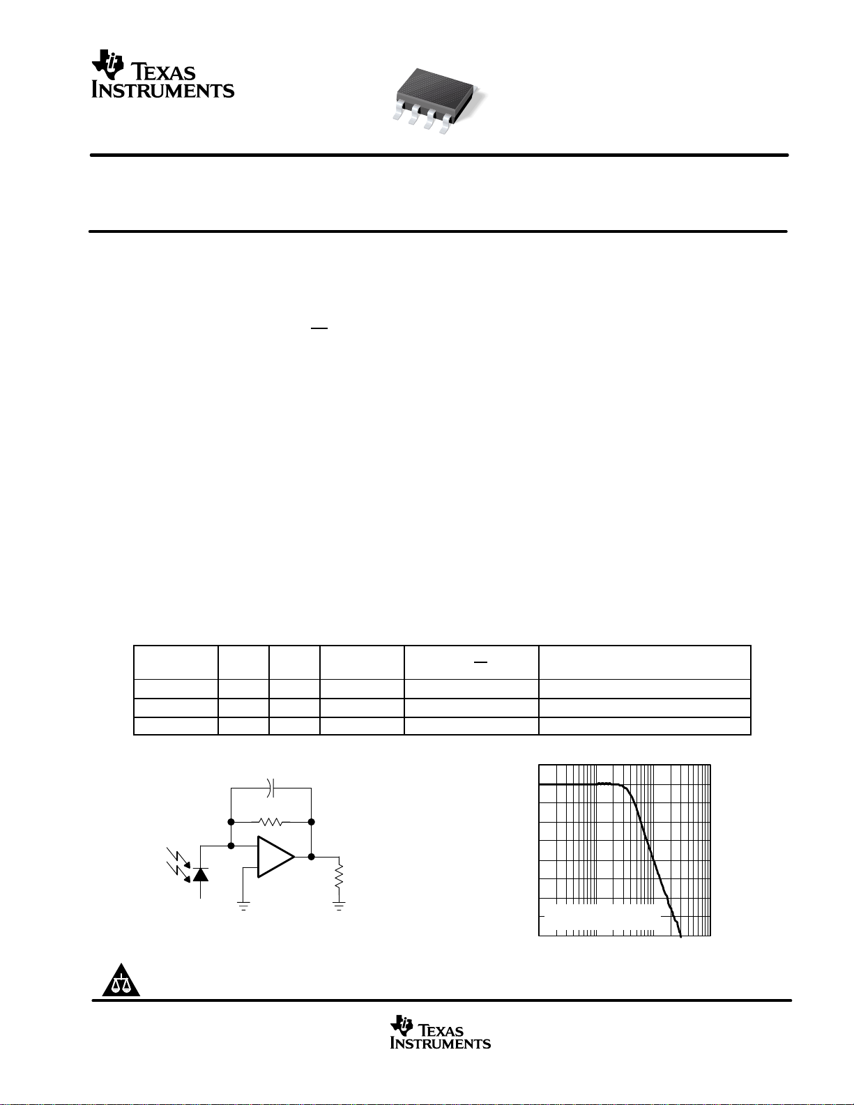
The characteristics of the THS4601 ideally suit it for use
as a wideband photodiode amplifier. Photodiode output
current is a prime candidate for transimpedance
amplification, an application of which is illustrated in
Figure 1. Other potential applications include test and
measurement systems requiring high-input impedance,
digital-to-analog converter output buffering, high-speed
integration, and active filtering.
DEVICE
OPA627
OPA637 ±15 80 135 4.5 Gain of +5 stable FET-input amplifier
OPA655 ±5 400 290 6 Unity-gain stable FET-input amplifier
λ
–V
V
(V)
±15
18 pF
Bias
S
C
= 0.7 pF
F
R
= 100 kΩ
F
_
+
BW
(MHz)
16 55 4.5 Unity-gain stable FET-input amplifier
THS4601
Figure 1. Wideband Photodiode
Transimpedance Amplifier
Please be aware that an important notice concerning availability, standard warranty, and use in critical applications of
Texas Instruments semiconductor products and disclaimers thereto appears at the end of this data sheet.
PRODUCTION DATA information is current as of publication date.
Products conform to specifications per the terms of Texas Instruments
standard warranty. Production processing does not necessarily include
testing of all parameters.
SLEW RATE
(V/µs)
RL = 1 kΩ
VOLTAGE NOISE
(nV√Hz
www.ti.com
)
100 kΩ TRANSIMPEDANCE BANDWIDTH
105
100
95
90
85
80
75
70
Transimpedance Gain – dB
Diode Capacitance: 18 pF
65
–3 dB Bandwidth: 4 MHz
60
0.1 1 10 100
DESCRIPTION
Frequency – MHz
Copyright 2002, Texas Instruments Incorporated
1
Page 2
THS4601
SLOS388B – OCTOBER 2001 – REVISED JUNE 2002
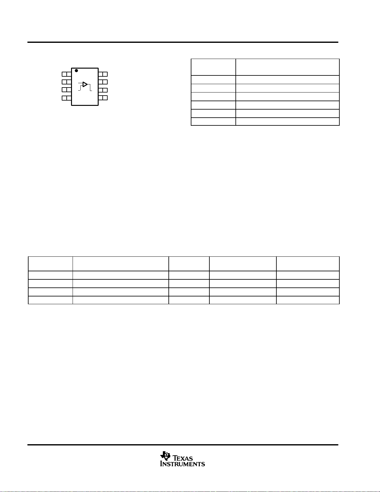
THS4601
D AND DDA PACKAGE
(TOP VIEW)
NC
IN–
IN+
V
S–
NC – No internal connection
1
2
3
4
8
7
6
5
NC
V
S+
OUT
NC
TERMINAL
NAME NO.
NC 1, 5, 8 These pins have no internal connection.
IN– 2 Inverting input of the amplifier
IN+ 3 Noninverting input of the amplifier
V
S–
OUT 6 Output of the amplifier
V
S+
absolute maximum ratings over operating free-air temperature (unless otherwise noted)
Supply voltage, V
Supply voltage, V
Input voltage, V
Output current, I
Differential input voltage, V
Maximum junction temperature, T
Operating free-air temperature, T
S+
S–
. . . . . . . . . . . . . . . . . . . . . . . . . . . . . . . . . . . . . . . . . . . . . . . . . . . . . . . . . . . . . . . . . . . . . . . . . . . . . . . . .
I
O
ID
J
C-suffix 0°C to 70°C. . . . . . . . . . . . . . . . . . . . . . . . . . . . . . . . . . . . . . . . . . . . . . . .
A:
Terminal Functions
DESCRIPTION
4 Negative power supply
7 Positive power supply
†
16.5 V. . . . . . . . . . . . . . . . . . . . . . . . . . . . . . . . . . . . . . . . . . . . . . . . . . . . . . . . . . . . . . . . . . . . . . . . . . .
–16.5 V. . . . . . . . . . . . . . . . . . . . . . . . . . . . . . . . . . . . . . . . . . . . . . . . . . . . . . . . . . . . . . . . . . . . . . . . . .
100 mA. . . . . . . . . . . . . . . . . . . . . . . . . . . . . . . . . . . . . . . . . . . . . . . . . . . . . . . . . . . . . . . . . . . . . . . . . . . .
±4 V. . . . . . . . . . . . . . . . . . . . . . . . . . . . . . . . . . . . . . . . . . . . . . . . . . . . . . . . . . . . . . . . . . . . .
150°C. . . . . . . . . . . . . . . . . . . . . . . . . . . . . . . . . . . . . . . . . . . . . . . . . . . . . . . . . . . . . .
I-suffix –40°C to 85°C. . . . . . . . . . . . . . . . . . . . . . . . . . . . . . . . . . . . . . . . . . . . . . .
Storage temperature, T
stg
–65°C to 125°C. . . . . . . . . . . . . . . . . . . . . . . . . . . . . . . . . . . . . . . . . . . . . . . . . . . . . . . . . . . . . .
Lead temperature 1,6 mm (1/16 inch) from cases for 10 seconds 300°C. . . . . . . . . . . . . . . . . . . . . . . . . . . . . . . . . . . .
†
Stresses beyond those listed under “absolute maximum ratings” may cause permanent damage to the device. These are stress ratings only, and
functional operation of the device at these or any other conditions beyond those indicated under “recommended operating conditions” is not
implied. Exposure to absolute-maximum-rated conditions for extended periods may affect device reliability.
±V
S
PACKAGE AND ORDERING INFORMATION
PRODUCT
THS4601CD SOIC surface mount 8D 0°C to 70°C 4601C
THS4601ID SOIC surface mount 8D –40°C to 85°C 4601I
THS4601CDDA SOIC surface mount with PowerPAD 8DDA 0°C to 70°C 4601C
THS4601IDDA SOIC surface mount with PowerPAD 8DDA –40°C to 85°C 4601I
NOTE: The THS4601 is available taped and reeled. Add an R suffix to the device type when ordering (e.g., THS4601IDR).
PACKAGE
PACKAGE
DESIGNATOR
SPECIFIED
TEMPERATURE RANGE
PACKAGE MARKING
PowerPAD is a trademark of Texas Instruments.
2
www.ti.com
Page 3

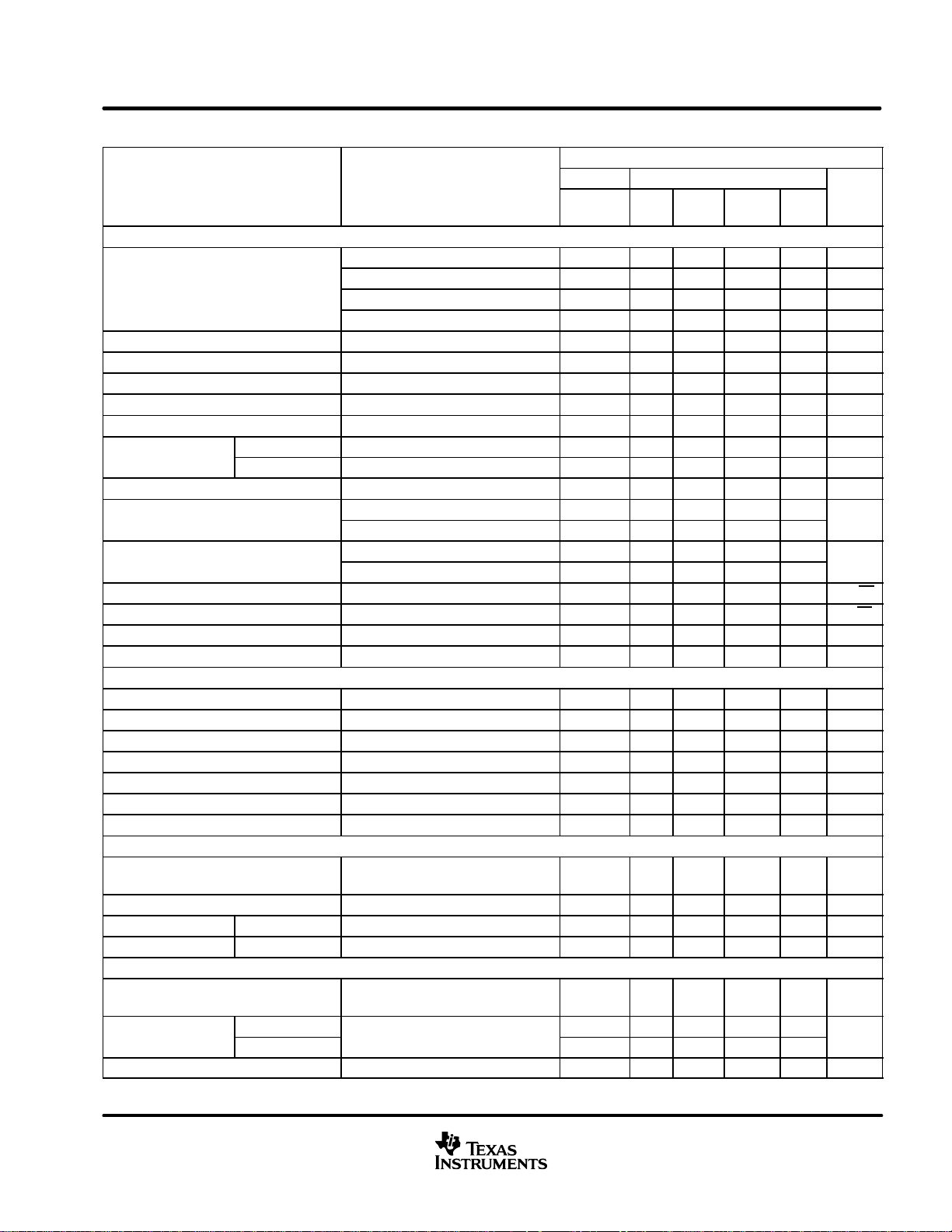
PARAMETER
TEST CONDITIONS
g
d
d
SLOS388B – OCTOBER 2001 – REVISED JUNE 2002
THS4601
electrical specifications: VS = ±15 V: RF = 250 Ω, RL = 1 kΩ and G = +2 (unless otherwise noted)
THS4601
TYP OVER TEMPERATURE
UNIT
dBc
dBc
12.6
to
–12.0
0°C to
70°C
12.5 to
–11.9
25°C 25°C
AC PERFORMANCE
G = +1, VO = 20 mVpp, RF = 0 Ω 440 Typ MHz
G = +2, VO = 40 mVpp, RF = 62 Ω 95 Typ MHz
Small-signal bandwidth
Gain-bandwidth product G > +10 180 Typ MHz
Bandwidth for 0.1 dB flatness G = +2, VO = 200 mV
Large-signal bandwidth G = +5, VO = 10 V
Slew rate, SR G = +5, 10 V Step 100 Typ V/µs
Rise/fall time, tr/t
Settling time, t
Harmonic distortion G = +2, f = 1 MHz, VO = 2V
n
2
r
3
Harmonic
Input voltage noise, V
Input current noise, I
Differential gain (NTSC, P AL) G = +2, RL = 150 Ω 0.02% Typ
Differential phase (NTSC, P AL) G = +2, RL = 150 Ω 0.08 Typ _
DC PERFORMANCE
Open-loop voltage gain G = –10, RL = 1 kΩ 105 94 92 90 Min dB
Input offset voltage, V
Average offset voltage drift VCM = 0 V ±10 ±10 Typ µV/_C
Input bias current, I
Average bias current drift VCM = 0 V 50 50 Typ pA/°C
Input offset current, I
Average offset current drift VCM = 0 V 5 5 Typ pA/°C
INPUT
Common-mode input range, V
Common-mode rejection ratio, CMRR 110 100 95 90 Min dB
Input impedance, ZidDifferential 109 || 3.5 Typ Ω || pF
Input impedance, ZicCommon-mode 109 || 6.5 Typ Ω || pF
s
Harmonic
f
0.01% G = +5, VO = 5 V Step 170 Typ ns
0.1% G = +5, VO = 5 V Step 135 Typ ns
n
n
IO
IB
IO
IC
G = +5, VO = 100 mVpp, RF = 500 Ω 36 Typ MHz
G = +10, VO = 200 mVpp,
RF = 1 kΩ
pp
pp
1.0 V Step 7 Typ ns
pp
RL = 100 Ω –65 Typ
RL = 1 kΩ –77 Typ
RL = 100 Ω –73 Typ
RL = 1 kΩ –96 Typ
f > 10 kHz 5.4 Typ nV/√Hz
f > 10 kHz 5.5 Typ fA/√Hz
VCM = 0 V 1.0 4.0 4.5 5.0 Max mV
VCM = 0 V 30 100 550 1100 Max pA
VCM = 0 V 2 100 200 300 Max pA
18 Typ MHz
5 Typ MHz
3 Typ MHz
±13.0
–40°C
to 85°C
12.4 to
–11.8
MIN/
MAX
Min V
www.ti.com
3
Page 4

THS4601
PARAMETER
TEST CONDITIONS
SLOS388B – OCTOBER 2001 – REVISED JUNE 2002
electrical specifications: VS = ±15 V: RF = 250 Ω, RL = 1kΩ and G = +2 (unless otherwise noted)
(continued)
THS4601
TYP OVER TEMPERATURE
25°C 25°C
OUTPUT
Voltage output swing RL = 1 kΩ
Current output, I
Closed-loop output impedance, Z
POWER SUPPLY
Specified operating voltage ±15 ±16.5 ±16.5 ±16.5 Max V
Maximum quiescent current 10.0 11.5 11.7 12.0 Max mA
Minimum quiescent current 10.0 8.5 8.3 8.0 Min mA
Power supply rejection
TEMPERATURE
Specified operating range, T
Thermal resistance, θ
8D: SO–8 170 Typ °C/W
8DDA: SO–8 with PowerPAD 66.6 Typ °C/W
O
Sourcing
Sinking
o
+PSRR 115 90 88 86 Min
–PSRR 115 90 88 86 Min
A
JA
RL = 20 Ω
G = +1, f = 1 MHz 0.1 Typ Ω
Junction-to-ambient
12.8 to
–13.4
–80 –60 –60 –59 Min
50 35 35 34 Min
–40 to 85 Typ °C
12.4 to
–13.1
0°C to
70°C
12.3 to
–13.0
–40°C
to 85°C
12.1 to
–12.8
MIN/
MAX
Min V
UNIT
mA
dB
4
www.ti.com
Page 5
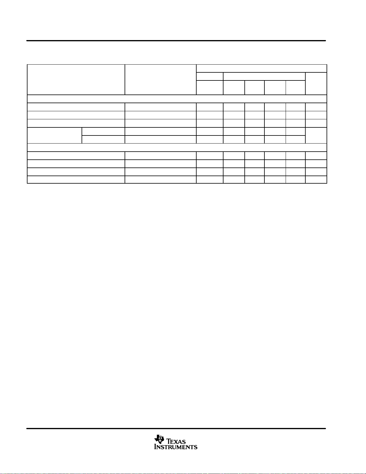
PARAMETER
TEST CONDITIONS
d
d
SLOS388B – OCTOBER 2001 – REVISED JUNE 2002
THS4601
electrical specifications: VS = ±5 V: RF = 250 Ω, RL = 1 kΩ and G = +2 (unless otherwise noted)
THS4601
TYP OVER TEMPERATURE
UNIT
dBc
dBc
mA
2.7 to
–2.0
2.6 to
–3.3
0°C to
70°C
2.6 to
–1.9
2.5 to
–3.2
25°C 25°C
AC PERFORMANCE
G = +1, VO = 20 mV
Small-signal bandwidth
Gain-bandwidth product G > +10 180 Typ MHz
Bandwidth for 0.1 dB flatness G = +2, VO = 200 mV
Large-signal bandwidth G = +5, VO = 5 V
Slew rate, SR G = +5, 5 V Step 100 Typ V/µs
Rise/fall time, tr/t
Settling time, t
Harmonic distortion G = +2, f = 1 MHz, VO = 2V
n
2
r
3
Harmonic
Input voltage noise, V
Input current noise, I
Differential gain (NTSC and P AL) G = +2, RL = 150 Ω 0.02% Typ
Differential phase (NTSC and P AL) G = +2, RL = 150 Ω 0.08 Typ _
DC PERFORMANCE
Open-loop voltage gain G = –10, RL = 1 kΩ 105 94 92 90 Min dB
Input offset voltage, V
Average offset voltage drift VCM = 0 V ±10 ±10 Typ µV/_C
Input bias current, I
Average bias current drift VCM = 0 V 50 50 Typ pA/°C
Input offset current, I
Average offset current drift VCM = 0 V 5 5 Typ pA/°C
INPUT
Common-mode input range, V
Common-mode rejection ratio, CMRR 110 100 95 90 Min dB
Input impedance, ZidDifferential 109 || 3.5 Typ Ω || pF
Input impedance, ZicCommon-mode 109 || 6.5 Typ Ω || pF
OUTPUT
Voltage output swing RL = 1 kΩ
Current output, I
Closed-loop output impedance, Z
s
Harmonic
O
f
0.01% G = +5, VO = 2 V Step 140 Typ ns
0.1% G = +5, VO = 2 V Step 170 Typ ns
n
n
IO
IB
IO
IC
Sourcing
Sinking
o
G = +2, VO = 40 mV
G = +5, VO = 100 mV
G = +10, VO = 200 mV
1.0 V Step 8 Typ ns
RL = 100 Ω –74 Typ
RL = 1 kΩ –84 Typ
RL = 100 Ω –79 Typ
RL = 1 kΩ –94 Typ
f > 10 kHz 5.4 Typ nV/√Hz
f > 10 kHz 5.5 Typ fA/√Hz
VCM = 0 V 1.0 4.0 4.5 5.0 Max mV
VCM = 0 V 20 100 550 1100 Max pA
VCM = 0 V 1 100 200 300 Max pA
RL = 20 Ω
G = +1, f = 1 MHz 0.1 Typ Ω
pp
pp
pp
pp
pp
pp
pp
400 Typ MHz
100 Typ MHz
50 Typ MHz
18 Typ MHz
5 Typ MHz
6 Typ MHz
±2.2
2.9 to
–3.5
–65 –48 –48 –47 Min
45 30 30 29 Min
–40°C
to 85°C
2.5 to
–1.8
2.3 to
–3.1
MIN/
MAX
Min V
Min V
www.ti.com
5
Page 6
THS4601
PARAMETER
TEST CONDITIONS
SLOS388B – OCTOBER 2001 – REVISED JUNE 2002
electrical specifications: VS = ±5 V; RF = 250 Ω, RL = 1 kΩ and G = +2 (unless otherwise noted)
(continued)
THS4601
TYP OVER TEMPERATURE
25°C 25°C
POWER SUPPLY
Specified operating voltage ±5 ±16.5 ±16.5 ±16.5 Max V
Maximum quiescent current 9.6 11.2 11.4 11.7 Max mA
Minimum quiescent current 9.6 8.2 8.0 7.7 Min mA
Power supply rejection
TEMPERATURE
Specified operating range, T
Thermal resistance, θ
8D: SO–8 170 Typ °C/W
8DDA: SO–8 with PowerPAD 67 Typ °C/W
+PSRR 110 90 88 86 Min
–PSRR 110 90 88 86 Min
–40 to 85 Typ °C
JA
A
Junction-to-ambient
0°C to
70°C
–40°C
to 85°C
MIN/
MAX
UNIT
dB
6
www.ti.com
Page 7

SLOS388B – OCTOBER 2001 – REVISED JUNE 2002
THS4601
TYPICAL CHARACTERISTICS
Table of Graphs
FIGURE
Small-Signal Unity Gain Frequency Response 2
Large-Signal Unity Gain Frequency Response 3
Small-Signal Frequency Response, Gain = +2 4
Small-Signal Frequency Response, Gain = +5 5
Small-Signal Frequency Response, Gain = +10 6
Small-Signal Frequency Response, Gain = +100 7
Open-Loop Gain and Phase vs Frequency 8
Voltage Noise vs Frequency 9
Rejection Ratios vs Frequency 10
Closed-Loop Output Impedance vs Frequency 11
Large-Signal Pulse Response 12
Harmonic Distortion vs Frequency 13
Harmonic Distortion vs Output Voltage Swing 14
Slew Rate vs Output Voltage Step 15
Input Bias Current vs Input Common-Mode Range 16
Common-Mode Rejection Ratio vs Input Common-Mode Range 17
Open-Loop Gain vs Temperature 18
Input Bias Current vs Temperature 19
Input Offset Current vs Temperature 20
Offset Voltage vs Temperature 21
Quiescent Current vs Temperature 22
Output Current vs Temperature 23
Output Voltage Swing vs Temperature 24
Rejection Ratios vs Temperature 25
www.ti.com
7
Page 8
THS4601
SLOS388B – OCTOBER 2001 – REVISED JUNE 2002
TYPICAL CHARACTERISTICS
measurement conditions: T
SMALL-SIGNAL UNITY GAIN
FREQUENCY RESPONSE
8
Gain = 1,
6
RF = 0Ω,
RL = 1 kΩ,
4
PIN = –30 dBm
2
0
Gain – dB
–2
–4
–6
–8
100 k 1 M 10 M 100 M 1 G
SMALL-SIGNAL FREQUENCY RESPONSE,
10
8
6
4
2
0
Gain – dB
–2
–4
Gain = 2,
–6
RF = 62Ω,
RL = 1 kΩ,
–8
PIN = –30 dBm
–10
100 k 1 M 10 M 100 M 1 G
Frequency – Hz
Figure 2
GAIN = +2
Frequency – Hz
Figure 4
= 25°C, RL = 1 kΩ, VS = ±15 V (unless otherwise noted)
A
LARGE-SIGNAL UNITY GAIN
FREQUENCY RESPONSE
5
0
–5
–10
Gain – dB
–15
Gain = 1,
RF = 0 Ω,
–20
RL = 1 kΩ,
PIN = 0 dBm
–25
100 k 1 M 10 M 100 M
Frequency – Hz
Figure 3
SMALL-SIGNAL FREQUENCY RESPONSE,
20
15
10
5
0
Gain – dB
–5
Gain = 5,
RF = 500Ω,
–10
RL = 1 kΩ,
PIN = –30 dBm
–15
100 k 1 M 10 M 100 M 1 G
GAIN = +5
Frequency – Hz
Figure 5
SMALL-SIGNAL FREQUENCY RESPONSE,
GAIN = +10
25
20
15
10
5
Gain – dB
0
Gain = 10,
–5
RF = 1 kΩ,
RL = 1 kΩ,
–10
PIN = –30 dBm
–15
100 k 1 M 10 M 100 M 1 G
Frequency – Hz
Figure 6
8
www.ti.com
SMALL-SIGNAL FREQUENCY RESPONSE,
GAIN = +100
50
Gain = 100,
40
30
20
Gain – dB
10
0
–10
100 k 1 M 10 M 100 M 1 G
Frequency – Hz
RF = 5 kΩ,
RL = 1 kΩ,
PIN = –30 dBm
Figure 7
Page 9
THS4601
SLOS388B – OCTOBER 2001 – REVISED JUNE 2002
TYPICAL CHARACTERISTICS
measurement conditions: T
OPEN-LOOP GAIN AND PHASE
110
100
90
80
70
60
50
40
Gain – dB
30
20
10
0
–10
10 100 1 k 10 k 100 k 1 M 10 M 100 M 1 G
REJECTION RATIOS
120
CMRR
100
80
PSRR–
vs
FREQUENCY
Frequency – Hz
Figure 8
vs
FREQUENCY
PSRR+
= 25°C, RL = 1 kΩ, VS = ±15 V (unless otherwise noted)
A
VOLTAGE NOISE
vs
90
60
30
0
–30
–60
–90
–120
–150
–180
–210
–240
–270
60
50
40
nV/ Hz
Phase – °
30
20
Voltage Noise –
10
0
10 100 1 k 10 k 100 k
FREQUENCY
Frequency – Hz
Figure 9
CLOSED-LOOP OUTPUT IMPEDANCE
vs
FREQUENCY
100
10
Ω
60
40
Rejection Ratio – dB
20
0
100 1 k 10 k 100 k 1 M
Frequency – Hz
Figure 10
LARGE-SIGNAL PULSE RESPONSE
3
2
1
0
–1
Output Voltage – V
–2
–3
0 0.2 0.4 0.6 0.8 1
t – Time – µs
Figure 12
10 M 100 M
1
Output Impedance –
0.1
0.01
100 k 1 M 10 M 100 M
Frequency – Hz
Figure 11
HARMONIC DISTORTION
vs
Gain = 2,
RF = 250 Ω,
RL = 1 kΩ,
VO = 2 V
PP
FREQUENCY
3rd Harmonic
2nd Harmonic
Frequency – Hz
–20
–30
–40
–50
–60
–70
Distortion – dBc
–80
–90
–100
100 k 1 M 10 M
Figure 13
www.ti.com
9
Page 10

THS4601
SLOS388B – OCTOBER 2001 – REVISED JUNE 2002
TYPICAL CHARACTERISTICS
measurement conditions: T
HARMONIC DISTORTION
OUTPUT VOLTAGE SWING
–50
–55
3rd Harmonic
–60
–65
–70
–75
–80
Distortion – dBc
–85
–90
–95
–100
024681012
Peak-to-Peak Output Swing – V
INPUT BIAS CURRENT
INPUT COMMON-MODE RANGE
10 k
1 k
vs
Figure 14
vs
= 25°C, RL = 1 kΩ, VS = ±15 V (unless otherwise noted)
A
SLEW RATE
vs
OUTPUT VOLTAGE STEP
130
2nd Harmonic
Gain = 2,
RF = 250 Ω,
RL = 1 kΩ,
f = 1 MHz
120
sµ
110
V/
100
90
Slew Rate –
80
70
60
0 5 10 15 20
SR–
SR+
Gain = 5,
RL = 1 kΩ
Output Voltage Step – V
Figure 15
COMMON-MODE REJECTION RATIO
vs
INPUT COMMON-MODE RANGE
120
100
60
100
10
Input Bias Current – pA
1
–15 –10 –5051015
Input Common-Mode Range – V
Figure 16
OPEN-LOOP GAIN
vs
TEMPERATURE
110
108
106
104
102
100
98
Open-Loop Gain – dB
96
94
92
–40 –20 0 20 40 60 80 100 120
Case Temperature – °C
Figure 18
80
CMRR – dB
40
20
0
–15 –10 –50 5 1015
Input Common-Mode Range – V
Figure 17
INPUT BIAS CURRENT
vs
100 k
10 k
1 k
100
Input Bias Current – pA
10
1
–40 –20 0 20 40 60 80 100 120
TEMPERATURE
IIB+
IIB–
Case Temperature – °C
Figure 19
10
www.ti.com
Page 11

THS4601
SLOS388B – OCTOBER 2001 – REVISED JUNE 2002
TYPICAL CHARACTERISTICS
measurement conditions: T
INPUT OFFSET CURRENT
15
10
5
0
–5
–10
–15
–20
–25
Input Offset Current – pA
–30
–35
–40
–40 –20 0 20 40 60 80 100 120
QUIESCENT CURRENT
10.2
10
9.8
9.6
9.4
Quiescent Current – mA
9.2
9
–40 –20 0 20 40 60 80 100 120
vs
TEMPERATURE
Case Temperature – °C
Figure 20
vs
TEMPERATURE
Case Temperature – °C
Figure 22
= 25°C, RL = 1 kΩ, VS = ±15 V (unless otherwise noted)
A
OFFSET VOLTAGE
vs
2.50
2
1.50
1
Offset Voltage – mV
0.50
0
–40 –20 0 20 40 60 80 100 120
TEMPERATURE
Case Temperature – °C
Figure 21
OUTPUT CURRENT
vs
90
85
80
75
70
65
60
55
Output Current – mA
50
45
40
–40 –20 0 20 40 60 80 100 120
TEMPERATURE
Sourcing Current
Sinking Current
Case Temperature – °C
Figure 23
OUTPUT VOLTAGE SWING
vs
TEMPERATURE
14
13.8
13.6
13.4
13.2
13
12.8
Positive Output Voltage Sling – V
12.6
12.4
–40 –20 0 20 40 60 80 100 120
Case Temperature – °C
VO–
VO+
Figure 24
–14
–13.8
–13.6
–13.4
–13.2
–13
–12.8
–12.6
–12.4
Negative Output Voltage Swing – V
www.ti.com
REJECTION RATIOS
vs
TEMPERATURE
130
125
120
CMRR
115
110
105
100
PSRR–
95
90
Rejection Ratios – dB
85
80
75
70
–40 –20 0 20 40 60 80 100 120
Case Temperature – °C
PSRR+
Figure 25
11
Page 12

THS4601
SLOS388B – OCTOBER 2001 – REVISED JUNE 2002
APPLICATION INFORMATION
introduction
The THS4601 is a high-speed, FET-input operational amplifier. The combination of its high frequency
capabilities and its DC precision make it a design option for a wide variety of applications, including test and
measurement, optical monitoring, transimpedance gain circuits, and high-impedance buffers. The applications
section of the data sheet discusses these particular applications in addition to general information about the
device and its features.
transimpedance fundamentals
FET-input amplifiers are often used in transimpedance applications because of their extremely high input
impedance. A transimpedance block accepts a current as an input and converts this current to a voltage at the
output. The high-input impedance associated with FET-input amplifiers minimizes errors in this process caused
by the input bias currents, I
designing the transimpedance circuit
Typically, design of a transimpedance circuit is driven by the characteristics of the current source that provides
the input to the gain block. A photodiode is the most common example of a capacitive current source that would
interface with a transimpedance gain block. Continuing with the photodiode example, the system designer
traditionally chooses a photodiode based on two opposing criteria: speed and sensitivity. Faster photodiodes
cause a need for faster gain stages, and more sensitive photodiodes require higher gains in order to develop
appreciable signal levels at the output of the gain stage.
, of the amplifier.
IB
These parameters affect the design of the transimpedance circuit in a few ways. First, the speed of the
photodiode signal determines the required bandwidth of the gain circuit. However, the required gain, based on
the sensitivity of the photodiode, limits the bandwidth of the circuit. Additionally, the larger capacitance
associated with a more sensitive signal source also detracts from the achievable speed of the gain block. The
dynamic range of the input signal also places requirements on the amplifier’s dynamic range. Knowledge of the
source’s output current levels, coupled with a desired voltage swing on the output, dictates the value of the
feedback resistor, R
. The transfer function from input to output is V
F
OUT
= IINRF.
The large gain-bandwidth product of the THS4601 provides the capability for achieving both high transimpedance gain and wide bandwidth simultaneously. In addition, the high power supply rails provide the
potential for a very wide dynamic range at the output, allowing for the use of input sources which possess wide
dynamic range. The combination of these characteristics makes the THS4601 a design option for systems that
require transimpedance amplification of wideband, low-level input signals. A standard transimpedance circuit
is shown in Figure 26.
C
F
R
F
λ
–V
Bias
_
+
R
L
Figure 26. Wideband Photodiode Transimpedance Amplifier
12
www.ti.com
Page 13

SLOS388B – OCTOBER 2001 – REVISED JUNE 2002
APPLICATION INFORMATION
designing the transimpedance circuit (continued)
As indicated, the current source typically sets the requirements for gain, speed, and dynamic range of the
amplifier. For a given amplifier and source combination, achievable performance is dictated by the following
parameters: the amplifier’s gain-bandwidth product, the amplifier’s input capacitance, the source capacitance,
the transimpedance gain, the amplifier’s slew rate, and the amplifier’s output swing. From this information, the
optimal performance of a transimpedance circuit using a given amplifier can be determined. Optimal is defined
here as providing the required transimpedance gain with a maximally flat frequency response.
For the circuit shown in Figure 26, all but one of the design parameters is known; the feedback capacitor must
be determined. Proper selection of the feedback capacitor prevents an unstable design, controls pulse
response characteristics, provides maximally flat transimpedance bandwidth, and limits broadband integrated
noise. The maximally flat frequency response results with C
the feedback capacitor, R
capacitance and parasitic capacitance at the inverting node), and GBP is the gain-bandwidth product of the
amplifier in hertz.
1
pRFGBP
)
Ǹ
is the feedback resistor, CS is the total source capacitance (including amplifier input
F
2
4C
1
ǒ
pRFGBP
Ǔ
)
S
pRFGBP
calculated as shown in equation 1, where CF is
F
THS4601
(1)
C
+
F
Once the optimal feedback capacitor has been selected, the transimpedance bandwidth can be calculated with
equation 2.
F
C
I
DIODE
NOTE: The total source capacitance is the sum of several distinct capacitances.
–3dB
ICM
+
Ǹ
C
IDIFF
C
P
C
D
2pR
2
GBP
ǒ
CS) C
F
+
_
R
C
Figure 27. Transimpedance Analysis Circuit
Ǔ
F
Cs = C
Where: C
F
F
ICM
+ C
IDIFF
is the common-mode input capacitance.
ICM
is the differential input capacitance.
C
IDIFF
is the diode capacitance.
C
D
is parasitic capacitance at the inverting node.
C
P
+ CP + C
D
(2)
www.ti.com
13
Page 14

THS4601
SLOS388B – OCTOBER 2001 – REVISED JUNE 2002
APPLICATION INFORMATION
designing the transimpedance circuit (continued)
The feedback capacitor provides a pole in the noise gain of the circuit, counteracting the zero in the noise gain
caused by the source capacitance. The pole is set such that the noise gain achieves a 20 dB per decade
rate-of-closure with the open-loop gain response of the amplifier, resulting in a stable circuit. As indicated, the
formula given provides the feedback capacitance for maximally flat bandwidth. Reduction in the value of the
feedback capacitor can increase the signal bandwidth, but this occurs at the expense of peaking in the AC
response.
A
Gain
OL
–20 dB/
Decade
Noise Gain
20 dB/
Decade
0
Zero Pole
20 dB/Decade
Rate-of-Closure
GBP
f
Figure 28. Transimpedance Circuit Bode Plot
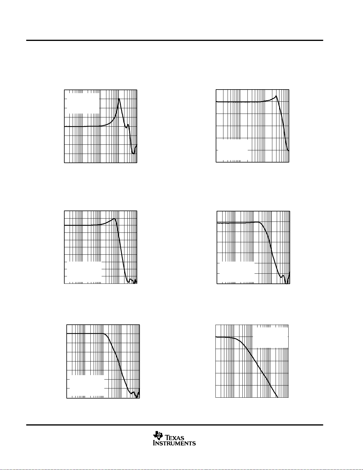
The performance of the THS4601 has been measured for a variety of transimpedance gains with a variety of
source capacitances. The achievable bandwidths of the various circuit configurations are summarized
numerically in the table. The frequency responses are presented in the Figures 27, 28, and 29.
Note that the feedback capacitances do not correspond exactly with the values predicted by the equation. They
have been tuned to account for the parasitic capacitance of the feedback resistor (typically 0.2 pF for 0805
surface mount devices) as well as the additional capacitance associated with the PC board. The equation
should be used as a starting point for the design, with final values for C
optimized in the laboratory.
F
14
www.ti.com
Page 15

APPLICATION INFORMATION
designing the transimpedance circuit (continued)
T able 1. Transimpedance Performance Summary for Various Configurations
THS4601
SLOS388B – OCTOBER 2001 – REVISED JUNE 2002
SOURCE CAPACITANCE
TRANSIMPEDANCE GAIN
(pF)
18 10k 2.2 10.4
18 100k 0.6 3.3
18 1M 0 1.1
47 10k 3.3 7.6
47 100k 0.6 2.8
47 1M 0 0.88
100 10k 3.9 5.9
100 100k 1.5 1.3
100 1M 0 0.62
220 10k 5.6 3.8
220 100k 1.8 1.1
220 1M 0.4 0.36
10 kΩ TRANSIMPEDANCE BANDWIDTH
FOR VARIOUS SOURCE CAPACITANCES
90
85
CS = 18 pF, CF = 2.2 pF
80
CS = 47 pF,
75
Transimpedance Gain – dB
70
65
10 k 100 k 1 M 10 M 100 M
CF = 3.3 pF
CS = 100 pF,
CF = 3.9 pF
CS = 220 pF,
CF = 5.6 pF
Frequency – Hz
Figure 29
(Ω)
FEEDBACK CAPACITANCE
100 kΩ TRANSIMPEDANCE BANDWIDTH
FOR VARIOUS SOURCE CAPACITANCES
105
100
95
90
85
80
75
70
Transimpedance Gain – dB
65
60
10 k 100 k 1 M 10 M
CS = 18 pF,
CF = 0.6 pF
CS = 47 pF,
CF = 0.6 pF
CS = 100 pF,
CF = 1.5 pF
CS = 220 pF,
CF = 1.8 pF
Frequency – Hz
Figure 30
(pF)
(MHz)
1 MΩ TRANSIMPEDANCE BANDWIDTH
FOR VARIOUS SOURCE CAPACITANCES
–3 dB FREQUENCY
130
125
120
CS = 47 pF,
CS = 100 pF,
CS = 220 pF,
10 k 100 k 1 M 10 M
Transimpedance Gain – dB
115
110
105
100
95
90
CS = 18 pF, CF = 0
CF = 0
CF = 0
CF = 0.4 pF
Frequency – Hz
Figure 31
measuring transimpedance bandwidth
While there is no substitute for measuring the performance of a particular circuit under the exact conditions that
are used in the application, the complete system environment often makes measurements harder. For
transimpedance circuits, it is difficult to measure the frequency response with traditional laboratory equipment
because the circuit requires a current as an input rather than a voltage. Also, the capacitance of the current
source has a direct effect on the frequency response. A simple interface circuit can be used to emulate a
capacitive current source with a network analyzer. With this circuit, transimpedance bandwidth measurements
are simplified, making amplifier evaluation easier and faster.
www.ti.com
15
Page 16

THS4601
SLOS388B – OCTOBER 2001 – REVISED JUNE 2002
APPLICATION INFORMATION
measuring transimpedance bandwidth (continued)
I
Network Analyzer
50 Ω 50 Ω
R
S
V
S
NOTE: This interface network creates a capacitive, constant current source from a network analyzer and properly terminates the network analyzer
at high frequencies.
Figure 32. Emulating a Capacitive Current Source With a Network Analyzer
The transconductance transfer function of the interface circuit is
s
C
1
1)
2R
V
I
O
s
(s) +
s)
S
2R
ǒ
S
Ǔ
C
2
1
ǒ
C
) C
1
O
C
2
C
1
.
Ǔ
2
I
O
+
V
S
2R
1
ǒ
1)
S
(above the pole frequency)
C
1
Ǔ
C
2
This transfer function contains a zero at DC and a pole at
1
constant at
also properly terminates the network analyzer with 50 Ω at high frequencies. The second requirement for this
current source is to provide the desired output impedance, emulating the output impedance of a photodiode or
other current source. The output impedance of this circuit is given by
ZO(s) +
Assuming C1 >> C2, the equation reduces to
frequency.
Capacitor values should be chosen to satisfy two requirements. First, C2 should represent the anticipated
capacitance of the true source. C
transconductance network is much less than the transimpedance bandwidth of the circuit. Choosing this corner
frequency properly leads to more accurate measurements of the transimpedance bandwidth. If the interface
circuit’s corner frequency is too close to the bandwidth of the circuit, determining the power level in the flatband
is difficult. A decade or more of flat bandwidth provides a good basis for determining the proper transimpedance
bandwidth.
2R
S
C
ǒ
1)
) C
1
C1C
, above the pole frequency , providing a controllable AC current source. This circuit
C
1
Ǔ
C
2
2R
1
ǒ
C
s
1
2R
ȳ
Ǔ
) C
2
ȧ
.
ȧ
ȧ
1
Ǔ
C
s
ȴ
1
1
[
Z
O
sC
should then be chosen such that the corner frequency of the
1
ȱ
s)
ȧ
2
ȧ
ȧ
2
sǒs)
Ȳ
s +
2R
giving the appearance of a capacitive source at higher
,
2
1
ǒ
C
1
S
. The transconductance is
Ǔ
C
)
2
16
www.ti.com
Page 17

SLOS388B – OCTOBER 2001 – REVISED JUNE 2002
APPLICATION INFORMATION
alternative transimpedance configurations
Other transimpedance configurations are possible. Three possibilities are shown below.
The first configuration is a slight modification of the basic transimpedance circuit. By splitting the feedback
resistor, the feedback capacitor value becomes more manageable and easier to control. This type of
compensation scheme is useful when the feedback capacitor required in the basic configuration becomes so
small that the parasitic effects of the board and components begin to dominate the total feedback capacitance.
By reducing the resistance across the capacitor, the capacitor value can be increased. This mitigates the
dominance of the parasitic effects.
C
F
THS4601
R
F1
λ
–V
Bias
NOTE: Splitting the feedback resistor enables use of a larger, more manageable feedback
capacitor.
R
F2
_
+
R
L
Figure 33. Alternative Transimpedance Configuration #1
The second configuration uses a resistive T-network to achieve very high transimpedance gains using relatively
small resistor values. This topology can be very useful when the desired transimpedance gain exceeds the
value of available resistors. The transimpedance gain is given by equation 3.
R
1 )
F2
Ǔ
R
F3
C
R
F3
R
F1
λ
F
R
F2
_
+
R
L
(3)
R
+ R
EQ
F1
ǒ
–V
Bias
NOTE: A resistive T-network enables high transimpedance gain with reasonable resistor values.
Figure 34. Alternative Transimpedance Configuration #2
www.ti.com
17
Page 18

THS4601
SLOS388B – OCTOBER 2001 – REVISED JUNE 2002
APPLICATION INFORMATION
alternative transimpedance configurations (continued)
The third configuration uses a capacitive T-network to achieve fine control of the compensation capacitance.
The capacitor C
behaves the same as the basic transimpedance configuration, with the effective C
1
+
C
FEQ
can be used to tune the total effective feedback capacitance to a very fine degree. This circuit
F3
C
1 )
F3
Ǔ
C
F2
C
F3
1
ǒ
C
F1
given by equation 4.
F
(4)
C
F1
λ
–V
Bias
NOTE: A capacitive T-network enables fine control of the effective
feedback capacitance using relatively large capacitor values.
C
F2
R
F
_
+
R
L
Figure 35. Alternative Transimpedance Configuration #3
summary of key decisions in transimpedance design
The following is a quick, simplified process for basic transimpedance circuit design. This process gives a quick
start to the design process, though it does ignore some aspects that may be critical to the circuit.
Step 1: Determine the capacitance of the source.
Step 2: Calculate the total source capacitance, including the amplifier input capacitance, C
Step 3: Determine the magnitude of the possible current output from the source, including the minimum
signal current anticipated and maximum signal current anticipated.
ICM
and C
IDIFF
.
Step 4: Choose a feedback resistor value such that the input current levels create the desired output signal
voltages, and ensure that the output voltages can accommodate the dynamic range of the input
signal.
Step 5: Calculate the optimum feedback capacitance using equation 1.
Step 6: Calculate the bandwidth given the resulting component values.
Step 7: Evaluate the circuit to see if all design goals are satisfied.
18
www.ti.com
Page 19

SLOS388B – OCTOBER 2001 – REVISED JUNE 2002
APPLICATION INFORMATION
selection of feedback resistors
Feedback resistor selection can have a significant effect on the performance of the THS4601 in a given
application, especially in configurations with low closed-loop gain. If the amplifier is configured for unity gain,
the output should be directly connected to the inverting input. Any resistance between these two points interacts
with the input capacitance of the amplifier and causes an additional pole in the frequency response. For
non-unity gain configurations, low resistances are desirable for flat frequency response. However, care must
be taken not to load the amplifier too heavily with the feedback network if large output signals are expected. In
most cases, a tradeoff will be made between the frequency response characteristics and the loading of the
amplifier. For a gain of 2, a 250 Ω feedback resistor is a suitable operating point from both perspectives.
If resistor values are chosen too large, the THS4601 is subject to oscillation problems. For example, an inverting
amplifier configuration with a 1-kΩ gain resistor and a 1-kΩ feedback resistor develops an oscillation due to the
interaction of the large resistors with the input capacitance. In low gain configurations, avoid feedback resistors
this large or anticipate using an external compensation scheme to stabilize the circuit.
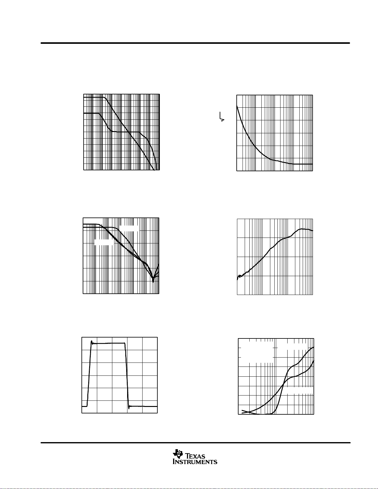
overdrive recovery
The THS4601 has an overdrive recovery period when the output is driven close to one power supply rail or the
other. The overdrive recovery time period is dependent upon the magnitude of the overdrive and whether the
output is driven towards the positive or the negative power supply. The four graphs shown here depict the
overdrive recovery time in two cases, an attempted 28 V
on the output. Note that in both of these cases, the output does not achieve these levels as the output voltage
swing is limited to less than these values, but these values are representative of the desired signal swing on
the output for the given inputs. As shown in the figures, the recovery period increases as the magnitude of the
overdrive increases, with the worst case recovery occurring with the negative rail. The recovery times are
summarized in Table 2.
signal on the output and an attempted 30 VPP signal
PP
THS4601
T able 2. Overdrive Recovery Characteristics
VOLTAGE RAIL
+V
S
–V
S
+V
S
–V
S
IDEAL OUTPUT SWING
(VPP)
28 320
28 340
30 540
30 680
OVERDRIVE RECOVERY TIME
(ns)
www.ti.com
19
Page 20

THS4601
SLOS388B – OCTOBER 2001 – REVISED JUNE 2002
overdrive recovery (continued)
APPLICATION INFORMATION
RISING EDGE OVERDRIVE RECOVERY
20
Gain = 5,
VIN = 5.57 VPP,
15
Recovery Time = 340 ns
10
5
0
–5
Output Voltage – V
–10
–15
–20
01234
Input
Time – µs
Output
Figure 36
RISING EDGE OVERDRIVE RECOVERY
20
Gain = 5,
VIN = 6 VPP,
15
Recovery Time = 680 ns
10
5
0
–5
Output Voltage – V
–10
–15
–20
01234
Input
Output
Time – µs
Figure 38
FALLING EDGE OVERDRIVE RECOVERY
4
3
2
1
0
–1
Input Voltage – V
–2
–3
–4
20
15
10
5
0
–5
Output Voltage – V
–10
Gain = 5,
–15
VIN = 5.57 VPP,
Recovery Time = 320 ns
–20
01234
Output
Input
Time – µs
4
3
2
1
0
–1
Input Voltage – V
–2
–3
–4
Figure 37
FALLING EDGE OVERDRIVE RECOVERY
4
3
2
1
0
–1
Input Voltage – V
–2
–3
–4
20
15
10
5
0
–5
Output Voltage – V
–10
–15
–20
01234
Input
Gain = 5,
VIN = 6 VPP,
Recovery Time = 540 ns
Output
Time – µs
4
3
2
1
0
–1
Input Voltage – V
–2
–3
–4
Figure 39
high frequency continuous wave amplification
When presented with high frequency sinusoids in low-gain configurations (G < 5), the THS4601 experiences
a relatively large differential input voltage between the two input terminals of the amplifier. As this differential
input voltage increases, the internal slew-boosting circuitry can cause some transistors in the signal path to
enter the cutoff region of operation. As the derivative of the signal changes signs, these transistors suffer from
a short recovery time period, generating appreciable levels of distortion. This behavior is depicted in the graph
Harmonic Distortion vs Frequency . At 2 MHz with a 2 V
output signal, the distortion rises significantly . For most
PP
high-gain configurations including transimpedance applications, this phenomena is not problematic.
slew rate performance with varying input step amplitude and rise/fall time
Some FET input amplifiers exhibit the peculiar behavior of having a larger slew rate when presented with smaller
input voltage steps and slower edge rates due to a change in bias conditions in the input stage of the amplifier
under these circumstances. This phenomena is most commonly seen when FET input amplifiers are used as
voltage followers. As this behavior is typically undesirable, the THS4601 has been designed to avoid these
issues. Larger amplitudes lead to higher slew rates, as would be anticipated, and fast edges do not degrade
the slew rate of the device.
20
www.ti.com
Page 21

SLOS388B – OCTOBER 2001 – REVISED JUNE 2002
APPLICATION INFORMATION
power dissipation and thermal characteristics
The THS4601 does not incorporate automatic thermal shutoff protection, so the designer must take care to
ensure that the design does not violate the absolute maximum junction temperature of the device. Failure may
result if the absolute maximum junction temperature of 150°C is exceeded.
The thermal characteristics of the device are dictated by the package and the PC board. Maximum power
dissipation for a given package can be calculated using the following formula.
T
–T
max
A
q
JA
Where:
P
Dmax
+
THS4601
P
T
T
θ
is the maximum power dissipation (W)
Dmax
is the absolute maximum junction temperature (°C)
max
is the ambient temperature (°C)
A
is the thermal coefficient from the silicon junctions to the ambient air (°C/W)
JA
For systems where heat dissipation is more critical, the THS4601 is offered in an 8-pin SOIC with PowerP AD.
The thermal coefficient for the SOIC PowerP AD is substantially improved over the traditional SOIC. Maximum
power dissipation levels are depicted in the graph for the two packages. The data for the 8DDA package
assumes a board layout that follows the PowerPAD layout guidelines.
MAXIMUM POWER DISSIPATION
3
2.5
2
8DDA Package
1.5
1
8D Package
0.5
Maximum Power Dissipation – W
0
–40 –20 0 20406080
Ambient Temperature – °C
vs
TEMPERATURE
θJA = 170°C/W for 8D,
θJA = 66.6°C/W for 8DDA
Figure 40
When determining whether or not the device satisfies the maximum power dissipation requirement, it is
important to not only consider quiescent power dissipation, but also dynamic power dissipation. Often times,
this is difficult to quantify because the signal pattern is inconsistent, but an estimate of the RMS power
dissipation can provide visibility into a possible problem.
www.ti.com
21
Page 22

THS4601
SLOS388B – OCTOBER 2001 – REVISED JUNE 2002
APPLICATION INFORMATION
PC board layout guidelines
Achieving optimum performance with a high frequency amplifier requires careful attention to board layout
parasitics and external component selection. Recommendations that optimize performance include the
following.
D Use of a ground plane—It is highly recommended that a ground plane be used on the board to provide all
components with a low impedance connection to ground. However, the ground plane should be cleared
around the amplifier inputs and outputs to minimize parasitic capacitance. A solid ground plane is
recommended wherever possible.
D Proper power supply decoupling—A 6.8 µF tantalum capacitor and a 0.1 µF ceramic capacitor should be
used on each power supply node. Good performance is possible if the 6.8 µF capacitor is shared among
several amplifiers, but each amplifier should have a dedicated 0.1 µF capacitor for each supply. The 0.1
µF capacitor should be placed as close to the power supply pins as possible. As the distance from the device
increases, the trace inductance rises and decreases the effectiveness of the capacitor . A good design has
less than 2.5 mm separating the ceramic capacitor and the power supply pin. The tantalum capacitors can
be placed significantly further away from the device.
D Avoid sockets—Sockets are not recommended for high-speed amplifiers. The lead inductance associated
with the socket pins often leads to stability problems. Direct soldering to a printed-circuit board yields the
best performance.
D Minimize trace length and place parts compactly—Shorter traces minimize stray parasitic elements of the
design and lead to better high-frequency performance.
D Use of surface mount passive components—Surface mount passive components are recommended due
to the extremely low lead inductance and the small component footprint. These characteristics minimize
problems with stray series inductance and allow for a more compact circuit layout. Compact layout reduces
both parasitic inductance and capacitance in the design.
D Minimize parasitic capacitance on the signal input and output pins—Parasitic capacitance on the input and
output pins can degrade high frequency behavior or cause instability in the circuit. Capacitance on the
inverting input or the output is a common cause of instability in high performance amplifiers, and
capacitance on the noninverting input can react with the source impedance to cause unintentional
band-limiting. To reduce unwanted capacitance around these pins, a window should be opened up in the
signal/power layers that are underneath those pins. Power and ground planes should otherwise be
unbroken.
PowerPAD design considerations
The THS4601 is available in a thermally-enhanced PowerP AD package. This package is constructed using a
downset leadframe upon which the die is mounted (see Figure 39). This arrangement results in the lead frame
exposed as a thermal pad on the underside of the package. Because this thermal pad has direct thermal contact
with the die, excellent thermal performance can be achieved by providing a good thermal path away from the
thermal pad.
The PowerP AD package allows for both assembly and thermal management in one manufacturing operation.
During the surface-mount solder operation (when the leads are being soldered), the thermal pad can also be
soldered to a copper area underneath the package. Through the use of thermal paths within this copper area,
heat can be conducted away from the package into either a ground plane or other heat dissipating device. The
PowerPAD is electrically insulated from the amplifier circuitry, but connection to the ground plane is
recommended due to the high thermal mass typically associated with a ground plane.
The PowerPAD package represents a breakthrough in combining the small area and ease of assembly of
surface mount with the, heretofore, awkward mechanical methods of heatsinking.
22
www.ti.com
Page 23

APPLICATION INFORMATION
PowerPAD design considerations (continued)
DIE
THS4601
SLOS388B – OCTOBER 2001 – REVISED JUNE 2002
Side View (a)
DIE
End View (b) Bottom View (c)
NOTE A: The thermal pad is electrically isolated from all terminals in the package.
Thermal
Pad
Figure 41. Views of Thermally Enhanced Package
Although there are many ways to properly heatsink the PowerPAD package, the following steps illustrate the
recommended approach.
Thermal pad area (68 mils x 70 mils) with 5 vias
(Via diameter = 13 mils)
Figure 42. PowerPAD PCB Etch and Via Pattern
PowerPAD PCB LAYOUT CONSIDERATIONS
1. Prepare the PCB with a top side etch pattern as shown in Figure 42. There should be etch for the leads as
well as etch for the thermal pad.
2. Place five vias in the area of the thermal pad. These holes should be 13 mils in diameter . Keep them small
so that solder wicking through the holes does not occur during reflow.
3. Additional vias may be placed anywhere along the thermal plane outside of the thermal pad area. This helps
dissipate the heat generated by the IC. These additional vias may be larger than the 13-mil diameter vias
directly under the thermal pad. Larger vias are permissible here because they are not susceptible to solder
wicking as the vias underneath the device.
4. Connect all vias to the internal ground plane for best thermal characteristics
5. When connecting these holes to the ground plane, do not use the typical web or spoke via connection
methodology . Web connections have a high thermal resistance connection that is useful for slowing the heat
transfer during soldering operations. This makes the soldering of vias that have plane connections easier.
In this application, however , low thermal resistance is desired for the most efficient heat transfer. Therefore,
the holes under the PowerP AD package should make their connection to the internal ground plane with a
complete connection around the entire circumference of the plated-through hole.
6. The top-side solder mask should leave the terminals of the package and the thermal pad area with its five
holes exposed. The bottom-side solder mask should cover the five holes of the thermal pad area. This
prevents solder from being pulled away from the thermal pad area during the reflow process.
7. Apply solder paste to the exposed thermal pad area and all of the IC terminals.
8. With these preparatory steps in place, the IC is simply placed in position and run through the solder reflow
operation as any standard surface-mount component. This results in a part that is properly installed.
www.ti.com
23
Page 24

THS4601
SLOS388B – OCTOBER 2001 – REVISED JUNE 2002
APPLICATION INFORMATION
evaluation module and applications support
An evaluation board is available for quick laboratory verification of performance. An evaluation module can be
ordered from T exas Instruments’ web site (www .ti.com) or from your local TI sales representative. Applications
support is also available for designers. The Product Information Center (PIC) can put designers in touch with
applications engineers at Texas Instruments. The PIC be contacted via the web site as well.
additional reference material
D PowerPAD Made Easy, application brief, Texas Instruments Literature Number SLMA004.
D PowerP AD Thermally Enhanced Package, technical brief, T exas Instruments Literature Number SLMA002.
D Noise Analysis of FET Transimpedance Amplifiers, application bulletin, Texas Instruments Literature
Number SBOA060.
D Tame Photodiodes With Op Amp Bootstrap, application bulletin, Texas Instruments Literature Number
SBBA002.
D Designing Photodiode Amplifier Circuits With OPA128, application bulletin, Texas Instruments Literature
Number SBOA061.
D Photodiode Monitoring With Op Amps, application bulletin, Texas Instruments Literature Number
SBOA035.
D Comparison of Noise Performance Between a FET T ransimpedance Amplifier and a Switched Integrator,
Application Bulletin, Texas Instruments Literature Number SBOA034.
24
www.ti.com
Page 25

SLOS388B – OCTOBER 2001 – REVISED JUNE 2002
THS4601
MECHANICAL DATA
D (R-PDSO-G**) PLASTIC SMALL-OUTLINE PACKAGE
8 PINS SHOWN
8 5
1 4
A
0.069 (1,75) MAX
0.020 (0,51)
0.014 (0,35)
0.157 (4,00)
0.150 (3,81)
0.010 (0,25)
0.004 (0,10)
0.244 (6,20)
0.228 (5,80)
0.010 (0,25)0.050 (1,27)
0.008 (0,20) NOM
Gage Plane
0.010 (0,25)
0°– 8°
0.044 (1,12)
0.016 (0,40)
Seating Plane
0.004 (0,10)
PINS **
DIM
A MAX
A MIN
NOTES: A. All linear dimensions are in inches (millimeters).
B. This drawing is subject to change without notice.
C. Body dimensions do not include mold flash or protrusion, not to exceed 0.006 (0,15).
D. Falls within JEDEC MS-012
8
0.197
(5,00)
0.189
(4,80)
14
0.344
(8,75)
0.337
(8,55)
16
0.394
(10,00)
0.386
(9,80)
4040047/E 09/01
www.ti.com
25
Page 26

THS4601
SLOS388B – OCTOBER 2001 – REVISED JUNE 2002
MECHANICAL DATA
DDA (S–PDSO–G8) Power P AD t PLASTIC SMALL-OUTLINE
1,27
85
14
4,98
4,80
0,49
0,35
3,99
3,81
1,68 MAX
M
0,10
6,20
5,84
Seating Plane
Thermal Pad
(See Note D)
0,20 NOM
0°–8°
Gage Plane
0,25
0,89
0,41
1,55
1,40
NOTES: A. All linear dimensions are in millimeters.
B. This drawing is subject to change without notice.
C. Body dimensions do not include mold flash or protrusion not to exceed 0,15.
D. The package thermal performance may be enhanced by bonding the thermal pad to an external thermal plane.
This pad is electrically and thermally connected to the backside of the die and possibly selected leads.
PowerPAD is a trademark of Texas Instruments.
0,13
0,03
0,10
4202561/A 02/01
26
www.ti.com
Page 27

IMPORTANT NOTICE
Texas Instruments Incorporated and its subsidiaries (TI) reserve the right to make corrections, modifications,
enhancements, improvements, and other changes to its products and services at any time and to discontinue
any product or service without notice. Customers should obtain the latest relevant information before placing
orders and should verify that such information is current and complete. All products are sold subject to TI’s terms
and conditions of sale supplied at the time of order acknowledgment.
TI warrants performance of its hardware products to the specifications applicable at the time of sale in
accordance with TI’s standard warranty . Testing and other quality control techniques are used to the extent TI
deems necessary to support this warranty . Except where mandated by government requirements, testing of all
parameters of each product is not necessarily performed.
TI assumes no liability for applications assistance or customer product design. Customers are responsible for
their products and applications using TI components. T o minimize the risks associated with customer products
and applications, customers should provide adequate design and operating safeguards.
TI does not warrant or represent that any license, either express or implied, is granted under any TI patent right,
copyright, mask work right, or other TI intellectual property right relating to any combination, machine, or process
in which TI products or services are used. Information published by TI regarding third–party products or services
does not constitute a license from TI to use such products or services or a warranty or endorsement thereof.
Use of such information may require a license from a third party under the patents or other intellectual property
of the third party , or a license from TI under the patents or other intellectual property of TI.
Reproduction of information in TI data books or data sheets is permissible only if reproduction is without
alteration and is accompanied by all associated warranties, conditions, limitations, and notices. Reproduction
of this information with alteration is an unfair and deceptive business practice. TI is not responsible or liable for
such altered documentation.
Resale of TI products or services with statements different from or beyond the parameters stated by TI for that
product or service voids all express and any implied warranties for the associated TI product or service and
is an unfair and deceptive business practice. TI is not responsible or liable for any such statements.
Mailing Address:
Texas Instruments
Post Office Box 655303
Dallas, Texas 75265
Copyright 2002, Texas Instruments Incorporated
 Loading...