

Datasheet THS10064CDAR, THS10064IDA, THS10064CDA, THS10064IDAR Datasheet (Texas Instruments)
Page 1
THS10064
10-BIT 6 MSPS, SIMULTANEOUS SAMPLING
ANALOG-TO-DIGITAL CONVERTER
SLAS255 – DECEMBER 1999
1
POST OFFICE BOX 655303 • DALLAS, TEXAS 75265
features
D
Simultaneous Sampling of 4 Single-Ended
Signals or 2 Differential Signals or
Combination of Both
D
Integrated 16-Word FIFO
D
Signal-to-Noise and Distortion Ratio: 59 dB
at f
I
= 2 MHz
D
Differential Nonlinearity Error: ±1 LSB
D
Integral Nonlinearity Error: ±1 LSB
D
Auto-Scan Mode for 2, 3, or 4 Inputs
D
3-V or 5-V Digital Interface Compatible
D
Low Power: 216 mW Max
D
5-V Analog Single Supply Operation
D
Internal Voltage References . . . 50 PPM/°C
and ±5% Accuracy
D
Parallel µC/DSP Interface
applications
D
Radar Applications
D
Communications
D
Control Applications
D
High-Speed DSP Front-End
D
Automotive Applications
description
The THS10064 is a CMOS, low-power, 10-bit,
6 MSPS analog-to-digital converter (ADC). The
speed, resolution, bandwidth, and single-supply
operation are suited for applications in radar,
imaging, high-speed acquisition, and
communications. A multistage pipelined
architecture with output error correction logic
provides for no missing codes over the full
operating temperature range. Internal control
registers are used to program the ADC into the desired mode. The THS10064 consists of four analog inputs,
which are sampled simultaneously . These inputs can be selected individually and configured to single-ended
or differential inputs. An integrated 16 word deep FIFO allows the storage of data in order to improve data
transfers to the processor. Internal reference voltages for the ADC (1.5 V and 3.5 V) are provided.
An external reference can also be chosen to suit the dc accuracy and temperature drift requirements of the
application. Two different conversion modes can be selected. In single conversion mode, a single and
simultaneous conversion of up to four inputs can be initiated by using the single conversion start signal
(CONVST
). The conversion clock in single conversion mode is generated internally using a clock oscillator
circuit. In continuous conversion mode, an external clock signal is applied to the CONV_CLK input of the
THS10064. The internal clock oscillator is switched off in continuous conversion mode.
The THS10064C is characterized for operation from 0°C to 70°C, and the THS10064I is characterized for
operation from –40°C to 85°C.
Copyright 1999, Texas Instruments Incorporated
PRODUCTION DATA information is current as of publication date.
Products conform to specifications per the terms of Texas Instruments
standard warranty. Production processing does not necessarily include
testing of all parameters.
Please be aware that an important notice concerning availability, standard warranty, and use in critical applications of
Texas Instruments semiconductor products and disclaimers thereto appears at the end of this data sheet.
1
2
3
4
5
6
7
8
9
10
11
12
13
14
15
16
32
31
30
29
28
27
26
25
24
23
22
21
20
19
18
17
D0
D1
D2
D3
D4
D5
BV
DD
BGND
D6
D7
D8
D9
RA0
RA1
CONV_CLK (CONVST
)
DATA_AV
AINP
AINM
BINP
BINM
REFIN
REFOUT
REFP
REFM
AGND
AV
DD
CS0
CS1
WR
(R/W)
RD
DV
DD
DGND
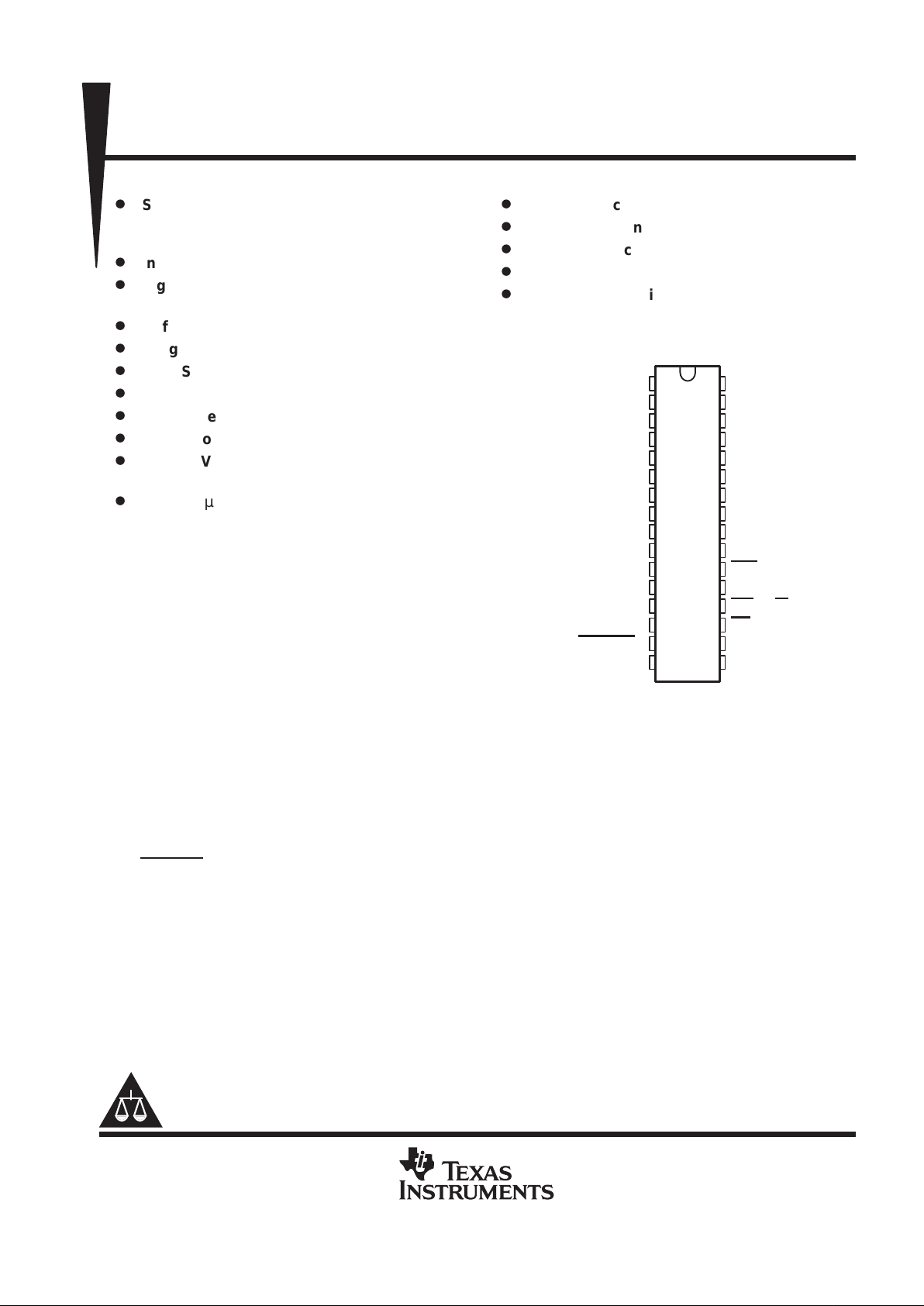
DA (TSSOP) PACKAGE
(TOP VIEW)
Page 2
THS10064
10-BIT 6 MSPS, SIMULTANEOUS SAMPLING
ANALOG-TO-DIGITAL CONVERTER
SLAS255 – DECEMBER 1999
2
POST OFFICE BOX 655303 • DALLAS, TEXAS 75265
AVAILABLE OPTIONS
PACKAGED DEVICE
T
A
TSSOP
(DA)
0°C to 70°C THS10064CDA
–40°C to 85°C THS10064IDA
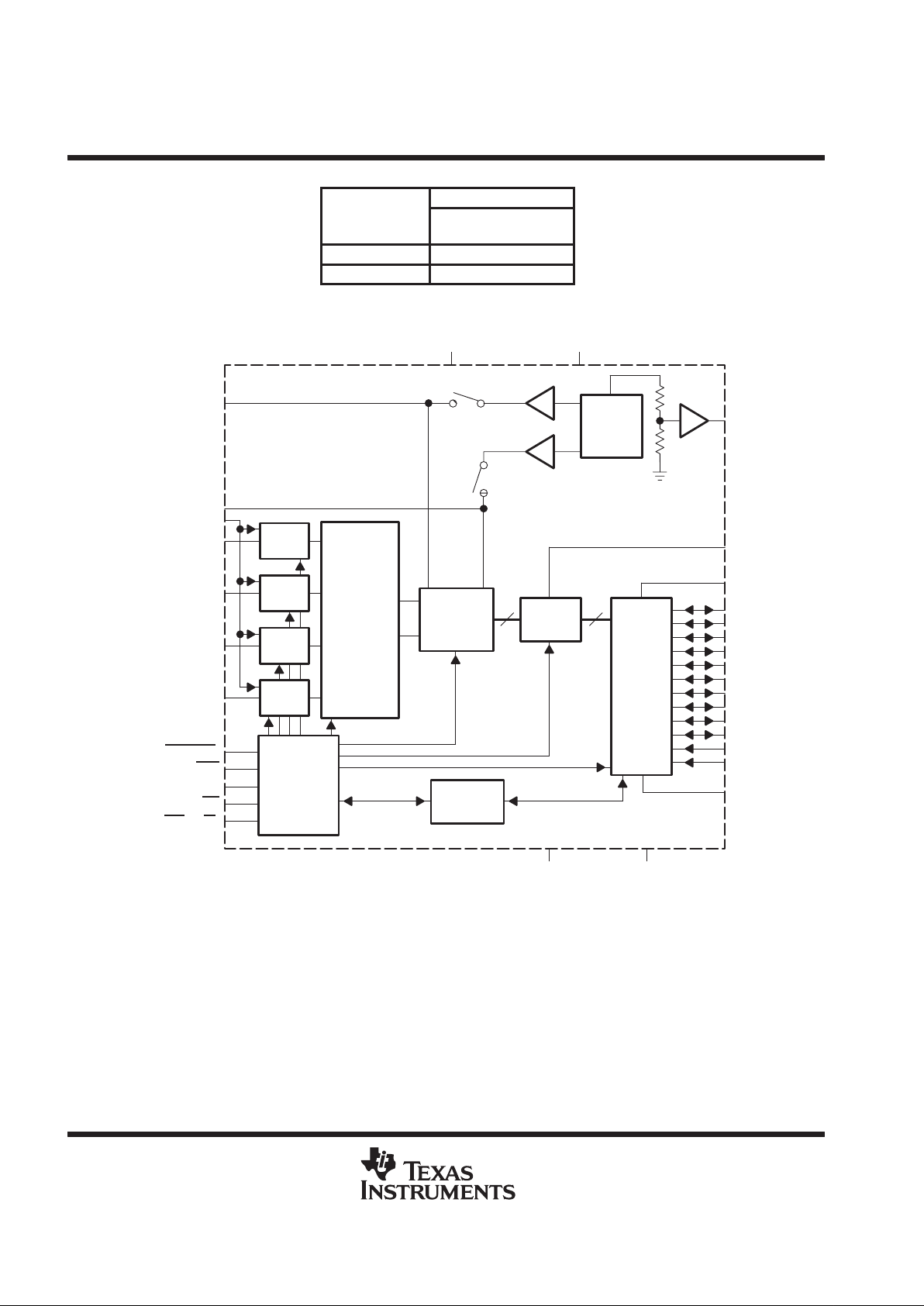
functional block diagram
Logic
and
Control
10 Bit
Pipeline
ADC
S/H
S/H
S/H
S/H
Single
Ended
and/or
Differential
MUX
+
–
V
REFP
V
REFM
1.5 V
3.5 V
1.225 V
REF
FIFO
16 × 10
10
10
Buffers
2.5 V
Control
Register
AV
DD
DV
DD
AGND DGND
REFOUT
DATA_AV
BV
DD
D0
D1
D2
D3
D4
D5
D6
D7
D8
D9
RA0
RA1
BGND
REFP
REFM
AINP
AINM
BINP
BINM
CONV_CLK (CONVST
)
CS0
CS1
RD
WR (R/W)
REFIN
Page 3
THS10064
10-BIT 6 MSPS, SIMULTANEOUS SAMPLING
ANALOG-TO-DIGITAL CONVERTER
SLAS255 – DECEMBER 1999
3
POST OFFICE BOX 655303 • DALLAS, TEXAS 75265
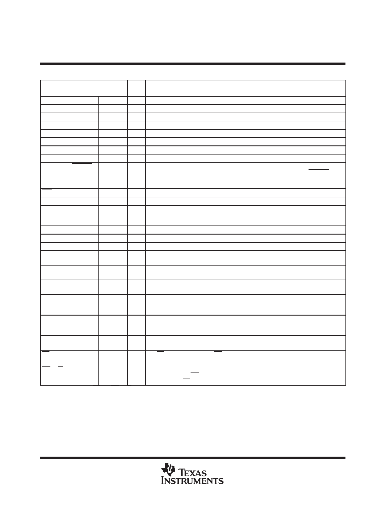
Terminal Functions
TERMINAL
NAME NO.
I/O
DESCRIPTION
AINP 32 I Analog input, single-ended or positive input of differential channel A
AINM 31 I Analog input, single-ended or negative input of differential channel A
BINP 30 I Analog input, single-ended or positive input of differential channel B
BINM 29 I Analog input, single-ended or negative input of differential channel B
AV
DD
23 I Analog supply voltage
AGND 24 I Analog ground
BV
DD
7 I Digital supply voltage for buffer
BGND 8 I Digital ground for buffer
CONV_CLK (CONVST) 15 I Digital input. This input is used to apply an external conversion clock in continuous conversion
mode. In single conversion mode, this input functions as the conversion start (CONVST
) input.
A high to low transition on this input holds simultaneously the selected analog input channels
and initiates a single conversion of all selected analog inputs.
CS0 22 I Chip select input (active low)
CS1 21 I Chip select input (active high)
DATA_AV 16 O Data available signal, which can be used to generate an interrupt for processors and as a level
information of the internal FIFO. This signal can be configured to be active low or high and can
be configured as a static level or pulse output. See Table 14.
DGND 17 I Digital ground. Ground reference for digital circuitry.
DV
DD
18 I Digital supply voltage
D0 – D9 1–6, 9–12 I/O/Z Digital input, output; D0 = LSB
RA0 13 I Digital input. RA0 is used as an address line for the control register . This is required for writing
to the control register 0 and control register 1. See Table 8.
RA1 14 I Digital input. RA1 is used as an address line for the control register . This is required for writing
to control register 0 and control register 1. See Table 8.
REFIN 28 I Common-mode reference input for the analog input channels. It is recommended that this pin
be connected to the reference output REFOUT.
REFP 26 I Reference input, requires a bypass capacitor of 10 µF to AGND in order to bypass the internal
reference voltage. An external reference voltage at this input can be applied. This option can
be programmed through control register 0. See Table 9.
REFM 25 I Reference input, requires a bypass capacitor of 10 µF to AGND in order to bypass the internal
reference voltage. An external reference voltage at this input can be applied. This option can
be programmed through control register 0. See Table 9.
REFOUT 27 O Analog fixed reference output voltage of 2.5 V. Sink and source capability of 250 µA. The
reference output requires a capacitor of 10 µF to AGND for filtering and stability .
RD
†
19 I The RD input is used only if the WR input is configured as a write only input. In this case, it is a
digital input, active low as a data read select from the processor. See timing section.
WR (R/W)
†
20 I This input is programmable. It functions as a read-write input R/W and can also be configured
as a write-only input WR
, which is active low and used as data write select from the processor.
In this case, the RD
input is used as a read input from the processor. See timing section.
†
The start-conditions of RD
and WR (R/W) are unknown. The first access to the ADC has to be a write access to initialize the ADC.
Page 4
THS10064
10-BIT 6 MSPS, SIMULTANEOUS SAMPLING
ANALOG-TO-DIGITAL CONVERTER
SLAS255 – DECEMBER 1999
4
POST OFFICE BOX 655303 • DALLAS, TEXAS 75265
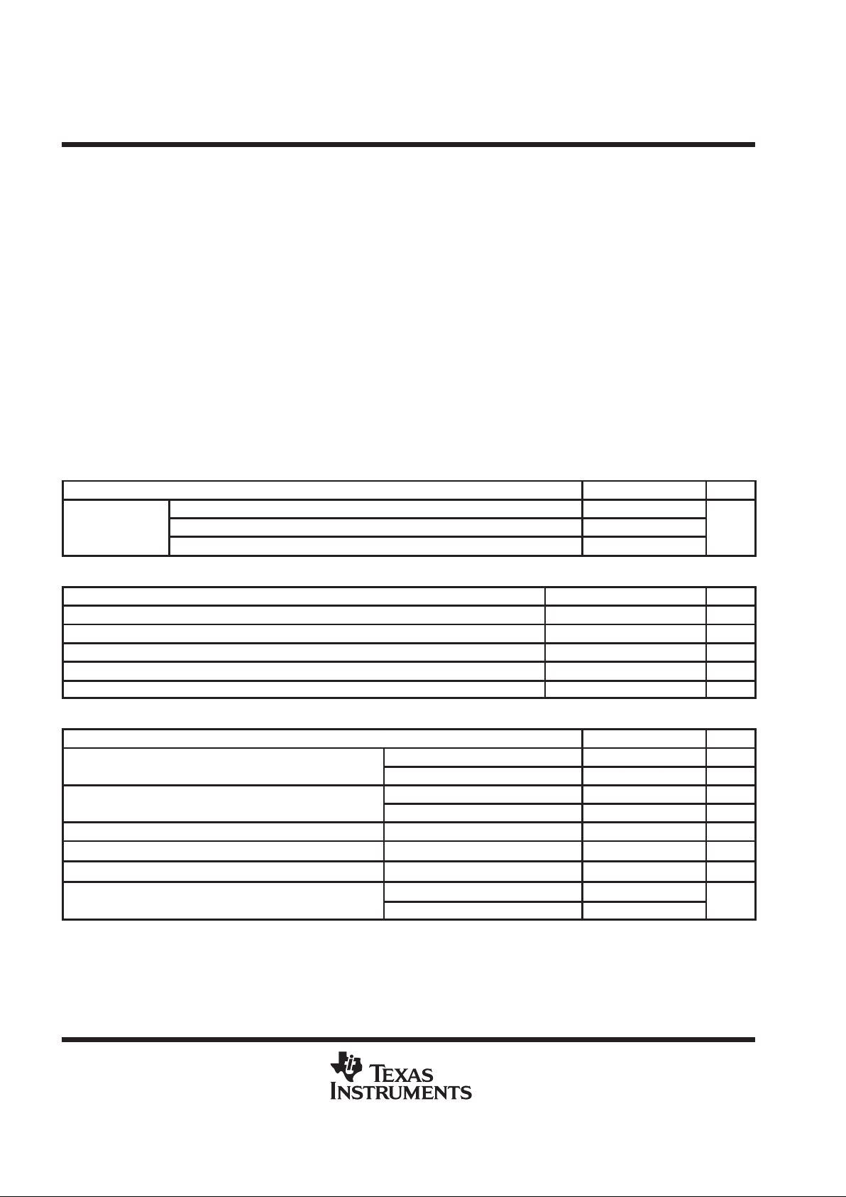
absolute maximum ratings over operating free-air temperature (unless otherwise noted)
†
Supply voltage range, DGND to DVDD –0.3 V to 6.5 V. . . . . . . . . . . . . . . . . . . . . . . . . . . . . . . . . . . . . . . . . . . . . .
BGND to BVDD –0.3 V to 6.5 V. . . . . . . . . . . . . . . . . . . . . . . . . . . . . . . . . . . . . . . . . . . . . .
AGND to AV
DD
–0.3 V to 6.5 V. . . . . . . . . . . . . . . . . . . . . . . . . . . . . . . . . . . . . . . . . . . . . . .
Analog input voltage range AGND – 0.3 V to AVDD + 1.5 V. . . . . . . . . . . . . . . . . . . . . . . . . . . . . . . . . . . . . . . . . .
Reference input voltage –0.3 + AGND to AVDD + 0.3 V. . . . . . . . . . . . . . . . . . . . . . . . . . . . . . . . . . . . . . . . . . . .
Digital input voltage range –0.3 V to BVDD/DVDD + 0.3 V. . . . . . . . . . . . . . . . . . . . . . . . . . . . . . . . . . . . . . . . . . .
Operating virtual junction temperature range, TJ –40°C to 150°C. . . . . . . . . . . . . . . . . . . . . . . . . . . . . . . . . . . . .
Operating free-air temperature range,T
A
THS10064C 0°C to 70°C. . . . . . . . . . . . . . . . . . . . . . . . . . . . . . . . . .
THS10064I –40°C to 85°C. . . . . . . . . . . . . . . . . . . . . . . . . . . . . . . . .
Storage temperature range, T
stg
–65°C to 150°C. . . . . . . . . . . . . . . . . . . . . . . . . . . . . . . . . . . . . . . . . . . . . . . . . . .
Lead temperature 1,6 mm (1/16 inch) from case for 10 seconds 260°C. . . . . . . . . . . . . . . . . . . . . . . . . . . . . . .
†
Stresses beyond those listed under “absolute maximum ratings” may cause permanent damage to the device. These are stress ratings only, and
functional operation of the device at these or any other conditions beyond those indicated under “recommended operating conditions” is not
implied. Exposure to absolute-maximum-rated conditions for extended periods may affect device reliability.
recommended operating conditions
power supply
MIN NOM MAX UNIT
AV
DD
4.75 5 5.25
Supply voltage
DV
DD
3 3.3 5.25
V
BV
DD
3 3.3 5.25
analog and reference inputs
MIN NOM MAX UNIT
Analog input voltage in single-ended configuration V
REFM
V
REFP
V
Common-mode input voltage VCM in differential configuration 1 2.5 4 V
External reference voltage,V
REFP
(optional) 3.5 AVDD–1.2 V
External reference voltage, V
REFM
(optional) 1.4 1.5 V
Input voltage difference, REFP – REFM 2 V
digital inputs
MIN NOM MAX UNIT
p
BVDD = 3.3 V 2 V
High-level input voltage, V
IH
BVDD = 5.25 V 2.6 V
p
BVDD = 3.3 V 0.6 V
Low-level input voltage, V
IL
BVDD = 5.25 V 0.6 V
Input CONV_CLK frequency DVDD = 3 V to 5.25 V 0.1 6 MHz
CONV_CLK pulse duration, clock high, t
w(CONV_CLKH)
DVDD = 3 V to 5.25 V 80 83 5000 ns
CONV_CLK pulse duration, clock low, t
w(CONV_CLKL)
DVDD = 3 V to 5.25 V 80 83 5000 ns
p
p
THS10064CDA 0 70
°
Operating free-air temperature, T
A
THS10064IDA –40 85
°C
Page 5
THS10064
10-BIT 6 MSPS, SIMULTANEOUS SAMPLING
ANALOG-TO-DIGITAL CONVERTER
SLAS255 – DECEMBER 1999
5
POST OFFICE BOX 655303 • DALLAS, TEXAS 75265
electrical characteristics over recommended operating conditions, DVDD = 3.3 V , A VDD = 5 V , V
REF
= internal (unless otherwise noted)
digital specifications
PARAMETER TEST CONDITIONS MIN TYP MAX UNIT
Digital inputs
I
IH
High-level input current DVDD = digital inputs –50 50 µA
I
IL
Low-level input current Digital input = 0 V –50 50 µA
C
i
Input capacitance 5 pF
Digital outputs
V
OH
High-level output voltage I
OH
= –50 µA, BVDD = 3.3 V, 5 V BVDD–0.5 V
V
OL
Low-level output voltage I
OL
= 50 µA, BVDD = 3.3 V, 5 V 0.4 V
I
OZ
High-impedance-state output current CS1 = DGND, CS0 = DV
DD
–10 10 µA
C
O
Output capacitance 5 pF
C
L
Load capacitance at databus D0 – D11 30 pF
Page 6
THS10064
10-BIT 6 MSPS, SIMULTANEOUS SAMPLING
ANALOG-TO-DIGITAL CONVERTER
SLAS255 – DECEMBER 1999
6
POST OFFICE BOX 655303 • DALLAS, TEXAS 75265
electrical characteristics over recommended operating conditions, AVDD = 5 V,
DV
DD
= BVDD = 3.3 V, fs = 6 MSPS, V
REF
= internal (unless otherwise noted) (continued)
dc specifications
PARAMETER TEST CONDITIONS MIN TYP MAX UNIT
Resolution 10 Bits
Accuracy
Integral nonlinearity, INL ±1 LSB
Differential nonlinearity , DNL ±1 LSB
After calibration in single-ended mode –15 15 mV
Offset error
After calibration in differential mode –5 5 mV
Gain error 1% FSR
Analog input
Input capacitance 15 pF
Input leakage current V
AIN
= V
REFM
to V
REFP
±10 µA
Internal voltage reference
Accuracy, V
REFP
3.33 3.5 3.67 V
Accuracy, V
REFM
1.42 1.5 1.58 V
T emperature coef ficient 50 PPM/°C
Reference noise 100 µV
Accuracy, REFOUT 2.475 2.5 2.525 V
Power supply
I
DDA
Analog supply current AVDD =5 V, BVDD = DVDD = 3.3 V 36 40 mA
I
DDD
Digital supply voltage AVDD = 5 V, BVDD = DVDD = 3.3 V 0.5 1 mA
I
DDB
Buffer supply voltage AVDD = 5 V, BVDD = DVDD = 3.3 V 1.5 4 mA
I
DD_P
Supply current in power-down mode AVDD = 5 V, BVDD = DVDD = 3.3 V 7 mA
Power dissipation AVDD = 5 V, DVDD = BVDD = 3.3 V 186 216 mW
Power dissipation in power down AVDD = 5 V, DVDD = BVDD = 3.3 V 30 mW
Page 7
THS10064
10-BIT 6 MSPS, SIMULTANEOUS SAMPLING
ANALOG-TO-DIGITAL CONVERTER
SLAS255 – DECEMBER 1999
7
POST OFFICE BOX 655303 • DALLAS, TEXAS 75265
electrical characteristics over recommended operating conditions, V
REF
= internal, fs = 6 MHz,
f
I
= 2 MHz at –1dBFS (unless otherwise noted) (continued)
ac specifications, AVDD = 5 V, BVDD = DVDD = 3.3 V, CL < 30 pF
PARAMETER TEST CONDITIONS MIN TYP MAX UNIT
Differential mode 56 59 dB
SINAD Signal-to-noise ratio + distortion
Single-ended mode
(see Note 1)
59 dB
Differential mode 59 61 dB
SNR Signal-to-noise ratio
Single-ended mode
(see Note 1)
60 dB
Differential mode –67 –61 dB
THD
T otal harmonic distortion
Single-ended mode –67 dB
Differential mode 9 9.6 Bits
ENOB
(SNR)
Effective number of bits
Single-ended mode
(see Note 1)
9.5 Bits
p
Differential mode 61 68 dB
SFDR
Spurious free dynamic range
Single-ended mode 68 dB
Analog Input
Full-power bandwidth with a source impedance of 150 Ω in
differential configuration.
Full scale sinewave, –3 dB 96 MHz
Full-power bandwidth with a source impedance of 150 Ω in
single-ended configuration.
Full scale sinewave, –3 dB 54 MHz
Small-signal bandwidth with a source impedance of 150 Ω in
differential configuration.
100 mVpp sinewave, –3 dB 96 MHz
Small-signal bandwidth with a source impedance of 150 Ω in
single-ended configuration.
100 mVpp sinewave, –3 dB 54 MHz
NOTE 1: The SNR (ENOB) and SINAD is degraded typically by 2 dB in single-ended mode when the reading of data is asynchronous to the
sampling clock.
Page 8
THS10064
10-BIT 6 MSPS, SIMULTANEOUS SAMPLING
ANALOG-TO-DIGITAL CONVERTER
SLAS255 – DECEMBER 1999
8
POST OFFICE BOX 655303 • DALLAS, TEXAS 75265
timing specifications, AV
DD
= 5 V, BVDD = DVDD = 3.3 V, V
REF
= internal, CL < 30 pF
PARAMETER TEST CONDITIONS MIN TYP MAX UNIT
t
d(DATA_AV)
Delay time 5 ns
t
d(o)
Delay time 5 ns
t
pipe
Latency 5
CONV
CLK
timing specification of the single conversion mode
†
PARAMETER TEST CONDITIONS MIN TYP MAX UNIT
t
c
Clock cycle of the internal clock oscillator 159 167 175 ns
t
w1
Pulse width, CONVST 1.5×t
c
ns
t
dA
Aperture time 1 ns
1 analog input 2×t
c
2 analog inputs 3×t
c
ns
t2Time between consecutive start of single conversion
3 analog inputs 4×t
c
4 analog inputs 5×t
c
ns
1 analog input, TL = 1 6×t
c
Delay time, DATA_AV becomes active for the trigger
2 analog inputs, TL = 2 7×t
c
ns
y, _ gg
level condition: TRIG0 = 0, TRIG1 = 0
3 analog inputs, TL = 3 8×t
c
4 analog inputs, TL = 4 9×t
c
ns
1 analog input, TL = 4 3×t2 +6×t
c
Delay time, DATA_AV becomes active for the trigger
2 analog inputs, TL = 4 t2 +7×t
c
ns
t
d(DATA_AV)
y, _ gg
level condition: TRIG0 = 1, TRIG1 = 0
3 analog inputs, TL = 6 t2 +8×t
c
4 analog inputs, TL = 8 t2 +9×t
c
ns
1 analog input, TL = 8 7×t2 +6×t
c
Delay time, DATA_AV becomes active for the trigger
2 analog inputs, TL = 8 3×t2 +7×t
c
ns
y, _ gg
level condition: TRIG0 = 0, TRIG1 = 1
3 analog inputs, TL = 9 2×t2 +8×t
c
4 analog inputs, TL = 12 2×t2 +9×t
c
ns
1 analog input, TL = 14 13×t2 +6×t
c
t
d(DATA_AV)
Delay time, DATA_AV becomes active for the trigger
2 analog inputs, TL = 12 5×t2 +7×t
c
ns
(
_
)
level condition: TRIG0 = 1, TRIG1 = 1
3 analog inputs, TL = 12 3×t2 +8×t
c
ns
†
Timing parameters are ensured by design but are not tested.
Page 9
THS10064
10-BIT 6 MSPS, SIMULTANEOUS SAMPLING
ANALOG-TO-DIGITAL CONVERTER
SLAS255 – DECEMBER 1999
9
POST OFFICE BOX 655303 • DALLAS, TEXAS 75265
detailed description
reference voltage
The THS10064 has a built-in reference, which provides the reference voltages for the ADC. VREFP is set to
3.5 V and VREFM is set to 1.5 V . An external reference can also be used through two reference input pins, REFP
and REFM, if the reference source is programmed as external. The voltage levels applied to these pins establish
the upper and lower limits of the analog inputs to produce a full-scale and zero-scale reading respectively.
analog inputs
The THS10064 consists of 4 analog inputs, which are sampled simultaneously . These inputs can be selected
individually and configured as single-ended or differential inputs. The desired analog input channel can be
programmed.
analog-to-digital converter
The THS10064 uses a 10-bit pipelined multistaged architecture with 4 1-bit stages followed by 4 2-bit stages,
which achieves a high sample rate with low power consumption. The THS10064 distributes the conversion over
several smaller ADC sub-blocks, refining the conversion with progressively higher accuracy as the device
passes the results from stage to stage. This distributed conversion requires a small fraction of the number of
comparators used in a traditional flash ADC. A sample-and-hold amplifier (SHA) within each of the stages
permits the first stage to operate on a new input sample while the second through the eighth stages operate
on the seven preceding samples.
conversion modes
The conversion can be performed in two different conversion modes. In the single conversion mode, the
conversion is initiated by an external signal (CONVST). An internal oscillator controls the conversion time. In
the continuous conversion mode, an external clock signal is applied to the clock input (CONV_CLK). A new
conversion is started with every falling edge of the applied clock signal.
sampling rate
The maximum possible conversion rate per channel is dependent on the selected analog input channels. T able
1 shows the maximum conversion rate in the continuous conversion mode for different combinations.
Table 1. Maximum Conversion Rate in Continuous Conversion Mode
CHANNEL CONFIGURATION
NUMBER OF
CHANNELS
MAXIMUM CONVERSION
RATE PER CHANNEL
1 single-ended channel 1 6 MSPS
2 single-ended channels 2 3 MSPS
3 single-ended channels 3 2 MSPS
4 single-ended channels 4 1.5 MSPS
1 differential channel 1 6 MSPS
2 differential channels 2 3 MSPS
1 single-ended and 1 differential channel 2 3 MSPS
2 single-ended and 1 differential channels 3 2 MSPS
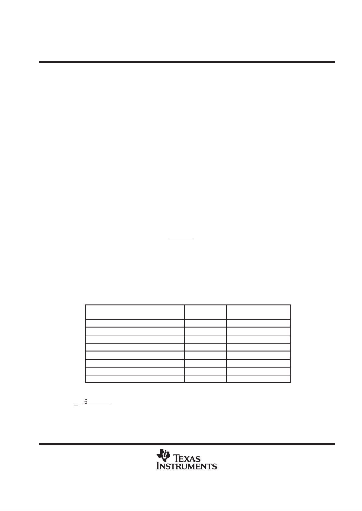
The maximum conversion rate in the continuous conversion mode per channel, fc, is given by:
fc
+
6 MSPS
# channels
Table 2 shows the maximum conversion rate in the single conversion mode.
Page 10
THS10064
10-BIT 6 MSPS, SIMULTANEOUS SAMPLING
ANALOG-TO-DIGITAL CONVERTER
SLAS255 – DECEMBER 1999
10
POST OFFICE BOX 655303 • DALLAS, TEXAS 75265
sampling rate (continued)
Table 2. Maximum Conversion Rate in Single Conversion Mode
CHANNEL CONFIGURATION
NUMBER OF
CHANNELS
MAXIMUM CONVERSION
RATE PER CHANNEL
1 single-ended channel 1 3 MSPS
2 single-ended channels 2 2 MSPS
3 single-ended channels 3 1.5 MSPS
4 single-ended channels 4 1.2 MSPS
1 differential channel 1 3 MSPS
2 differential channels 2 2 MSPS
1 single-ended and 1 differential channel 2 1.5 MSPS
2 single-ended and 1 differential channels 3 1.2 MSPS
single conversion mode
In single conversion mode, a single conversion of the selected analog input channels is performed. The single
conversion mode is selected by setting bit 1 of control register 0 to 1.
A single conversion is initiated by pulsing the CONVST input. On the falling edge of CONVST, the sample and
hold stages of the selected analog inputs are placed into hold simultaneously, and the conversion sequence
for the selected channels is started.
The conversion clock in single conversion mode is generated internally using a clock oscillator circuit. The signal
DATA_AV (data available) becomes active when the trigger level is reached and indicates that the converted
sample(s) is (are) written into the FIFO and can be read out. The trigger level in the single conversion mode
can be selected according to Table 13.
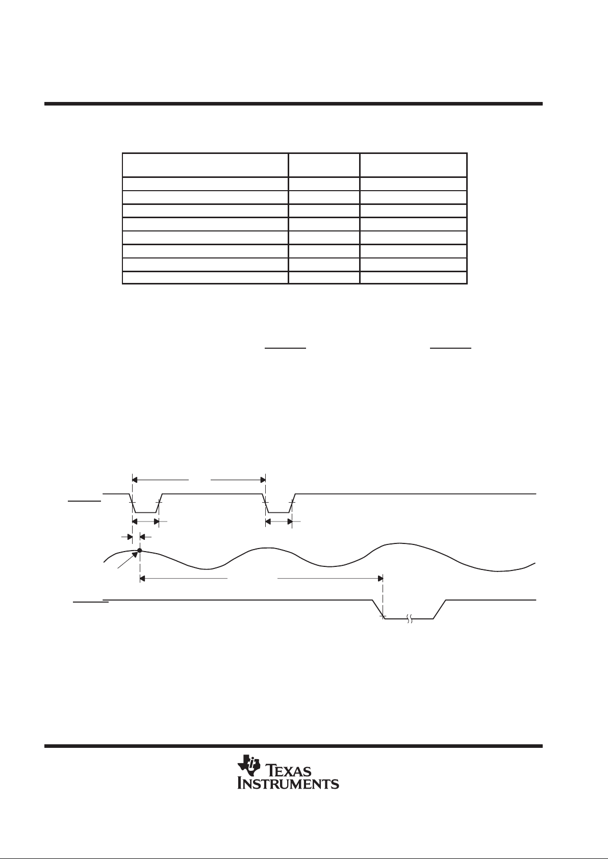
Figure 1 shows the timing of the single conversion mode. In this mode, up to four analog input channels can
be selected to be sampled simultaneously (see Table 2).
CONVST
AIN
Sample N
t
1
t
1
t
d(A)
t
2
t
DATA_AV
DATA_AV,
Trigger Level = 1
Figure 1. Timing of Single Conversion Mode
The time (t2) between consecutive starts of single conversions is dependent on the number of selected analog
input channels. The time t
DATA_AV
, until DA TA_AV becomes active is given by: t
DATA_AV
= t
pipe
+ n × tc. This
equation is valid for a trigger level which is equivalent to the number of selected analog input channels. For all
other trigger level conditions refer to the timing specifications of single conversion mode.
Page 11
THS10064
10-BIT 6 MSPS, SIMULTANEOUS SAMPLING
ANALOG-TO-DIGITAL CONVERTER
SLAS255 – DECEMBER 1999
11
POST OFFICE BOX 655303 • DALLAS, TEXAS 75265
continuous conversion mode
The internal clock oscillator used in the single-conversion mode is switched off in continuous conversion mode.
In continuous conversion mode, (bit 1 of control register 0 set to 0) the ADC operates with a free running
external clock signal CONV_CLK. With every rising edge of the CONV_CLK signal a new converted value is
written into the FIFO. The first conversion value is written into the FIFO with a latency of 8 + TL (trigger level)
clock cycles after the FIFO reset.
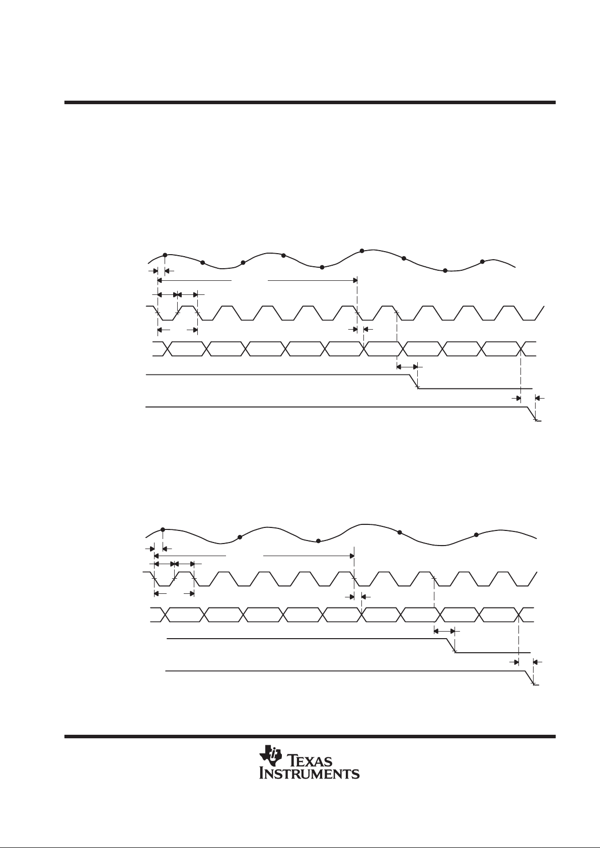
Figure 2 shows the timing of continuous conversion mode when one analog input channel is selected. The
maximum throughput rate is 6 MSPS in this mode. The timing of the DA T A_A V signal is shown here in the case
of a trigger level set to 1 or 4.
Sample N
Channel 1
Sample N+1
Channel 1
Sample N+2
Channel 1
Sample N+3
Channel 1
Sample N+4
Channel 1
Sample N+5
Channel 1
Sample N+6
Channel 1
Sample N+7
Channel 1
Sample N+8
Channel 1
Data N–5
Channel 1
Data N–4
Channel 1
Data N–3
Channel 1
Data N–2
Channel 1
Data N–1
Channel 1
Data N
Channel 1
Data N+1
Channel 1
Data N+2
Channel 1
Data N+3
Channel 1
t
d(A)
t
w(CONV_CLKH)
t
w(CONV_CLKL)
t
c
t
d(O)
t
d(DATA_AV)
t
d(DATA_AV)
AIN
CONV_CLK
Data Into
FIFO
DATA_AV,
Trigger Level = 1
DATA_AV,
Trigger Level = 4
t
d(pipe)
50% 50%
Figure 2. Timing of Continuous Conversion Mode (1-channel operation)
Figure 3 shows the timing of continuous conversion mode when two analog input channels are selected. The
maximum throughput rate per channel is 3 MSPS in this mode. The data flow in the bottom of the figure shows
the order the converted data is written into the FIFO. The timing of the DA TA_A V signal shown here is for a trigger
level set to 2 or 4.
AIN
CONV_CLK
Data Into
FIFO
DATA_AV,
Trigger Level = 2
DATA_AV,
Trigger Level = 4
Data N–3
Channel 2
Data N–2
Channel 1
Data N–2
Channel 2
Data N–1
Channel 1
Data N–1
Channel 2
Data N
Channel 1
Data N
Channel 2
Data N+1
Channel 1
Data N+1
Channel 2
t
d(DATA_AV)
t
w(CONV_CLKH)
t
w(CONV_CLKL)
t
d(A)
Sample N
Channel 1,2
Sample N+1
Channel 1,2
Sample N+2
Channel 1,2
Sample N+3
Channel 1,2
Sample N+4
Channel 1,2
t
c
t
d(O)
t
d(Pipe)
t
d(DATA_AV)
50% 50%
Figure 3. Timing of Continuous Conversion Mode (2-channel operation)
Page 12
THS10064
10-BIT 6 MSPS, SIMULTANEOUS SAMPLING
ANALOG-TO-DIGITAL CONVERTER
SLAS255 – DECEMBER 1999
12
POST OFFICE BOX 655303 • DALLAS, TEXAS 75265
continuous conversion mode (continued)
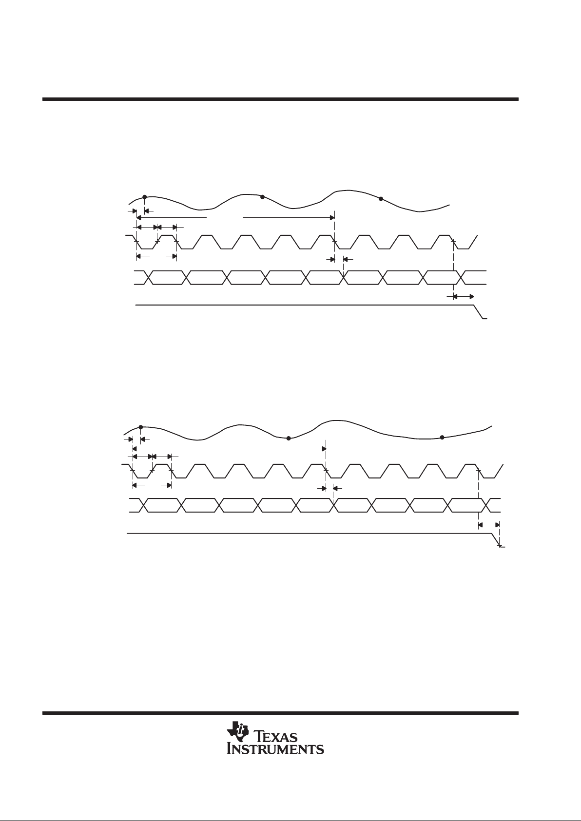
Figure 4 shows the timing of continuous conversion mode when three analog input channels are selected. The
maximum throughput rate per channel is 2 MSPS in this mode. The data flow in the bottom of the figure shows
in which order the converted data is written into the FIFO. The timing of the DA TA_AV signal shown here is for
a trigger level set to 3.
AIN
CONV_CLK
Data Into
FIFO
DATA_AV,
Trigger Level = 3
t
d(DATA_AV)
Sample N
Channel 1,2,3
Sample N+1
Channel 1,2,3
Sample N+2
Channel 1,2,3
t
d(O)
Data N–2
Channel 2
Data N–2
Channel 3
Data N–1
Channel 1
Data N–1
Channel 2
Data N–1
Channel 3
Data N
Channel 1
Data N
Channel 2
Data N
Channel 3
t
c
t
d(A)
t
w(CONV_CLKH)
t
w(CONV_CLKL)
t
d(Pipe)
50% 50%
Figure 4. Timing of Continuous Conversion Mode (3-channel operation)
Figure 5 shows the timing of continuous conversion mode when four analog input channels are selected. The
maximum throughput rate per channel is 1.5 MSPS in this mode. The data flow in the bottom of the figure shows
in which order the converted data is written into the FIFO. The timing of the DA TA_AV signal shown here is for
a trigger level of 4.
AIN
CONV_CLK
Data Into
FIFO
DATA_AV,
Trigger Level = 4
t
w(CONV_CLKH)
Sample N
Channel 1,2,3,4
Sample N+1
Channel 1,2,3,4
Sample N+2
Channel 1,2,3,4
t
d(Pipe)
t
w(CONV_CLKL)
t
c
t
d(O)
Data N–2
Channel 4
Data N–1
Channel 1
Data N–1
Channel 2
Data N–1
Channel 3
Data N–1
Channel 4
Data N
Channel 1
Data N
Channel 2
Data N
Channel 3
Data N
Channel 4
t
d(DATA_AV)
t
d(A)
50% 50%
Figure 5. Timing of Continuous Conversion Mode (4-channel operation)
Page 13
THS10064
10-BIT 6 MSPS, SIMULTANEOUS SAMPLING
ANALOG-TO-DIGITAL CONVERTER
SLAS255 – DECEMBER 1999
13
POST OFFICE BOX 655303 • DALLAS, TEXAS 75265
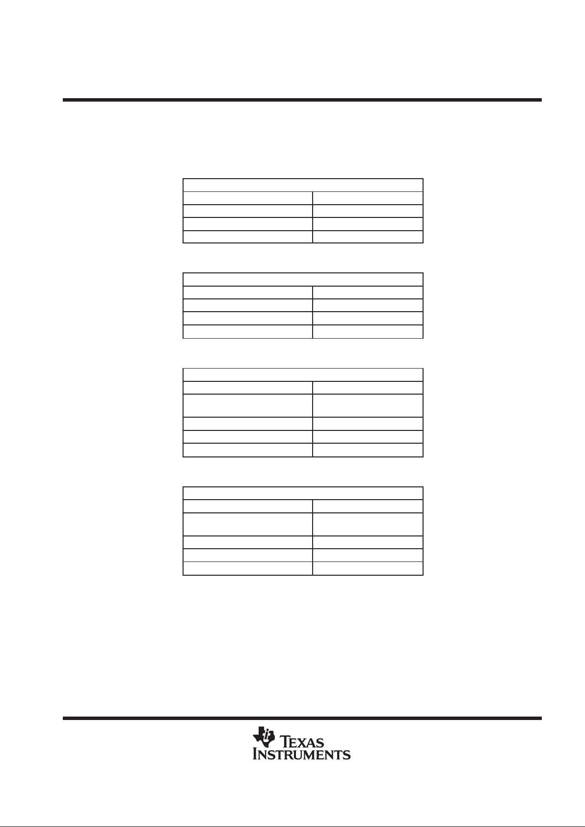
digital output data format
The digital output data format of the THS10064 can either be in binary format or in two’s complement format.
The following tables list the digital outputs for the analog input voltages.
Table 3. Binary Output Format for Single-Ended Configuration
SINGLE-ENDED, BINARY OUTPUT
ANALOG INPUT VOLTAGE DIGITAL OUTPUT CODE
AIN = V
REFP
3FFh
AIN = (V
REFP
+ V
REFM
)/2 200h
AIN = V
REFM
000h
Table 4. Two’s Complement Output Format for Single-Ended Configuration
SINGLE-ENDED, TWOS COMPLEMENT
ANALOG INPUT VOLTAGE DIGITAL OUTPUT CODE
AIN = V
REFP
1FFh
AIN = (V
REFP
+ V
REFM
)/2 000h
AIN = V
REFM
200h
Table 5. Binary Output Format for Differential Configuration
DIFFERENTIAL, BINARY OUTPUT
ANALOG INPUT VOLTAGE DIGITAL OUTPUT CODE
Vin = AINP – AINM
V
REF
= V
REFP
– V
REFM
Vin = V
REF
3FFh
Vin = 0 200h
Vin = –V
REF
000h
Table 6. Two’s Complement Output Format for Differential Configuration
DIFFERENTIAL, BINARY OUTPUT
ANALOG INPUT VOLTAGE DIGITAL OUTPUT CODE
Vin = AINP – AINM
V
REF
= V
REFP
– V
REFM
Vin = V
REF
1FFh
Vin = 0 000h
Vin = –V
REF
200h
Page 14
THS10064
10-BIT 6 MSPS, SIMULTANEOUS SAMPLING
ANALOG-TO-DIGITAL CONVERTER
SLAS255 – DECEMBER 1999
14
POST OFFICE BOX 655303 • DALLAS, TEXAS 75265
FIFO description
In order to facilitate an efficient connection to today’s processors, the THS10064 is supplied with a FIFO. This
integrated FIFO enables a problem-free processing of data with today’s processors. The FIFO is provided as
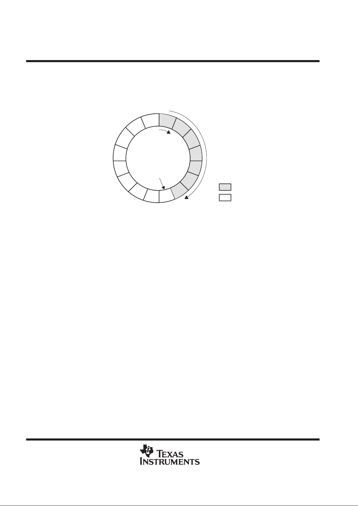
a flexible circular buffer . The circular buffer integrated in the THS10064 can store up to 16 conversion values.
Therefore, the amount of interrupts to be served by a processor can be reduced significantly.
8
9
10
11
12
13
14
15
16
1
2
3
4
5
6
7
Read Pointer
Trigger Pointer
Write Pointer
Data in FIFO
Free
Figure 6. Circular Buffer
The converted data of the THS10064 is automatically written into the FIFO. To control the writing and reading
process, a write pointer, a read pointer and a trigger pointer are used. The read pointer always shows the
location which will be read next. The write pointer indicates the location which contains the last written sample.
With a selection of multiple analog input channels, the converted values are written in a predefined sequence
to the circular buffer (autoscan mode). In this way, the channel information for the reading processor is
continually maintained.
The FIFO can be programmed through the control register of the ADC. The user has the ability to select a
specific trigger level according to Table 13 in order to choose the configuration which best fits the application.
The FIFO provides the signal DATA_AV, which signals the processor to read the amount of data equal to the
trigger level selected in Table 13. The signal DAT A_AV becomes active when the trigger condition is satisfied.
The trigger condition is satisfied when as many values as selected for the trigger level where written into the
FIFO.
The signal DA T A_AV could be connected to an interrupt input of a processor. In every interrupt service routine
call, the processor must read the amount of data equal to the trigger level from the ADC. The first data represents
the first channel according to the autoscan mode, which is shown in Table 10. The channel information is
therefore always maintained.
Page 15
THS10064
10-BIT 6 MSPS, SIMULTANEOUS SAMPLING
ANALOG-TO-DIGITAL CONVERTER
SLAS255 – DECEMBER 1999
15
POST OFFICE BOX 655303 • DALLAS, TEXAS 75265
Reading data from the FIFO
The THS10064 informs the connected processor via the digital output DA TA_AV (data available) that a block
of conversion values are ready to be read. The block size to be read is always equal to the setting of the trigger
level. The selectable trigger levels depend on the number of selected analog input channels. For example, when
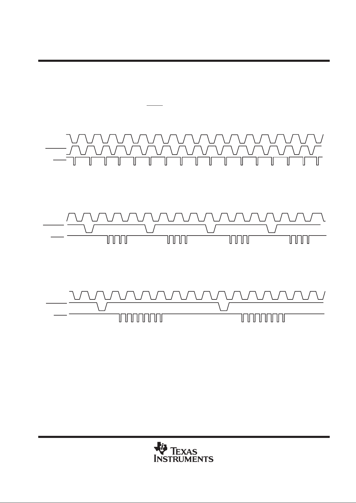
choosing one analog input, a trigger level of 1, 4, 8, and 14 can be selected. The following figures demonstrate
the principle of reading the data (the READ
signal is asynchronous to CONV_CLK).
In Figure 7, a trigger level of 1 is selected. The control signal DA TA_A V is set to an active low pulse. This means
that the connected processor has the task to read 1 value from the ADC after every DATA_AV low pulse.
CONV_CLK
DATA_AV
READ
Figure 7. Trigger Level 1 Selected
In Figure 8, a trigger level of 4 is selected. The control signal DA TA_A V is set to an active low pulse. This means
that the connected processor has the task to read 4 values from the ADC after every DATA_AV low pulse.
CONV_CLK
DATA_AV
READ
Figure 8. Trigger Level 4 Selected
In Figure 9, a trigger level of 8 is selected. The control signal DA TA_A V is set to an active low pulse. This means
that the connected processor has the task to read 8 values from the ADC after every DATA_AV low pulse.
CONV_CLK
DATA_AV
READ
Figure 9. Trigger Level 8 Selected
Page 16
THS10064
10-BIT 6 MSPS, SIMULTANEOUS SAMPLING
ANALOG-TO-DIGITAL CONVERTER
SLAS255 – DECEMBER 1999
16
POST OFFICE BOX 655303 • DALLAS, TEXAS 75265
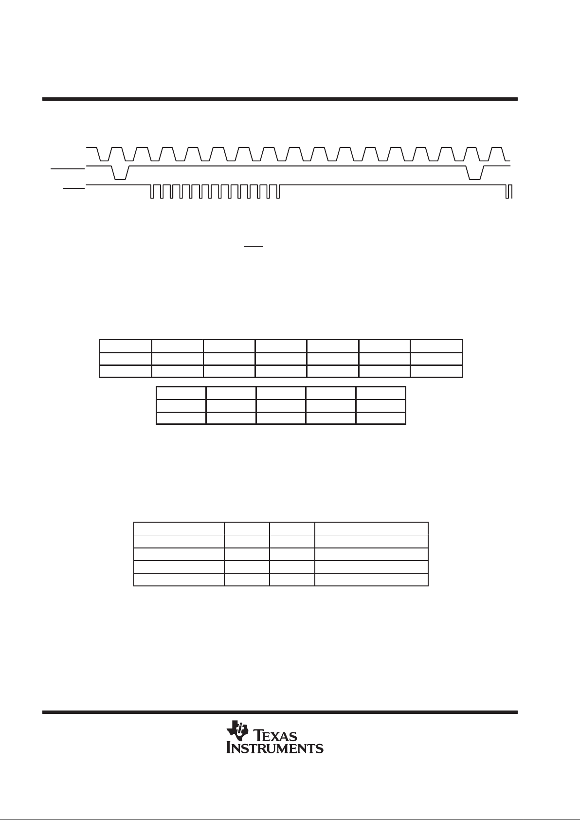
In Figure 10, a trigger level of 14 is selected. The control signal DATA_AV is set to an active low pulse. This
means that the connected processor has the task to read 14 values from the ADC after every DATA_AV low
pulse.
CONV_CLK
DATA_AV
READ
Figure 10. Trigger Level 14 Selected
READ is always the logical combination of CS0
, CS1 and RD.
ADC Control Register
The THS10064 contains two 10-bit wide control registers (CR0, CR1) in order to program the device into the
desired mode. The bit definitions of both control registers are shown in Table 7.
Table 7. Bit Definitions of Control Register CR0 and CR1
BIT BIT 5 BIT 4 BIT 3 BIT 2 BIT 1 BIT 0
CR0 DIFF0 CHSEL1 CHSEL0 PD MODE VREF
CR1 DATA_P DATA_T TRIG1 TRIG0 OVFL/FRST RESET
BIT BIT 9 BIT 8 BIT 7 BIT 6
CR0 TEST1 TEST0 SCAN DIFF1
CR1 RESERVED OFFSET BIN/2’s R/W
Writing to control register 0 and control register 1
The 10-bit wide control register 0 and control register 1 can be programmed by addressing the desired control
register and writing the register value to the ADC. The addressing is performed with the upper bits RA0 and RA1.
During this write process, the data bits D0 to D9 contain the desired control register value. Table 8 shows the
addressing of each control register.
Table 8. Control Register Addressing
D0 – D9 RA0 RA1 Addressed Control Register
Desired register value 0 0 Control register 0
Desired register value 1 0 Control register 1
Desired register value 0 1 Reserved for future
Desired register value 1 1 Reserved for future
Page 17
THS10064
10-BIT 6 MSPS, SIMULTANEOUS SAMPLING
ANALOG-TO-DIGITAL CONVERTER
SLAS255 – DECEMBER 1999
17
POST OFFICE BOX 655303 • DALLAS, TEXAS 75265
initialization of the THS10064
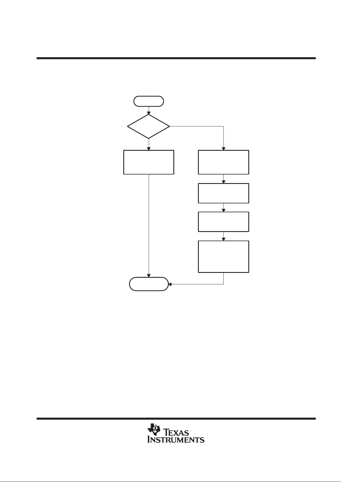
The initialization of the THS10064 should be done according to the configuration flow shown in Figure 11.
Start
Use Default
Values?
Yes
Write 0x401 to
THS10064
(Set Reset Bit in CR1)
No
Write 0x401 to
THS10064
(Set Reset Bit in
CR1)
Clear RESET By
Writing 0x400 to
CR1
Write The User
Configuration to
CR0
Write The User
Configuration to
CR1 (Can Include
FIFO Reset, Must
Exclude RESET)
Continue
Figure 11. THS10064 Configuration Flow
Page 18
THS10064
10-BIT 6 MSPS, SIMULTANEOUS SAMPLING
ANALOG-TO-DIGITAL CONVERTER
SLAS255 – DECEMBER 1999
18
POST OFFICE BOX 655303 • DALLAS, TEXAS 75265
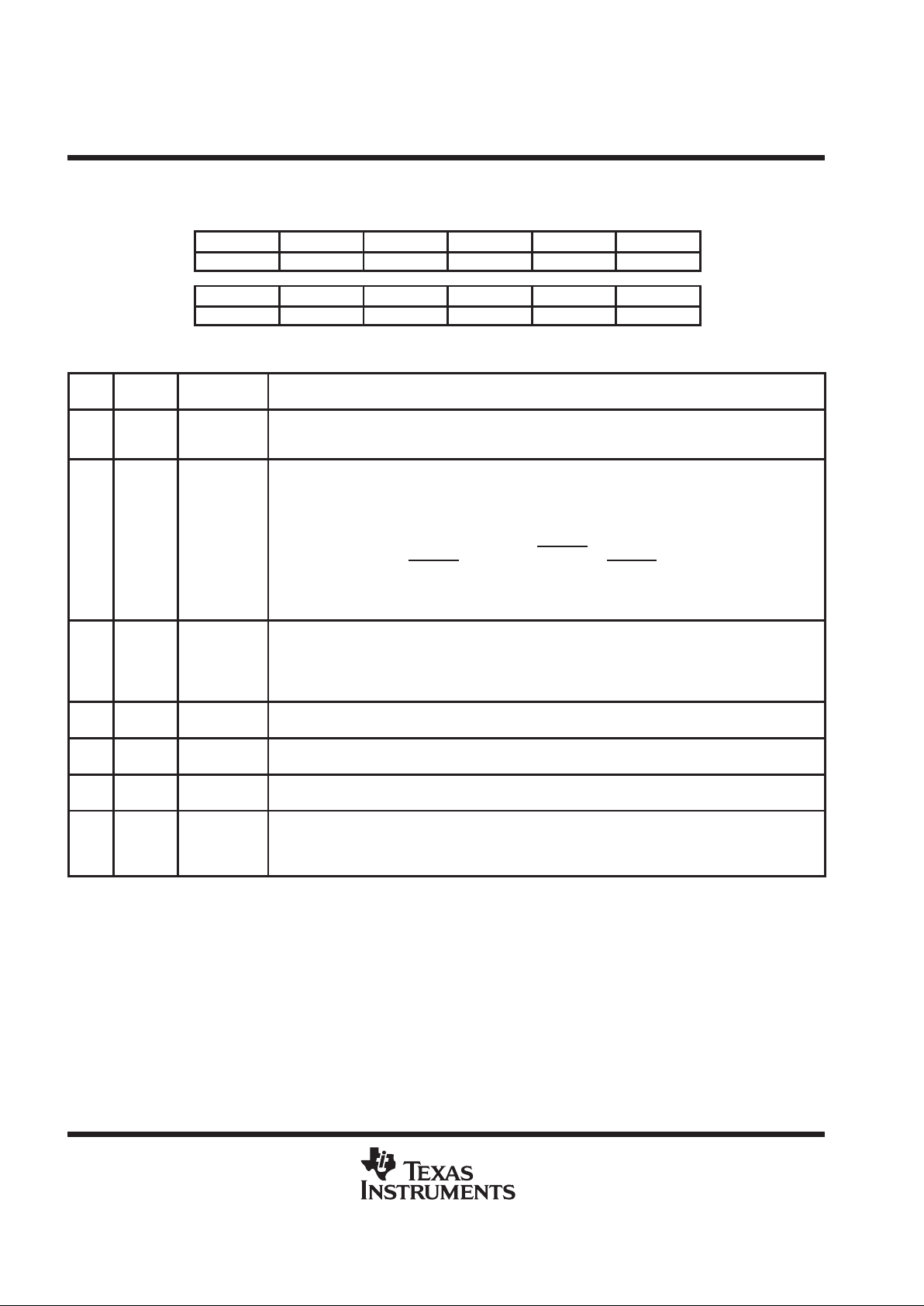
ADC control registers
control register 0 (see Table 8)
– – BIT 9 BIT 8 BIT 7 BIT 6
– – TEST1 TEST0 SCAN DIFF1
BIT 5 BIT 4 BIT 3 BIT 2 BIT 1 BIT 0
DIFF0 CHSEL1 CHSEL0 PD MODE VREF
Table 9. Control Register 0 Bit Functions
BITS
RESET
VALUE
NAME FUNCTION
0 0 VREF Vref select:
Bit 0 = 0 → The internal reference is selected
Bit 0 = 1 → The external reference voltage is selected
1 0 MODE Continuous conversion mode/single conversion mode
Bit 1 = 0 → Continuous conversion mode is selected
An external clock signal is applied to the CONV_CLK input in this mode. With every falling edge of the
CONV_CLK signal a new converted value is written into the FIFO.
Bit 1 = 1 → Single conversion mode is selected
In this mode, the CONV_CLK input functions as a CONVST
input. A single conversion is initiated on the
THS10064 by pulsing the CONVST
input. On the falling edge of CONVST , the sample and hold stages of
the selected analog inputs are placed into hold simultaneously, and the conversion sequence for the
selected channels is started. The signal DATA_AV (data available) becomes active when the trigger
condition is satisfied.
2 0 PD Power down.
Bit 2 = 0 → The ADC is active
Bit 2 = 1 → Power down
The reading and writing to and from the digital outputs is possible during power down. It is also possible to
read out the FIFO.
3, 4 0,0 CHSEL0,
CHSEL1
Channel select
Bit 3 and bit 4 select the analog input channel of the ADC. Refer to Table 10.
5,6 1,0 DIFF0, DIFF1 Number of differential channels
Bit 5 and bit 6 contain information about the number of selected differential channels. Refer to T able 10.
7 0 SCAN Autoscan enable
Bit 7 enables or disables the autoscan function of the ADC. Refer to Table 10.
8,9 0,0 TEST0,
TEST1
Test input enable
Bit 8 and bit 9 control the test function of the ADC. Three different test voltages can be measured. This
feedback allows the check of all hardware connections and the ADC operation.
Refer to Table 11 for selection of the three different test voltages.
Page 19
THS10064
10-BIT 6 MSPS, SIMULTANEOUS SAMPLING
ANALOG-TO-DIGITAL CONVERTER
SLAS255 – DECEMBER 1999
19
POST OFFICE BOX 655303 • DALLAS, TEXAS 75265
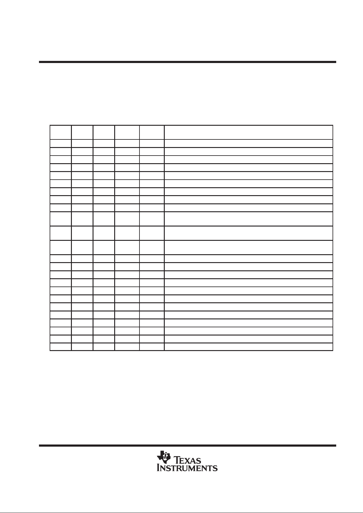
analog input channel selection
The analog input channels of the THS10064 can be selected via bits 3 to 7 of control register 0. One single
channel (single-ended or differential) is selected via bit 3 and bit 4 of control register 0. Bit 5 controls the
selection between single-ended and differential configuration. Bit 6 and bit 7 select the autoscan mode, if more
than one input channel is selected. Table 10 shows the possible selections.
Table 10. Analog Input Channel Configurations
BIT 7
SCAN
BIT 6
DIFF1
BIT 5
DIFF0
BIT 4
CHSEL1
BIT 3
CHSEL0
DESCRIPTION OF THE SELECTED INPUTS
0 0 0 0 0 Analog input AINP (single ended)
0 0 0 0 1 Analog input AINM (single ended)
0 0 0 1 0 Analog input BINP (single ended)
0 0 0 1 1 Analog input BINM (single ended)
0 0 1 0 0 Differential channel (AINP–AINM)
0 0 1 0 1 Differential channel (BINP–BINM)
1 0 0 0 1 Autoscan two single ended channels: AINP, AINM, AINP, …
1 0 0 1 0 Autoscan three single ended channels: AINP, AINM, BINP, AINP , …
1 0 0 1 1 Autoscan four single ended channels: AINP, AINM, BINP, BINM, AINP , …
1 0 1 0 1
Autoscan one differential channel and one single ended channel AINP,
(BINP–BINM), AINP, (BINP–BINM), …
1 0 1 1 0
Autoscan one differential channel and two single ended channel AINP,
AINM, (BINP–BINM), AINP, …
1 1 0 0 1
Autoscan two differential channels (AINP–AINM), (BINP–BINM),
(AINP–AINM), …
0 0 1 1 0 Reserved
0 0 1 1 1 Reserved
1 0 0 0 0 Reserved
1 0 1 0 0 Reserved
1 0 1 1 1 Reserved
1 1 0 0 0 Reserved
1 1 0 1 0 Reserved
1 1 0 1 1 Reserved
1 1 1 0 0 Reserved
1 1 1 0 1 Reserved
1 1 1 1 0 Reserved
1 1 1 1 1 Reserved
Page 20
THS10064
10-BIT 6 MSPS, SIMULTANEOUS SAMPLING
ANALOG-TO-DIGITAL CONVERTER
SLAS255 – DECEMBER 1999
20
POST OFFICE BOX 655303 • DALLAS, TEXAS 75265
analog input channel selection (continued)
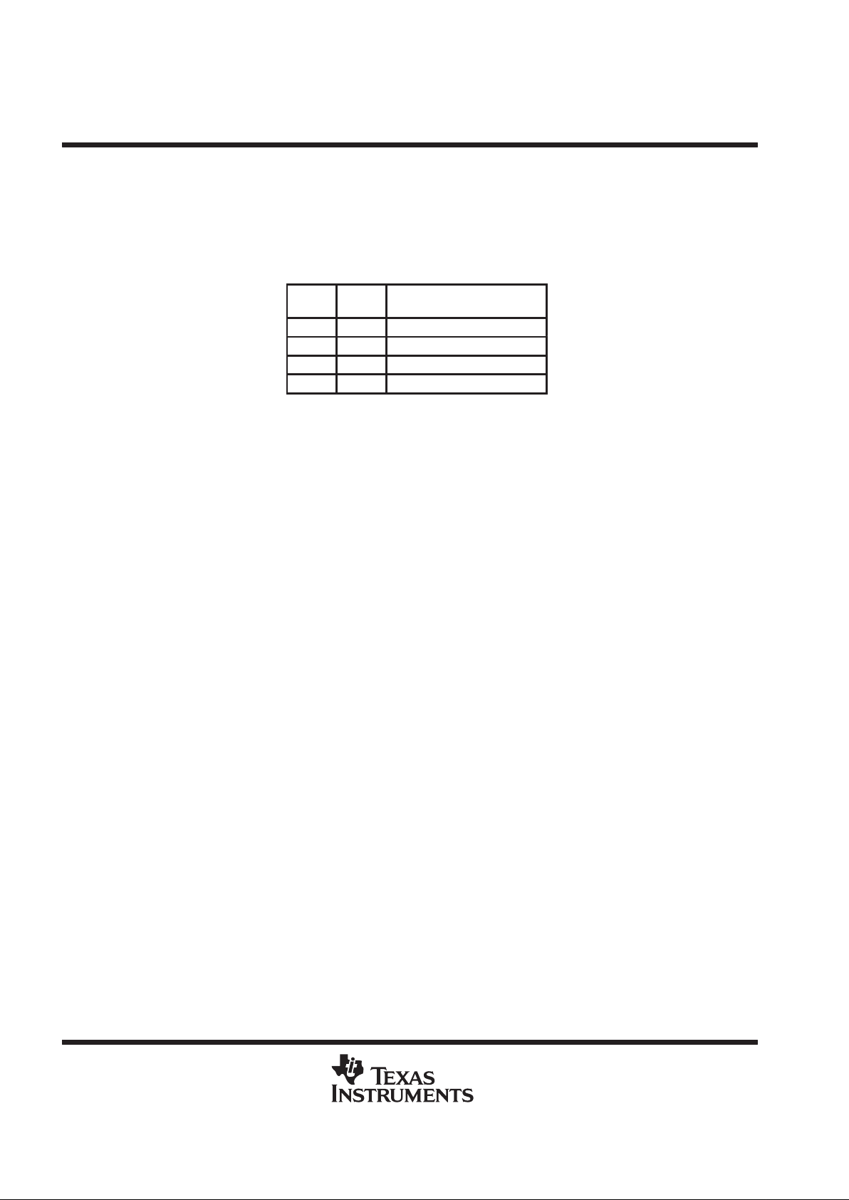
test mode
The test mode of the ADC is selected via bit 8 and bit 9 of control register 0. The different selections are shown
in Table 11.
Table 11. Test Mode
BIT 9
TEST1
BIT 8
TEST0
OUTPUT RESULT
0 0 Normal mode
0 1 V
REFP
1 0 ((V
REFM
)+(V
REFP
))/2
1 1 V
REFM
Three different options can be selected. This feature allows support testing of hardware connections between
the ADC and the processor.
Page 21
THS10064
10-BIT 6 MSPS, SIMULTANEOUS SAMPLING
ANALOG-TO-DIGITAL CONVERTER
SLAS255 – DECEMBER 1999
21
POST OFFICE BOX 655303 • DALLAS, TEXAS 75265
analog input channel selection (continued)
control register 1 (see Table 8)
– – BIT 9 BIT 8 BIT 7 BIT 6
– – RESERVED OFFSET BIN/2s R/W
BIT 5 BIT 4 BIT 3 BIT 2 BIT 1 BIT 0
DATA_P DA TA_T TRIG1 TRIG0 OVFL/FRST RESET
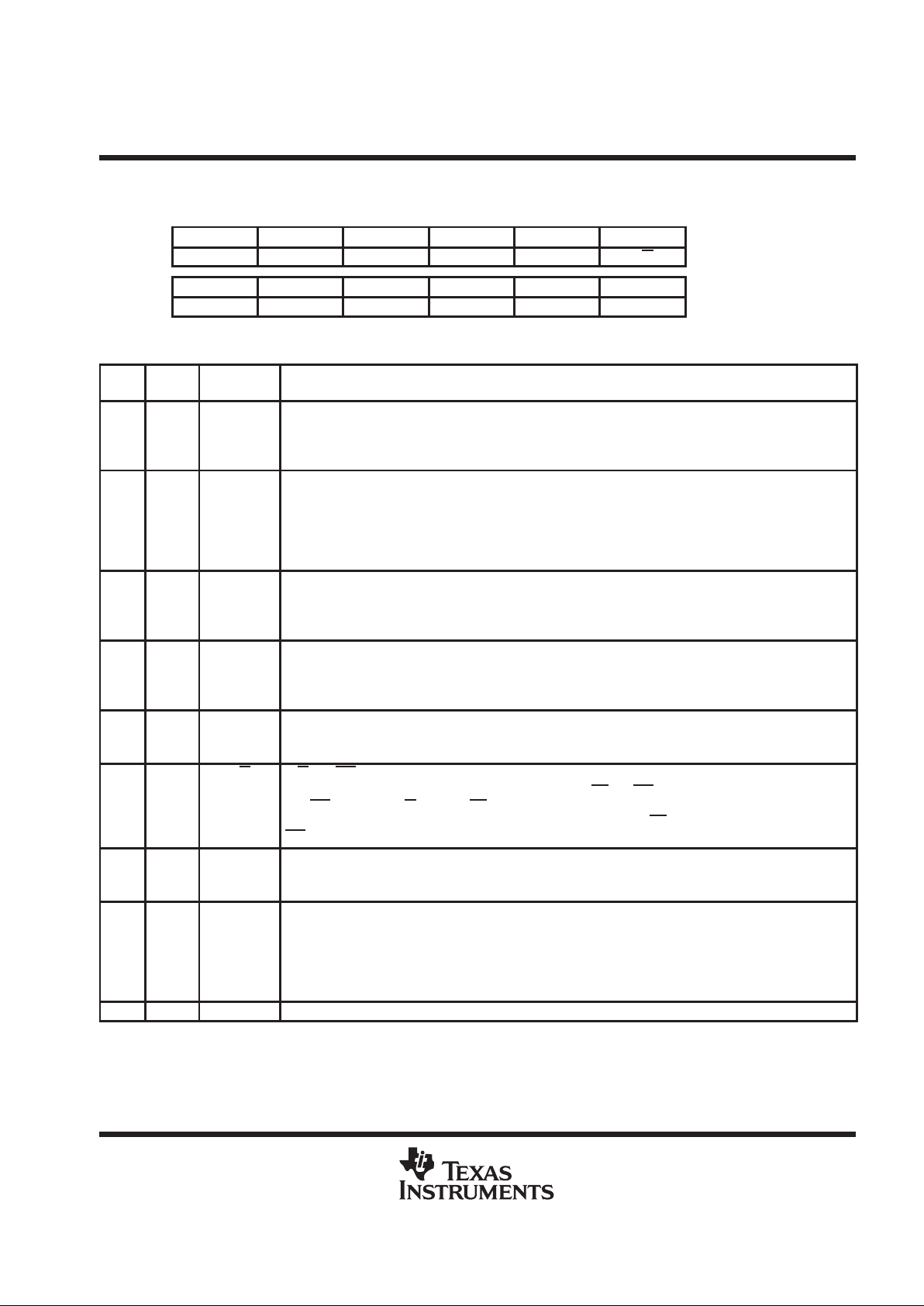
Table 12. Control Register 1 Bit Functions
BITS
RESET
VALUE
NAME FUNCTION
0 0 RESET Reset
Writing a 1 into this bit resets the device and sets the control register 0 and control register 1 to the reset
values. In addition the FIFO pointer and of fset register is reset. After reset, it takes 5 clock cycles until the first
value is converted and written into the FIFO.
1 0 OVFL
(read only)
FRST
(write only)
Overflow flag (read only)
Bit 1 of control register 1 indicates an overflow in the FIFO.
Bit 1 = 0 → no overflow occurred.
Bit 1 = 1 → an overflow occurred. This bit is reset to 0, after this control register is read from the processor.
FRST: FIFO reset (write only)
By writing a 1 into this bit, the FIFO is reset.
2, 3 0,0 F0, F1 FIFO trigger level
Bit 2 and bit 3 of control register 1 are used to set the trigger level for the FIFO. If the trigger level is reached,
the signal DAT A_A V (data available) becomes active according to the settings of DATA_T and DA T A_P. This
indicates to the processor that the ADC values can be read. Refer to Table 13.
4 1 DATA_T DATA_AV type
Bit 4 of control register 1 controls whether the DATA_AV signal is a pulse or static (e.g for edge or level
sensitive interrupt inputs). If it is set to 0, the DAT A_AV signal is static. If it is set to 1, the DAT A_A V signal is a
pulse. Refer to Table 14.
5 1 DATA_P DA TA_AV polarity
Bit 5 of control register 1 controls the polarity of DAT A_AV . If it is set to 1, DA TA_A V is active high. If it is set to 0,
DATA_AV is active low. Refer to Table 14.
6 0 R/W R/W, RD/WR selection
Bit 6 of control register 1 controls the function of the inputs RD
and WR. When bit 6 in control register 1 is set
to 1, WR
becomes a R/W input and RD is disabled. From now on a read is signalled with R/W high and a write
with R/W as a low signal. If bit 6 in control register 1 is set to 0, the input RD
becomes a read input and the input
WR
becomes a write input.
7 0 BIN/2s Complement select
If bit 7 of control register 1 is set to 0, the output value of the ADC is in twos complement. If bit 7 of
control register 1 is set to 1, the output value of the ADC is in binary format. Refer to T able 3 through Table 6.
8 0 OFFSET Offset cancellation mode
Bit 8 = 0 → normal conversion mode
Bit 8 = 1 → offset calibration mode
If a 1 is written into bit 8 of control register 1, the device internally sets the inputs to zero and does a conversion. The conversion result is stored in an offset register and subtracted from all conversions in order
to reduce the offset error.
9 0 RESERVED Always write 0.
Page 22
THS10064
10-BIT 6 MSPS, SIMULTANEOUS SAMPLING
ANALOG-TO-DIGITAL CONVERTER
SLAS255 – DECEMBER 1999
22
POST OFFICE BOX 655303 • DALLAS, TEXAS 75265
FIFO trigger level
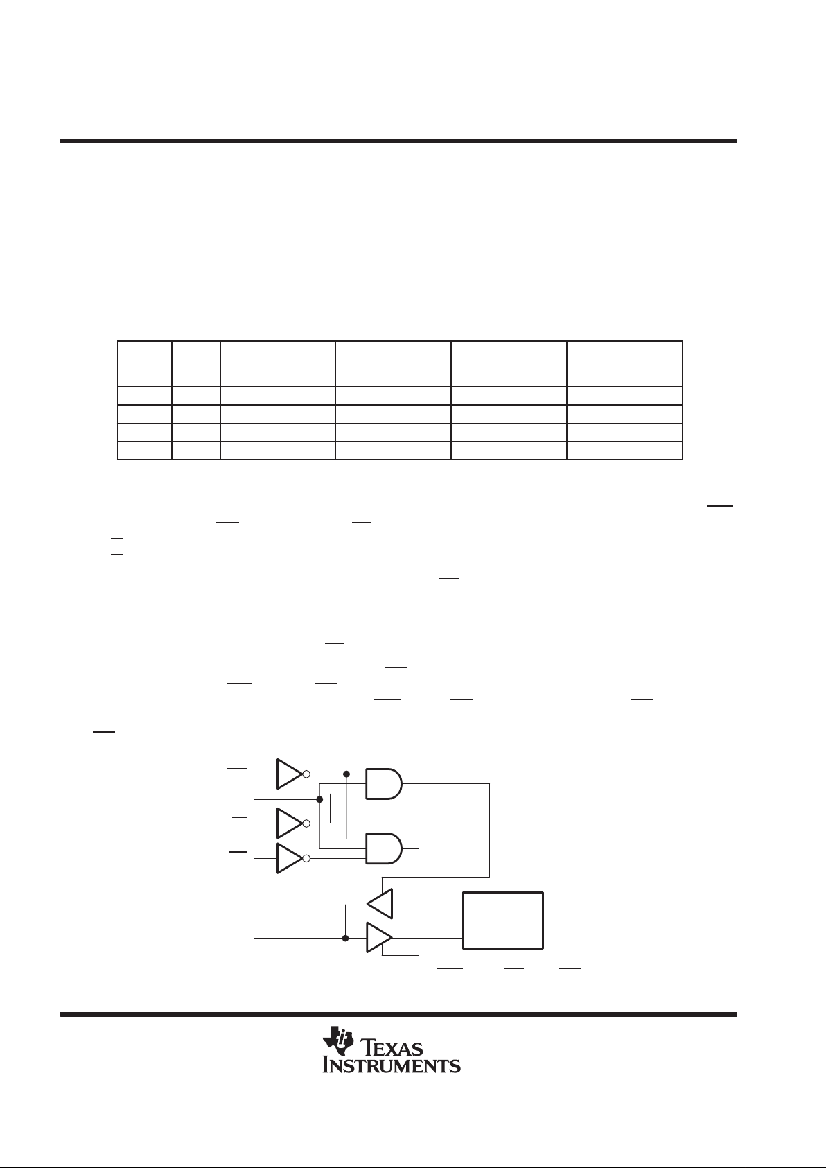
Bit 2 and bit 3 (TRIG1, TRIG0) of control register 1 are used to set the trigger level of the FIFO (see Table 13).
If the trigger level is reached, the DA TA_AV (data available) signal becomes active according to the setting of
the signal DATA_AV to indicate to the processor that the ADC values can be read.
T able 13 shows four different programmable trigger levels for each configuration. The FIFO trigger level, which
can be selected, is dependent on the number of input channels. Both, a differential or a single-ended input is
considered as one channel. The processor therefore always reads the data from the FIFO in the same order
and is able to distinguish between the channels.
Table 13. FIFO Trigger Level
BIT 3
TRIG1
BIT 2
TRIG0
TRIGGER LEVEL
FOR 1 CHANNEL
(ADC values)
TRIGGER LEVEL
FOR 2 CHANNELS
(ADC values)
TRIGGER LEVEL
FOR 3 CHANNEL
(ADC values)
TRIGGER LEVEL
FOR 4 CHANNELS
(ADC values)
0 0 01 02 03 04
0 1 04 04 06 08
1 0 08 08 09 12
1 1 14 12 12 Reserved
Timing and Signal Description of the THS10064
The reading from the THS10064 and writing to the THS10064 is perfomed by using the chip select inputs (CS0,
CS1), the write input WR and the read input RD. The write input is configurable to a combined read/write input
(R/W
). This is desired in cases where the connected processor consists of a combined read/write ouput signal
(R/W). The two chip select inputs can be used to interface easily to a processor.
Reading from the THS10064 takes place by an internal RD
int
signal, which is generated from the logical
combination of the external signals CS0
, CS1 and RD (see Figure 12). This signal is then used to strobe the
words out of the FIFO and to enable the output buffers. The last external signal (either CS0, CS1 or RD) to
become valid will make RD
int
active while the write input (WR) is inactive. The first of those external signals going
to its inactive state will then deactivate RD
int
again.
Writing to the THS10064 takes place by an internal WR
int
signal, which is generated from the logical combination
of the external signals CS0, CS1 and WR. This signal is then used to strobe the control words into the control
registers 0 and 1. The last external signal (either CS0
, CS1 or WR) to become valid will make WR
int
active while
the read input (RD) is inactive. The first of those external signals going to its inactive state will then deactivate
WR
int
again.
Read Enable
Write Enable
Control/Data
Registers
CS0
CS1
RD
WR
Data Bits
Figure 12. Logical Combination of CS0, CS1, RD, and WR
Page 23
THS10064
10-BIT 6 MSPS, SIMULTANEOUS SAMPLING
ANALOG-TO-DIGITAL CONVERTER
SLAS255 – DECEMBER 1999
23
POST OFFICE BOX 655303 • DALLAS, TEXAS 75265
DATA_AV type
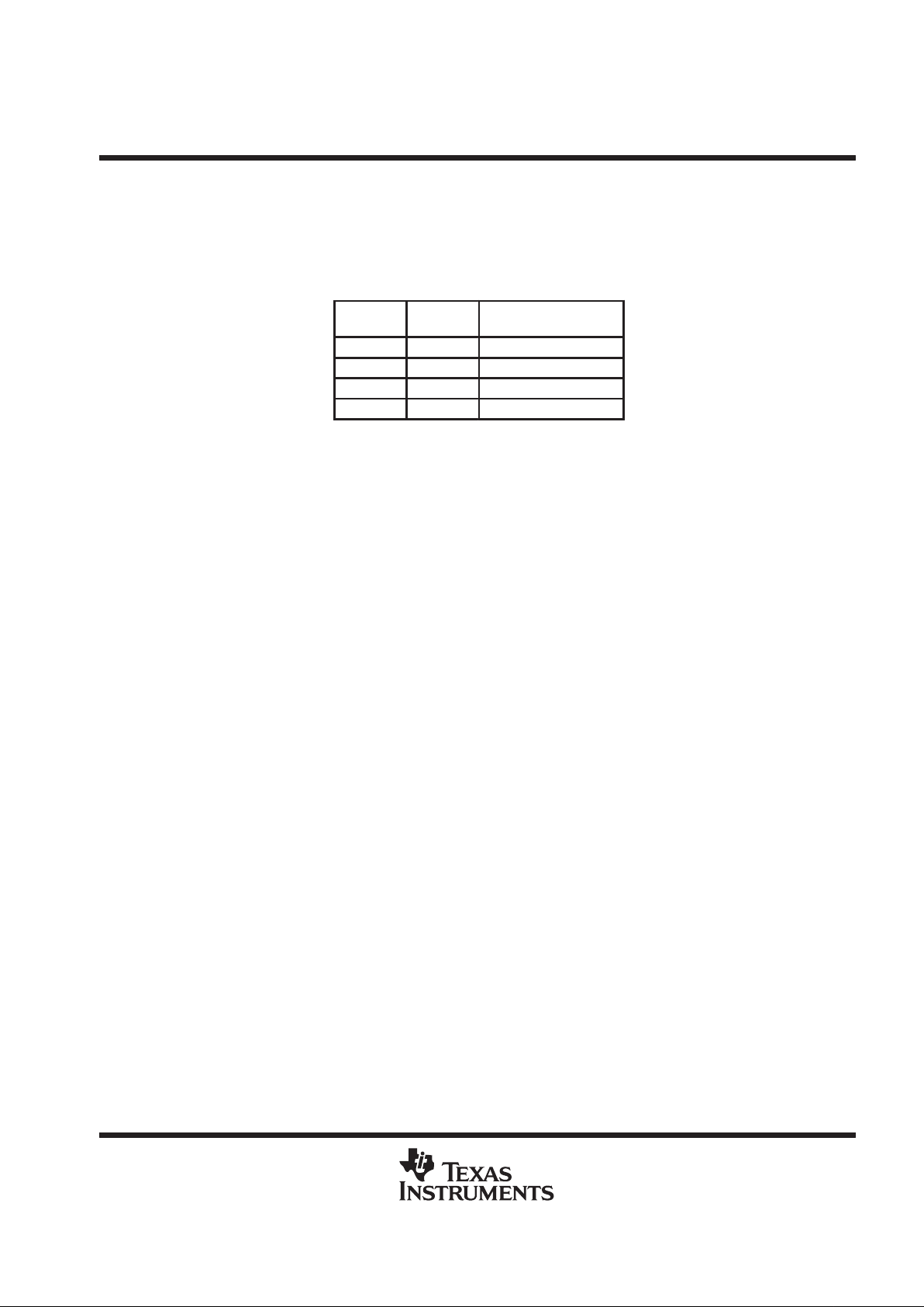
Bit 4 and bit 5 (DATA_T, DATA_P) of control register 1 are used to program the signal DATA_AV. Bit 4 of
control register 1 determines whether the DATA_AV signal is static or a pulse. Bit 5 of the control register
determines the polarity of DATA_AV. This is shown in Table 14.
Table 14. DATA_AV Type
BIT 5
DATA_P
BIT 4
DATA_T
DATA_AV TYPE
0 0 Active low level
0 1 Active low pulse
1 0 Active high level
1 1 Active high pulse
The signal DA TA_AV is set to active when the trigger condition is satisified. It is set back inactive independent
of the DATA_T selection (pulse or level).
If level mode is chosen, DA TA_A V is set inactive after the first of the TL (TL = trigger level) reads (with the falling
edge of READ). The trigger condition is checked again after TL reads.
If pulse mode is chosen, the signal DATA_AV is a pulse with a width of one half of a CONV_CLK cycle in
continuous conversion mode and one half of a clock cycle of the internal oscillator in single conversion mode.
The next DA TA_AV pulse (when the trigger condition is satisfied) is sent out the earliest, when the TL values,
written into the FIFO before, were read out by the processor.
Page 24
THS10064
10-BIT 6 MSPS, SIMULTANEOUS SAMPLING
ANALOG-TO-DIGITAL CONVERTER
SLAS255 – DECEMBER 1999
24
POST OFFICE BOX 655303 • DALLAS, TEXAS 75265
timing and signal description of the THS10064
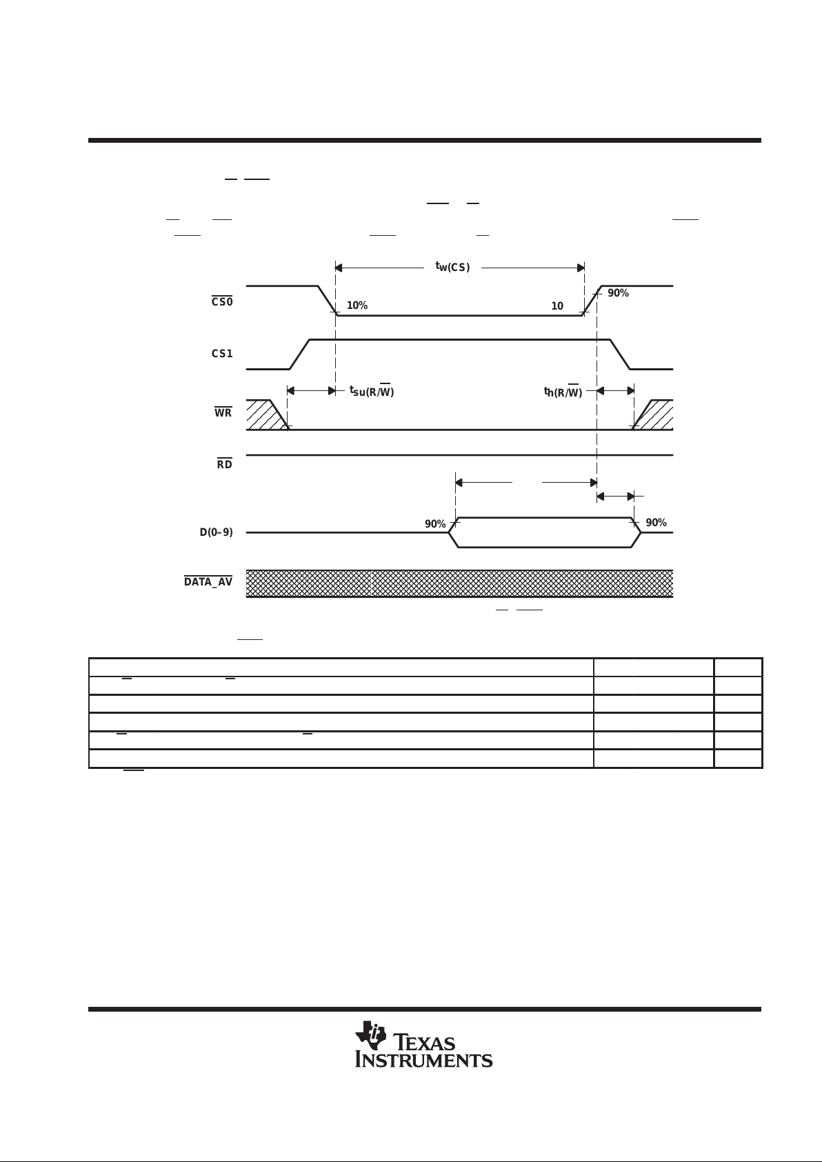
read timing (using R/W, CS0-controlled)
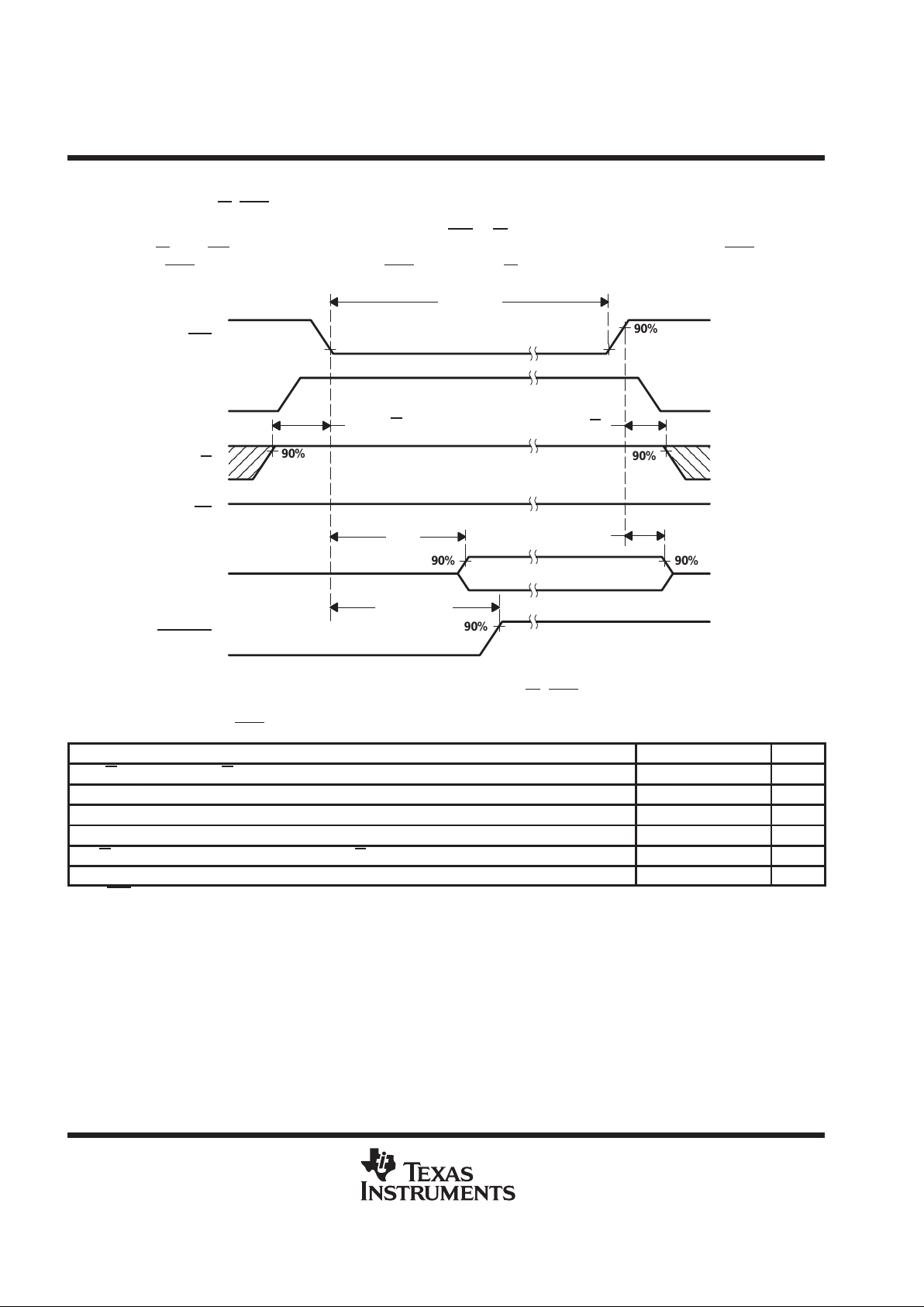
Figure 13 shows the read-timing behavior when the WR(R/W) input is programmed as a combined read-write
input R/W. The RD input has to be tied to high-level in this configuration. This timing is called CS0-controlled
because CS0 is the last external signal of CS0, CS1, and R/W which becomes valid.
90%90%
90%
90%
90%
90%
10%
10%
t
w(CS)
t
su(R/W
)
t
h(R/W)
t
a
t
h
t
d(CSDAV)
CS0
CS1
R/W
RD
D(0–9)
DATA_AV
Figure 13. Read Timing Diagram Using R/W (CS0-controlled)
read timing parameter (CS0-controlled)
†
PARAMETER MIN TYP MAX UNIT
t
su(R/W)
Setup time, R/W high to last CS valid 0 ns
t
a
Access time, last CS valid to data valid 0 10 ns
t
d(CSDAV)
Delay time, last CS valid to DATA_AV inactive 12 ns
t
h
Hold time, first CS invalid to data invalid 0 5 ns
t
h(R/W)
Hold time, first external CS invalid to R/W change 5 ns
t
w(CS)
Pulse duration, CS active 10 ns
†
CS = CS0
Page 25
THS10064
10-BIT 6 MSPS, SIMULTANEOUS SAMPLING
ANALOG-TO-DIGITAL CONVERTER
SLAS255 – DECEMBER 1999
25
POST OFFICE BOX 655303 • DALLAS, TEXAS 75265
timing and signal description of the THS10064 (continued)
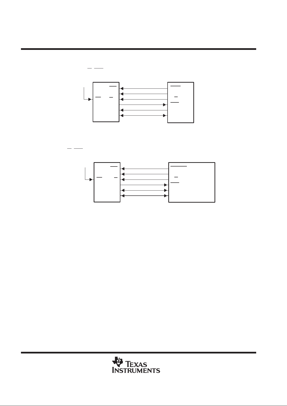
write timing (using R/W, CS0-controlled)
Figure 14 shows the write-timing behavior when the WR(R/W) input is programmed as a combined read-write
input R/W. The RD input has to be tied to high-level in this configuration. This timing is called CS0-controlled
because CS0 is the last external signal of CS0, CS1, and R/W which becomes valid.
90%
90%
90%
10%
t
w(CS)
t
su(R/W
)
t
h(R/W)
CS0
CS1
WR
RD
D(0–9)
DATA_AV
10%
t
su
t
h
Figure 14. Write Timing Diagram Using R/W (CS0-controlled)
read timing parameter (CS0-controlled)
†
PARAMETER MIN TYP MAX UNIT
t
su(R/W
)
Setup time, R/W stable to last CS valid 0 ns
t
su
Setup time, data valid to first CS invalid 5 ns
t
h
Hold time, first CS invalid to data invalid 5 ns
t
h(R/W)
Hold time, first CS invalid to R/W change 5 ns
t
w(CS)
Pulse duration, CS active 10 ns
†
CS = CS0
Page 26
THS10064
10-BIT 6 MSPS, SIMULTANEOUS SAMPLING
ANALOG-TO-DIGITAL CONVERTER
SLAS255 – DECEMBER 1999
26
POST OFFICE BOX 655303 • DALLAS, TEXAS 75265
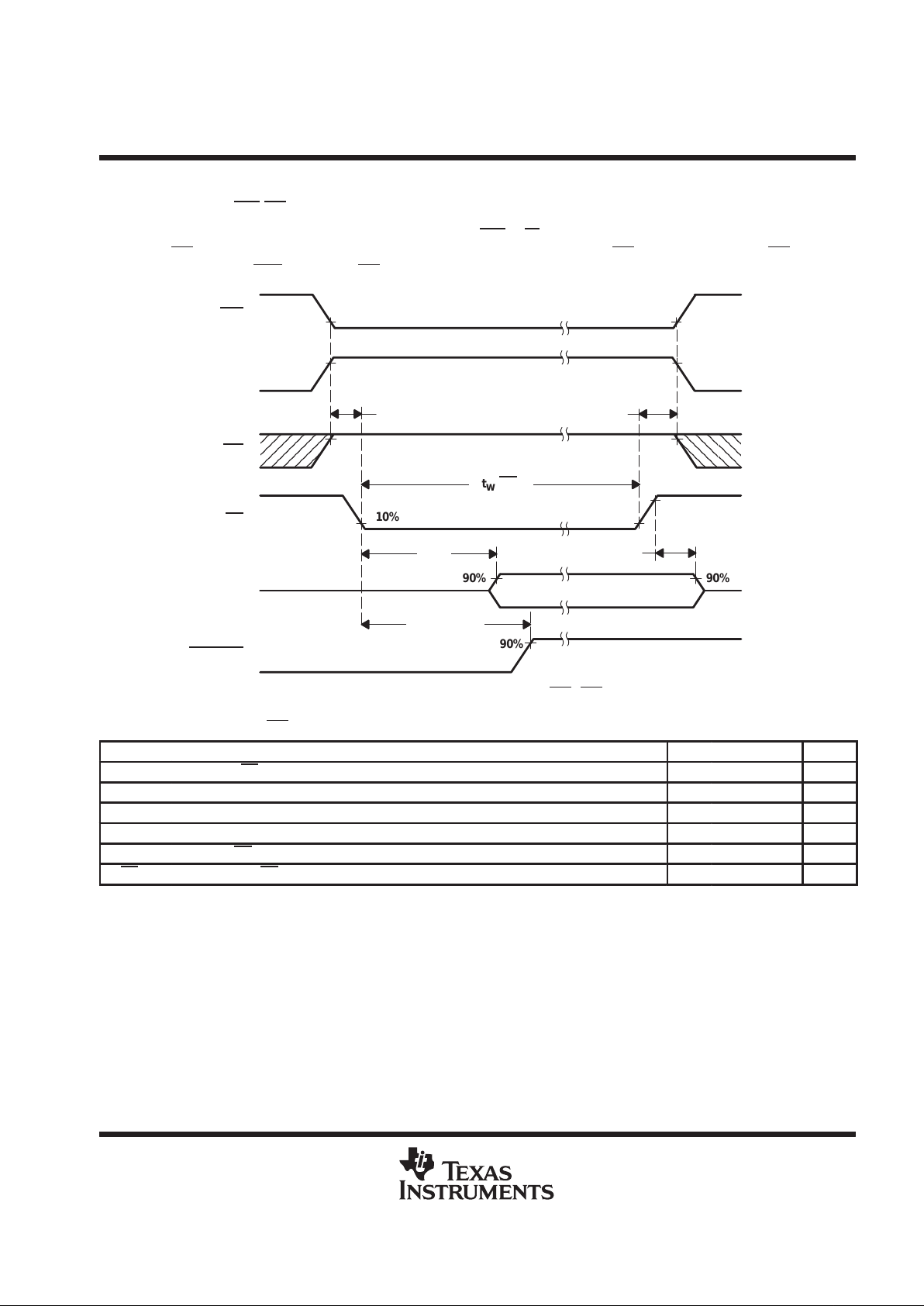
interfacing the THS10064 to the TMS320C30/31/33 DSP
The following application circuit shows an interface of the THS10064 to the TMS320C30/31/33 DSPs. The read
and write timings (using R/W, CS0-controlled) shown before are valid for this specific interface.
CS0
CS1
R/
W
DATA_AV
CONV_CLK
DATA
RD
DV
DD
THS10064 TMS320C30/31/33
STRB
A23
R/W
INTX
TOUT
DATA
interfacing the THS10064 to the TMS320C54x using I/O strobe
The following application circuit shows an interface of the THS10064 to the TMS320C54x. The read and write
timings (using R/W
, CS0-controlled) shown before are valid for this specific interface.
CS0
CS1
R/W
DATA_AV
CONV_CLK
DATA
RD
DV
DD
THS10064 TMS320C54x
I/O STRB
A15
R/W
INTX
BCLK
DATA
Page 27
THS10064
10-BIT 6 MSPS, SIMULTANEOUS SAMPLING
ANALOG-TO-DIGITAL CONVERTER
SLAS255 – DECEMBER 1999
27
POST OFFICE BOX 655303 • DALLAS, TEXAS 75265
timing and signal description of the THS10064 (continued)
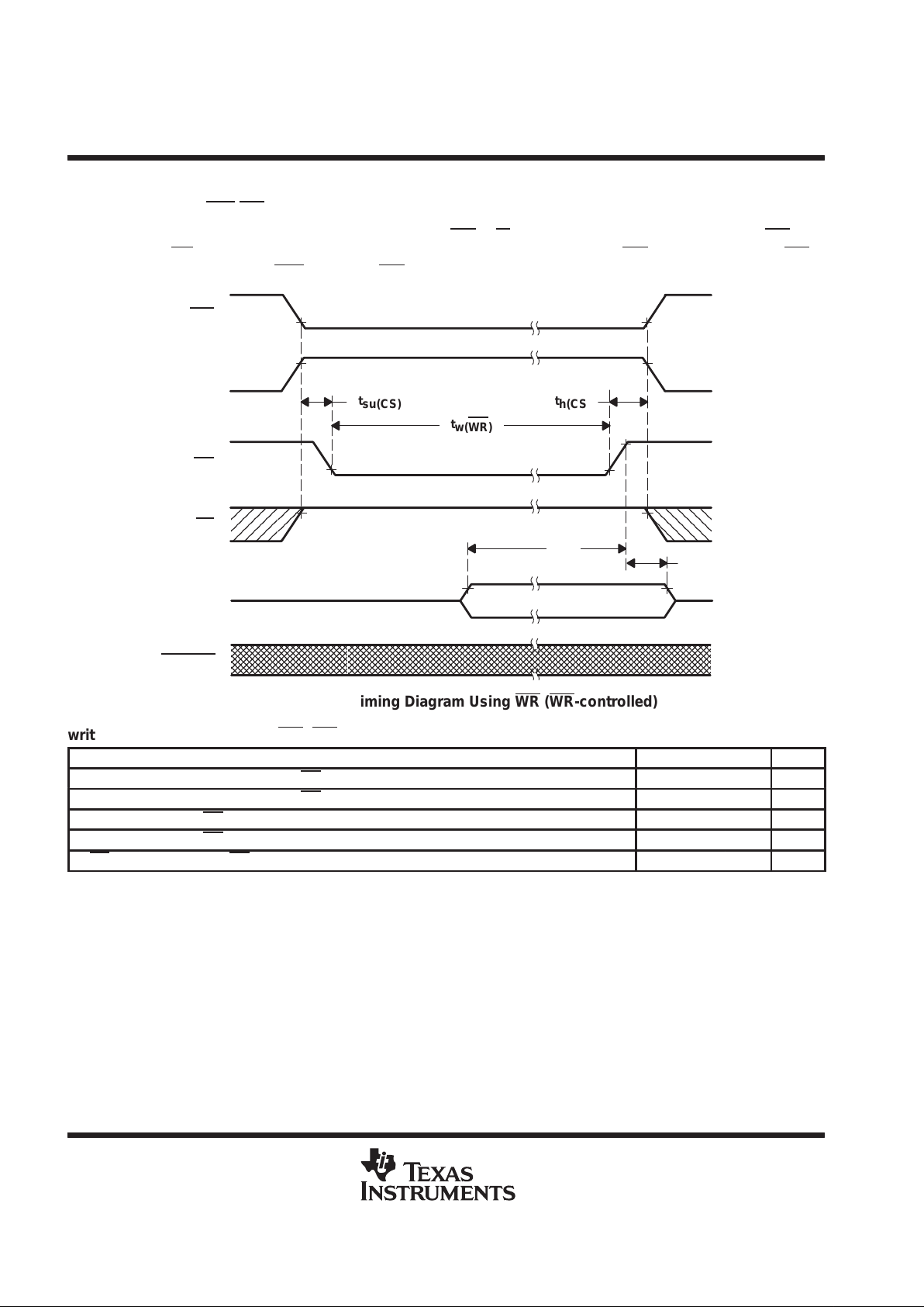
read timing (using RD, RD-controlled)
Figure 15 shows the read-timing behavior when the WR(R/W) input is programmed as a write-input only . The
input RD acts as the read-input in this configuration. This timing is called RD-controlled because RD is the last
external signal of CS0, CS1, and RD which becomes valid.
90%90%
90%
10%
t
w(RD
)
t
su(CS)
t
h(CS)
t
a
t
h
t
d(CSDAV)
CS0
CS1
WR
RD
D(0–9)
DATA_AV
10%
Figure 15. Read Timing Diagram Using RD (RD-controlled)
read timing parameter (RD-controlled)
PARAMETER MIN TYP MAX UNIT
t
su(CS)
Setup time, RD low to last CS valid 0 ns
t
a
Access time, last CS valid to data valid 0 10 ns
t
d(CSDAV)
Delay time, last CS valid to DATA_AV inactive 12 ns
t
h
Hold time, first CS invalid to data invalid 0 5 ns
t
h(CS)
Hold time, RD change to first CS invalid 5 ns
t
w(RD)
Pulse duration, RD active 10 ns
Page 28
THS10064
10-BIT 6 MSPS, SIMULTANEOUS SAMPLING
ANALOG-TO-DIGITAL CONVERTER
SLAS255 – DECEMBER 1999
28
POST OFFICE BOX 655303 • DALLAS, TEXAS 75265
timing and signal description of the THS10064 (continued)
write timing (using WR, WR-controlled)
Figure 16 shows the write-timing behavior when the WR(R/W) input is programmed as a write input WR only .
The input RD acts as the read input in this configuration. This timing is called WR-controlled because WR is
the last external signal of CS0, CS1, and WR which becomes valid.
90%90%
10%
t
su
t
h
D(0–9)
DATA_AV
10%
t
w(WR)
t
su(CS)
t
h(CS)
CS0
CS1
WR
RD
МММММММММММММММММММММ
Figure 16. Write Timing Diagram Using WR (WR-controlled)
write timing parameter using WR (WR-controlled)
PARAMETER MIN TYP MAX UNIT
t
su(CS)
Setup time, CS stable to last WR valid 0 ns
t
su
Setup time, data valid to first WR invalid 5 ns
t
h
Hold time, WR invalid to data invalid 5 ns
t
h(CS)
Hold time, WR invalid to CS change 5 ns
t
w(WR)
Pulse duration, WR active 10 ns
Page 29
THS10064
10-BIT 6 MSPS, SIMULTANEOUS SAMPLING
ANALOG-TO-DIGITAL CONVERTER
SLAS255 – DECEMBER 1999
29
POST OFFICE BOX 655303 • DALLAS, TEXAS 75265
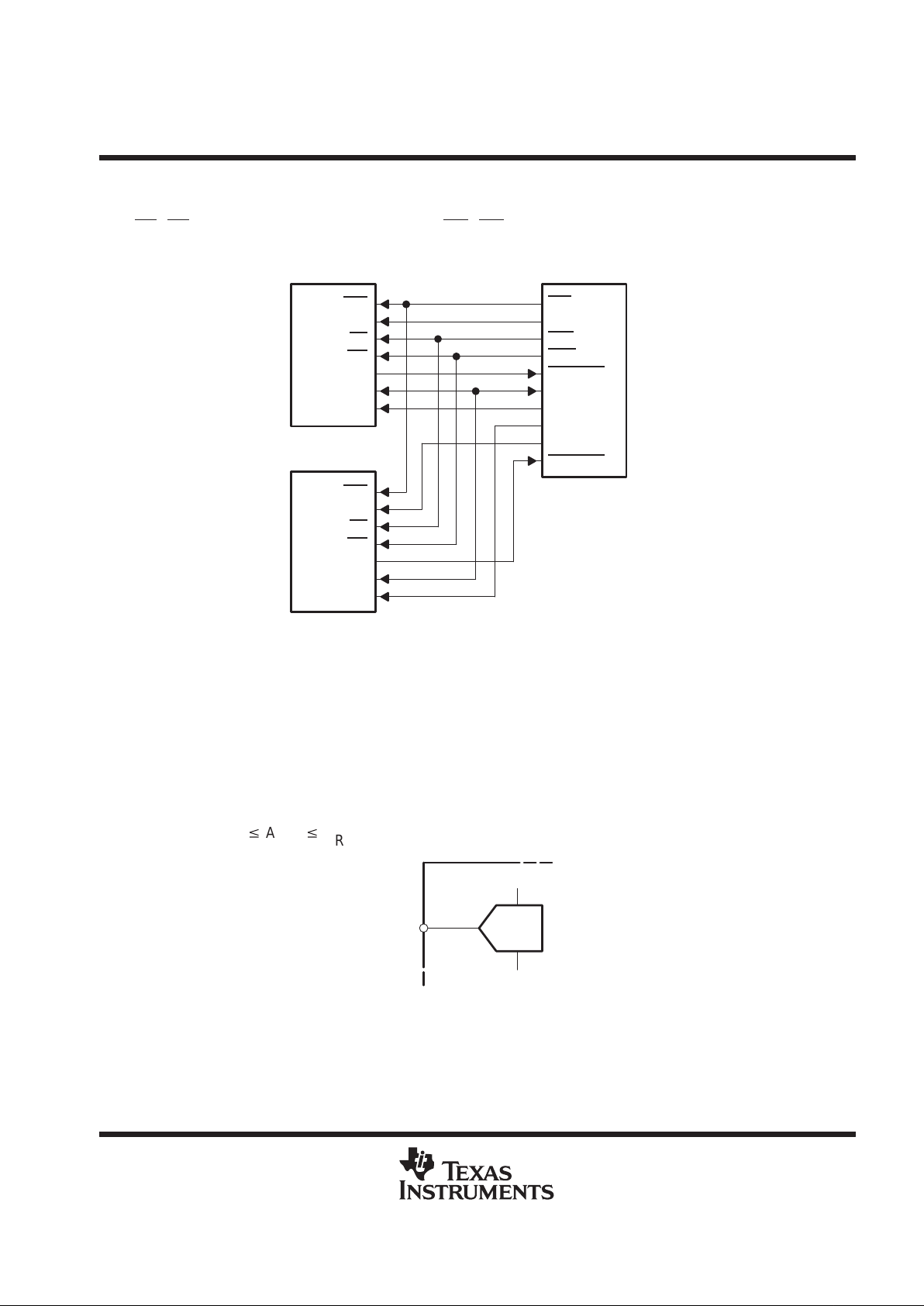
interfacing the THS10064 to the TMS320C6201 DSP
The following application circuit shows an interface of the THS10064 to the TMS320C6201. The read (using
RD, RD-controlled) and write timings (using WR, WR-controlled) shown before are valid for this specific
interface.
CS0
CS1
RD
WR
DATA_AV
DATA
CONV_CLK
THS10064–1
CS0
CS1
RD
WR
DATA_AV
DATA
CONV_CLK
THS10064–2
TMS320C6201
CE1
EA20
ARE
AWE
EXT_INT6
DATA
TOUT1
TOUT2
EA21
EXT_INT7
analog input configuration and reference voltage
The THS10064 features four analog input channels. These can be configured for either single-ended or
differential operation. Best performance is achieved in differential mode. Figure 17 shows a simplified model,
where a single-ended configuration for channel AINP is selected. The reference voltages for the ADC itself are
V
REFP
and V
REFM
(either internal or exteral reference voltage). The analog input voltage range goes from V
REFM
to V
REFP
. This means that V
REFM
defines the minimum voltage, which can be applied to the ADC. V
REFP
defines
the maximum voltage, which can be applied to the ADC. The internal reference source provides the voltage
V
REFM
of 1.5 V and the voltage V
REFP
of 3.5 V . The resulting analog input voltage swing of 2 V can be expressed
by:
V
REFM
v
AINPvV
REFP
10-Bit
ADC
V
REFP
V
REFM
AINP
Figure 17. Single-Ended Input Stage
(1)
Page 30
THS10064
10-BIT 6 MSPS, SIMULTANEOUS SAMPLING
ANALOG-TO-DIGITAL CONVERTER
SLAS255 – DECEMBER 1999
30
POST OFFICE BOX 655303 • DALLAS, TEXAS 75265
analog input configuration and reference voltage (continued)
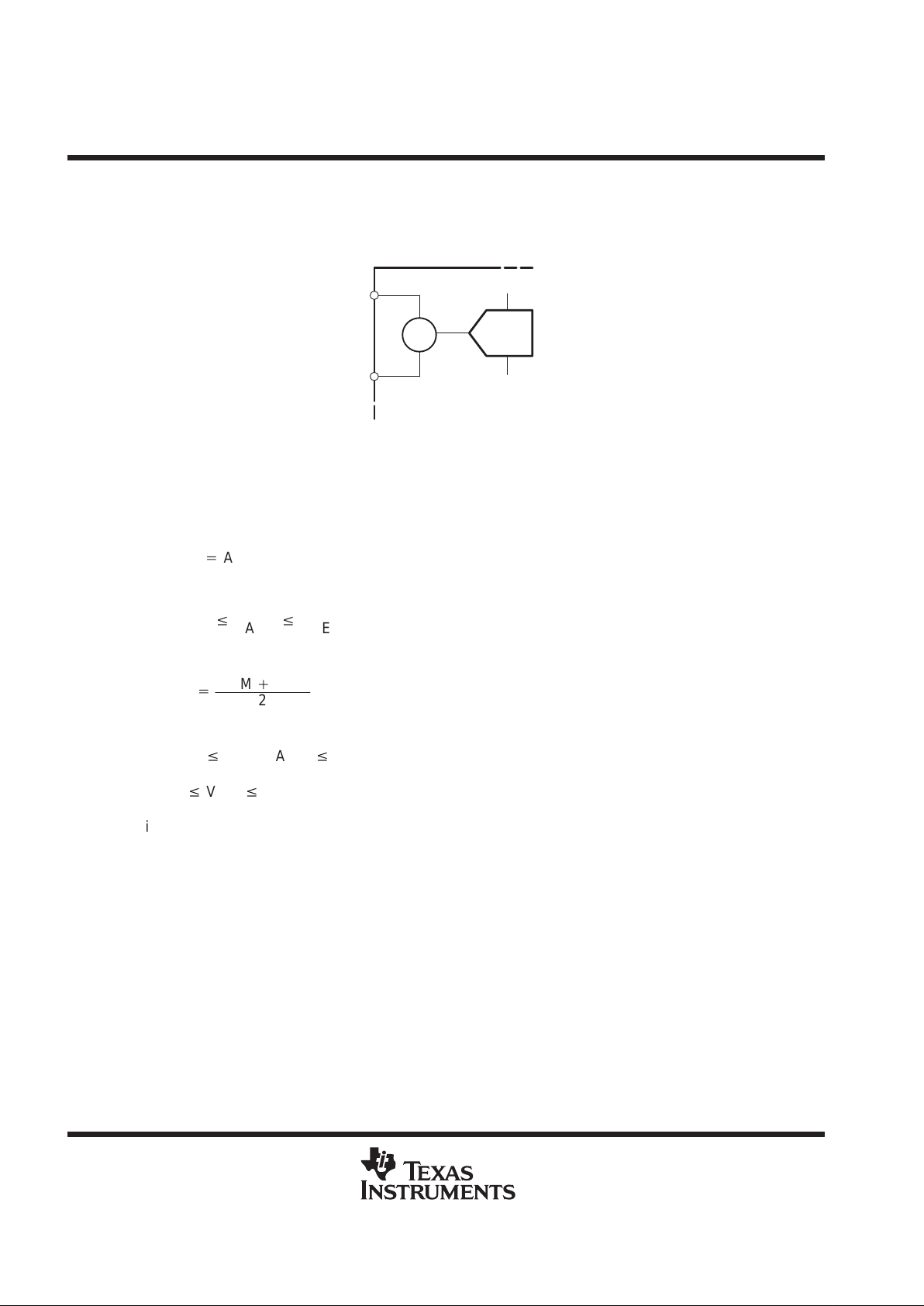
A differential operation is desired for many applications. Figure 18 shows a simplified model for the analog inputs
AINM and AINP , which are configured for differential operation. This configuration has a few advantages, which
are discussed in the following paragraphs.
10-Bit
ADC
V
REFP
V
REFM
AINP
Σ
V
ADC
AINM
+
–
Figure 18. Differential Input Stage
In comparison to the single-ended configuration it can be seen that the voltage, V
ADC
, which is applied at the
input of the ADC is the difference between the input AINP and AINM. This means that V
REFM
defines the
minimum voltage (V
ADC
) which can be applied to the ADC. V
REFP
defines the maximum voltage (V ADC) which
can be applied to the ADC. The voltage V
ADC
can be calculated as follows:
V
ADC
+
ABS(AINP–AINM
)
The voltage V
ADC
has to satisfy the following condition:
V
REFM
v
V
ADC
v
V
REFP
An advantage to single-ended operation is that the common-mode voltage
VCM+
AINM)AINP
2
can be rejected in the differential configuration, if the following condition for the analog input voltages is true:
AGNDvAINM, AINPvAV
DD
1VvVCMv
4V
In addition to the common-mode voltage rejection, the differential operation allows a dc-offset rejection which
is common to both analog inputs. See also Figure 20.
single-ended mode of operation
The THS10064 can be configured for single-ended operation using dc or ac coupling. In either case, the input
of the THS10064 must be driven from an operational amplifier that does not degrade the ADC performance.
Because the THS10064 operates from a 5-V single supply, it is necessary to level-shift ground-based bipolar
signals to comply with its input requirements. This can be achieved with dc and ac coupling. An application
example is shown for dc-coupled level shifting in the following section, dc coupling.
(2)
(3)
(4)
(5)
(6)
Page 31
THS10064
10-BIT 6 MSPS, SIMULTANEOUS SAMPLING
ANALOG-TO-DIGITAL CONVERTER
SLAS255 – DECEMBER 1999
31
POST OFFICE BOX 655303 • DALLAS, TEXAS 75265
dc coupling
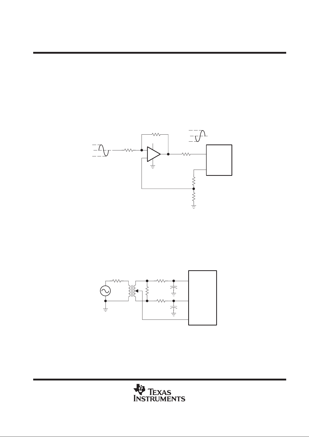
An operational amplifier can be configured to shift the signal level according to the analog input voltage range
of the THS10064. The analog input voltage range of the THS10064 goes from 1.5 V to 3.5 V. An op-amp
specified for 5-V single supply can be used as shown in Figure 19.
Figure 19 shows an application example where the analog input signal in the range from –1 V up to 1 V is shifted
by an op-amp to the analog input range of the THS10064 (1.5 V to 3.5 V). The op-amp is configured as an
inverting amplifier with a gain of –1. The required dc voltage of 1.25 V at the noninverting input is derived from
the 2.5-V output reference REFOUT of the THS10064 by using a resistor divider. Therefore, the op-amp output
voltage is centered at 2.5 V. The use of ratio matched, thin-film resistor networks minimizes gain and offset
errors.
_
+
5 V
R
R
R
S
3.5 V
2.5 V
1.5 V
THS10064
AINP
REFOUT
R
R
1.25 V
1 V
0 V
–1 V
Figure 19. Level-Shift for DC-Coupled Input
differential mode of operation
For the differential mode of operation, a conversion from single-ended to differential is required. A conversion
to differential signals can be achieved by using an RF-transformer, which provides a center tap. Best
performance is achieved in differential mode.
THS10064
AINP
AINM
REFOUT
C
C
R
R
200 Ω
49.9 Ω
Mini Circuits
T4–1
Figure 20. Transformer Coupled Input
Page 32
THS10064
10-BIT 6 MSPS, SIMULTANEOUS SAMPLING
ANALOG-TO-DIGITAL CONVERTER
SLAS255 – DECEMBER 1999
32
POST OFFICE BOX 655303 • DALLAS, TEXAS 75265
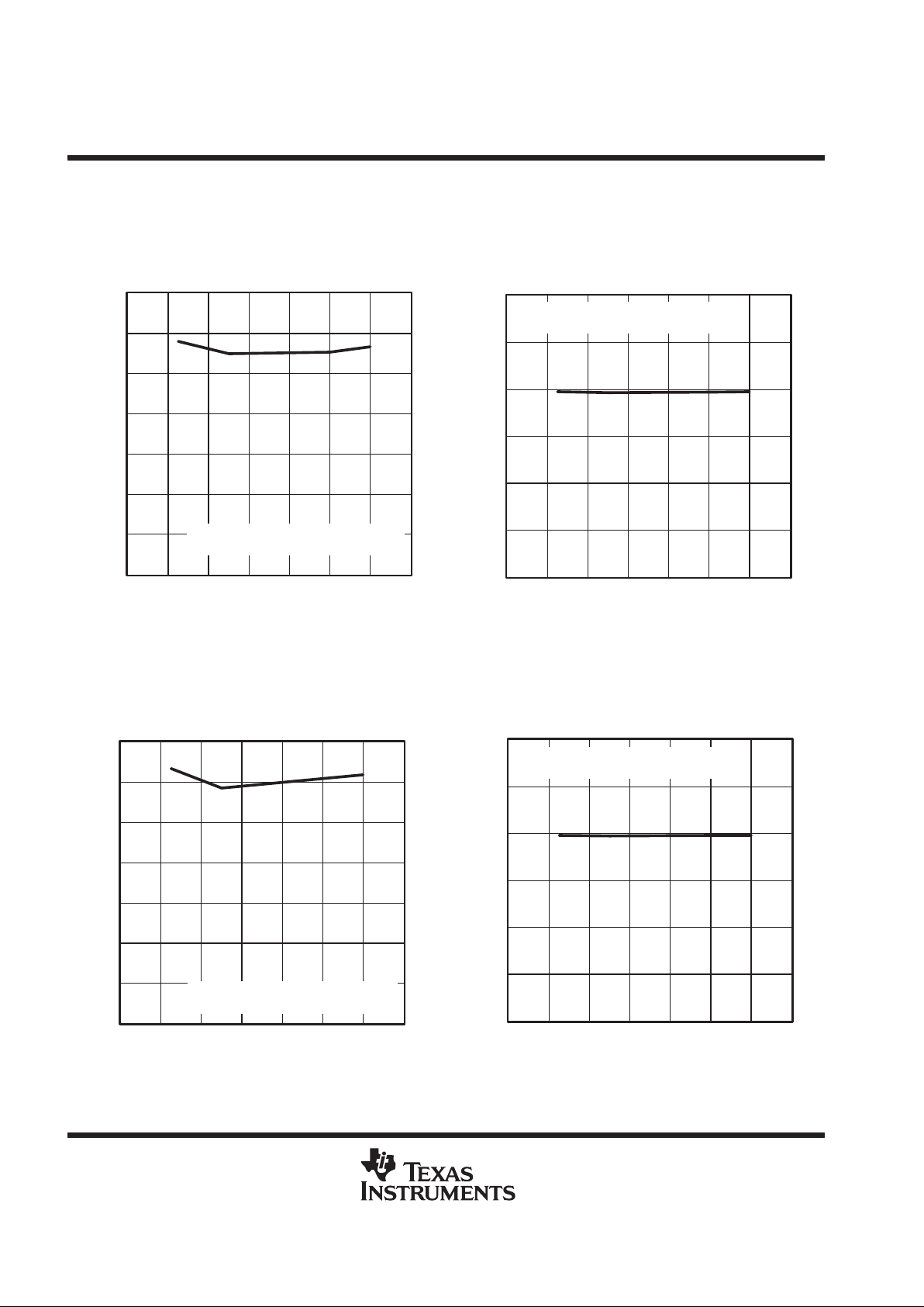
TYPICAL CHARACTERISTICS
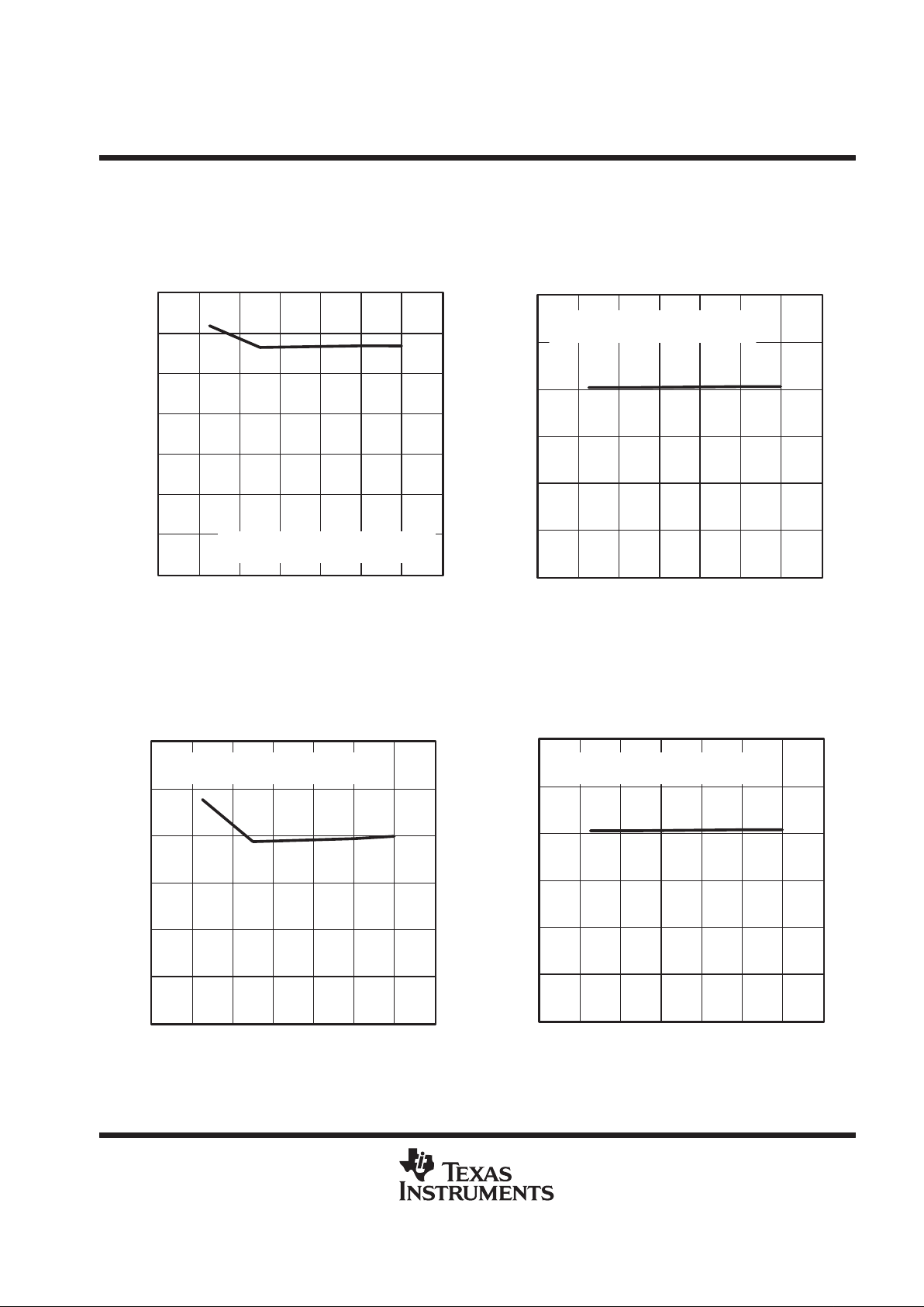
Figure 21
20
30
40
50
60
70
80
90
01234567
TOTAL HARMONIC DISTORTION
vs
SAMPLING FREQUENCY (SINGLE-ENDED)
AVDD = 5 V, DVDD = BVDD = 3 V,
fIN = 500 kHz, AIN = –0.5 dB FS
fs – Sampling Frequency – MHz
THD – Total Harmonic Distortion – dB
Figure 22
20
30
40
50
60
70
80
01234567
SIGNAL-TO-NOISE AND DISTORTION
vs
SAMPLING FREQUENCY (SINGLE-ENDED)
fs – Sampling Frequency – MHz
SINAD – Signal-to-Noise and Distortion – dB
AVDD = 5 V, DVDD = BVDD = 3 V,
fIN = 500 kHz, AIN = –0.5 dB FS
Figure 23
20
30
40
50
60
70
80
90
01234567
SPURIOUS FREE DYNAMIC RANGE
vs
SAMPLING FREQUENCY (SINGLE-ENDED)
fs – Sampling Frequency – MHz
SFDR – Spurious Free Dynamic Range – dB
AVDD = 5 V, DVDD = BVDD = 3 V,
fIN = 500 kHz, AIN = –0.5 dB FS
Figure 24
SIGNAL-TO-NOISE
vs
SAMPLING FREQUENCY (SINGLE-ENDED)
fs – Sampling Frequency – MHz
SNR – Signal-to-Noise – dB
20
30
40
50
60
70
80
01234567
AVDD = 5 V, DVDD = BVDD = 3 V,
fIN = 500 kHz, AIN = –0.5 dB FS
Page 33
THS10064
10-BIT 6 MSPS, SIMULTANEOUS SAMPLING
ANALOG-TO-DIGITAL CONVERTER
SLAS255 – DECEMBER 1999
33
POST OFFICE BOX 655303 • DALLAS, TEXAS 75265
TYPICAL CHARACTERISTICS
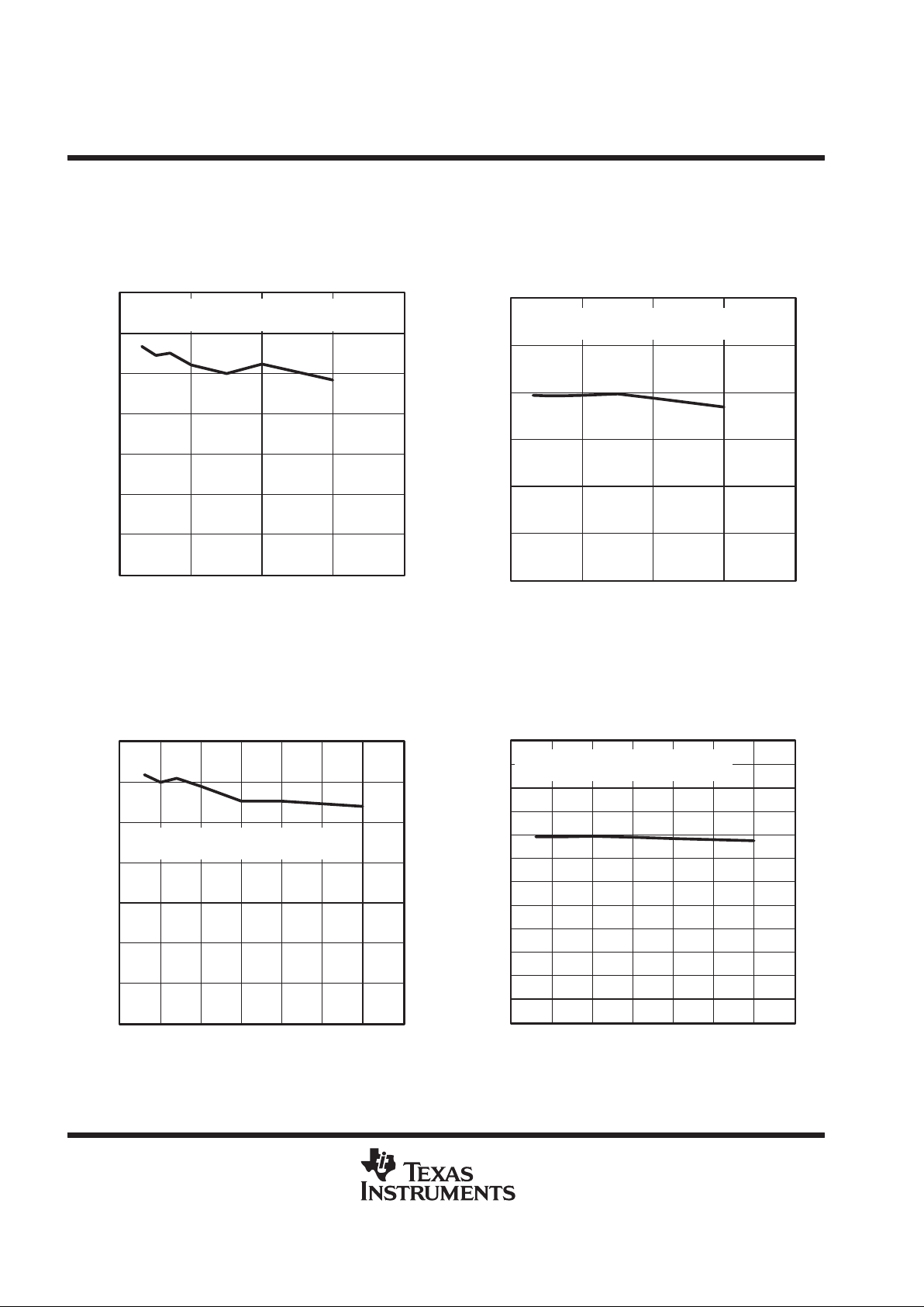
Figure 25
20
30
40
50
60
70
80
90
01234567
TOTAL HARMONIC DISTORTION
vs
SAMPLING FREQUENCY (DIFFERENTIAL)
AVDD = 5 V, DVDD = BVDD = 3 V,
fIN = 500 kHz, AIN = –0.5 dB FS
fs – Sampling Frequency – MHz
THD – Total Harmonic Distortion – dB
Figure 26
20
30
40
50
60
70
80
01234567
SIGNAL-TO-NOISE AND DISTORTION
vs
SAMPLING FREQUENCY (DIFFERENTIAL)
fs – Sampling Frequency – MHz
SINAD – Signal-to-Noise and Distortion – dB
AVDD = 5 V, DVDD = BVDD = 3 V,
fIN = 500 kHz, AIN = –0.5 dB FS
Figure 27
40
50
60
70
80
90
100
01234567
SPURIOUS FREE DYNAMIC RANGE
vs
SAMPLING FREQUENCY (DIFFERENTIAL)
fs – Sampling Frequency – MHz
SFDR – Spurious Free Dynamic Range – dB
AVDD = 5 V, DVDD = BVDD = 3 V,
fIN = 500 kHz, AIN = –0.5 dB FS
Figure 28
SIGNAL-TO-NOISE
vs
SAMPLING FREQUENCY (DIFFERENTIAL)
fs – Sampling Frequency – MHz
SNR – Signal-to-Noise – dB
20
30
40
50
60
70
80
01234567
AVDD = 5 V, DVDD = BVDD = 3 V,
fIN = 500 kHz, AIN = –0.5 dB FS
Page 34
THS10064
10-BIT 6 MSPS, SIMULTANEOUS SAMPLING
ANALOG-TO-DIGITAL CONVERTER
SLAS255 – DECEMBER 1999
34
POST OFFICE BOX 655303 • DALLAS, TEXAS 75265
TYPICAL CHARACTERISTICS
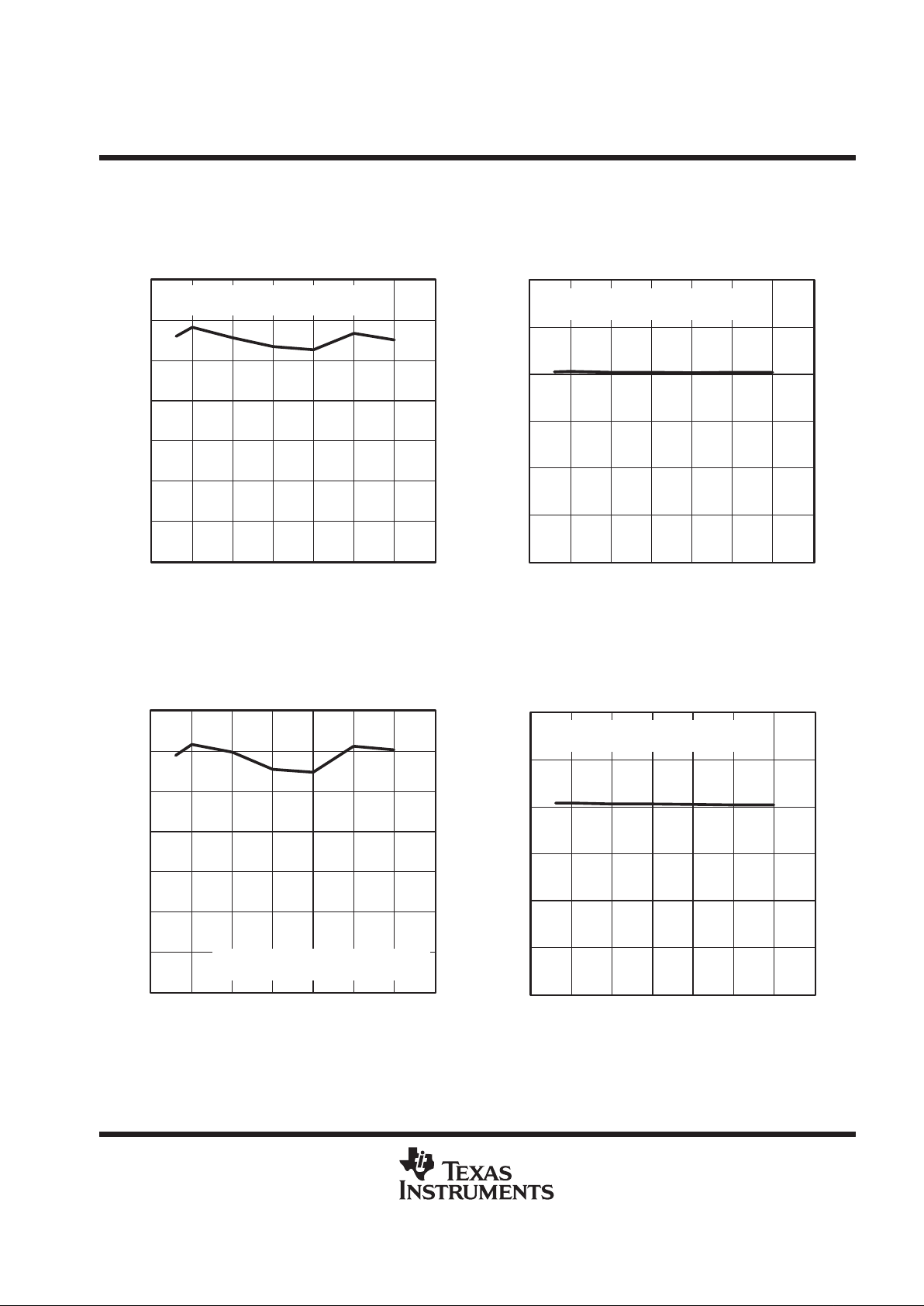
Figure 29
20
30
40
50
60
70
80
90
01234
TOTAL HARMONIC DISTORTION
vs
INPUT FREQUENCY (SINGLE-ENDED)
AVDD = 5 V, DVDD = BVDD = 3 V,
fs = 6 MSPS, AIN = –1 dB FS
fi – Input Frequency – MHz
THD – Total Harmonic Distortion – dB
Figure 30
20
30
40
50
60
70
80
01234
SIGNAL-TO-NOISE AND DISTORTION
vs
INPUT FREQUENCY (SINGLE-ENDED)
AVDD = 5 V, DVDD = BVDD = 3 V,
fs = 6 MSPS, AIN = –1 dB FS
SINAD – Signal-to-Noise and Distortion – dB
fi – Input Frequency – MHz
20
30
40
50
60
70
80
90
0 0.5 1.0 1.5 2.0 2.5 3.0 3.5
SPURIOUS FREE DYNAMIC RANGE
vs
INPUT FREQUENCY (SINGLE-ENDED)
SFDR – Spurious Free Dynamic Range – dB
fi – Input Frequency – MHz
Figure 31
AVDD = 5 V, DVDD = BVDD = 3 V,
fs = 6 MSPS, AIN = –1 dB FS
Figure 32
SIGNAL-TO-NOISE
vs
INPUT FREQUENCY (SINGLE-ENDED)
SNR – Signal-to-Noise – dB
20
25
30
35
40
45
50
55
60
65
70
75
80
0 0.5 1.0 1.5 2.0 2.5 3.0 3.5
AVDD = 5 V, DVDD = BVDD = 3 V,
fs = 6 MSPS, AIN = –1 dB FS
fi – Input Frequency – MHz
Page 35
THS10064
10-BIT 6 MSPS, SIMULTANEOUS SAMPLING
ANALOG-TO-DIGITAL CONVERTER
SLAS255 – DECEMBER 1999
35
POST OFFICE BOX 655303 • DALLAS, TEXAS 75265
TYPICAL CHARACTERISTICS
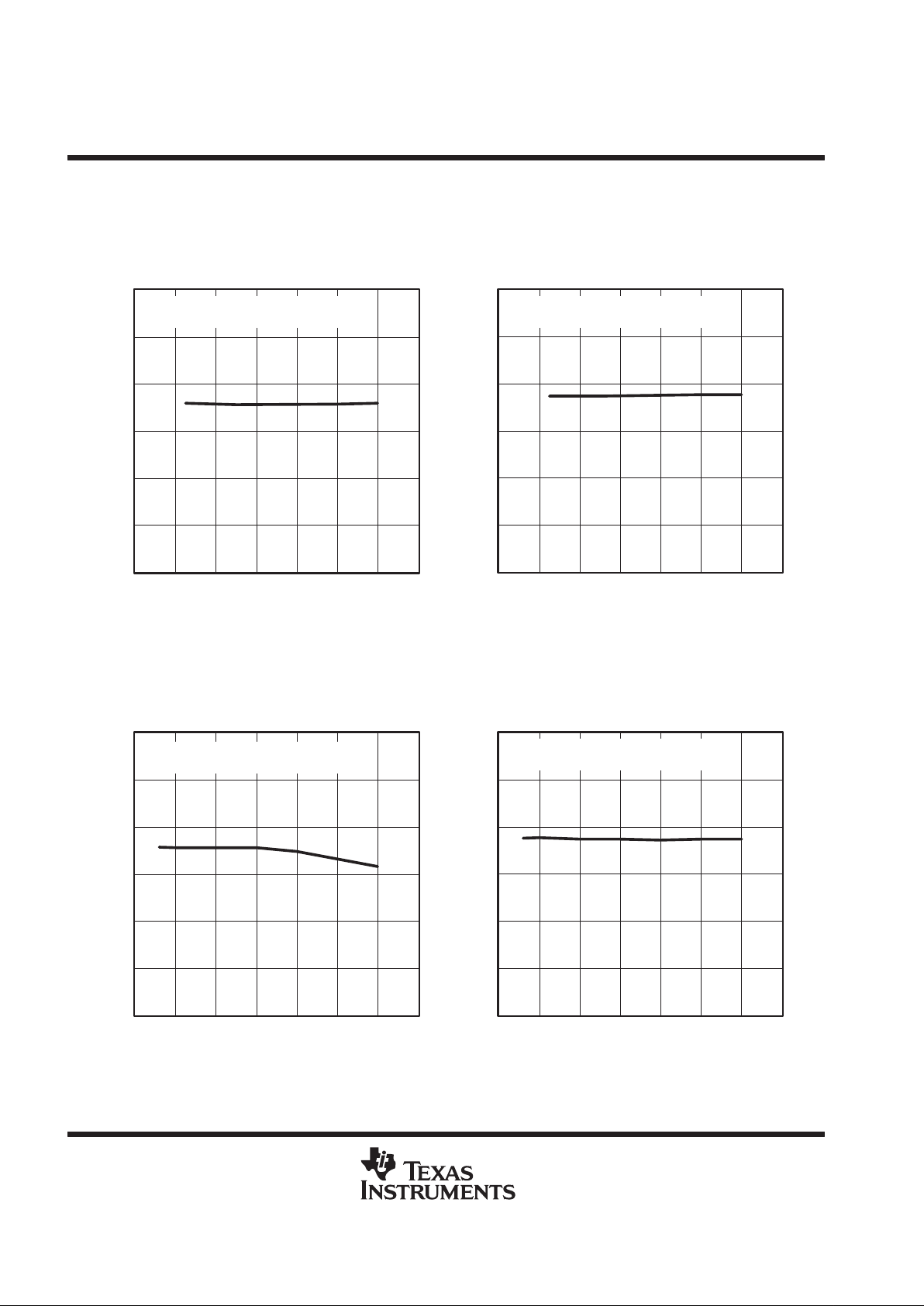
Figure 33
20
30
40
50
60
70
80
90
0 0.5 1.0 1.5 2.0 2.5 3.0 3.5
TOTAL HARMONIC DISTORTION
vs
INPUT FREQUENCY (DIFFERENTIAL)
AVDD = 5 V, DVDD = BVDD = 3 V,
fs = 6 MSPS, AIN = –0.5 dB FS
fi – Input Frequency – MHz
THD – Total Harmonic Distortion – dB
Figure 34
20
30
40
50
60
70
80
0 0.5 1.0 1.5 2.0 2.5 3.0 3.5
SIGNAL-TO-NOISE AND DISTORTION
vs
INPUT FREQUENCY (DIFFERENTIAL)
SINAD – Signal-to-Noise and Distortion – dB
AVDD = 5 V, DVDD = BVDD = 3 V,
fs = 6 MSPS, AIN = –0.5 dB FS
fi – Input Frequency – MHz
Figure 35
20
30
40
50
60
70
80
90
0 0.5 1.0 1.5 2.0 2.5 3.0 3.5
SPURIOUS FREE DYNAMIC RANGE
vs
INPUT FREQUENCY (DIFFERENTIAL)
SFDR – Spurious Free Dynamic Range – dB
AVDD = 5 V, DVDD = BVDD = 3 V,
fs = 6 MSPS, AIN = –0.5 dB FS
fi – Input Frequency – MHz
20
30
40
50
60
70
80
0 0.5 1.0 1.5 2.0 2.5 3.0 3.5
Figure 36
AVDD = 5 V, DVDD = BVDD = 3 V,
fs = 6 MSPS, AIN = –0.5 dB FS
fi – Input Frequency – MHz
SIGNAL-TO-NOISE
vs
INPUT FREQUENCY (DIFFERENTIAL)
SNR – Signal-to-Noise – dB
Page 36
THS10064
10-BIT 6 MSPS, SIMULTANEOUS SAMPLING
ANALOG-TO-DIGITAL CONVERTER
SLAS255 – DECEMBER 1999
36
POST OFFICE BOX 655303 • DALLAS, TEXAS 75265
TYPICAL CHARACTERISTICS
Figure 37
6
7
8
9
10
11
12
01234567
ENOB – Effective Number of Bits – Bits
EFFECTIVE NUMBER OF BITS
vs
SAMPLING FREQUENCY (SINGLE-ENDED)
AVDD = 5 V, DVDD = BVDD = 3 V,
fin = 500 kHz, AIN = –0.5 dB FS
fs – Sampling Frequency – MHz
Figure 38
6
7
8
9
10
11
12
01234567
ENOB – Effective Number of Bits – Bits
EFFECTIVE NUMBER OF BITS
vs
SAMPLING FREQUENCY (DIFFERENTIAL)
AVDD = 5 V, DVDD = BVDD = 3 V,
fin = 500 kHz, AIN = –0.5 dB FS
fs – Sampling Frequency – MHz
Figure 39
6
7
8
9
10
11
12
0 0.5 1.0 1.5 2.0 2.5 3.0 3.5
ENOB – Effective Number of Bits – Bits
EFFECTIVE NUMBER OF BITS
vs
INPUT FREQUENCY (SINGLE-ENDED)
AVDD = 5 V, DVDD = BVDD = 3 V,
fs = 6 MSPS, AIN = –1 dB FS
fi – Input Frequency – MHz
Figure 40
6
7
8
9
10
11
12
0 0.5 1.0 1.5 2.0 2.5 3.0 3.5
ENOB – Effective Number of Bits – Bits
EFFECTIVE NUMBER OF BITS
vs
INPUT FREQUENCY (DIFFERENTIAL)
AVDD = 5 V, DVDD = BVDD = 3 V,
fs = 6 MSPS, AIN = –0.5 dB FS
fi – Input Frequency – MHz
Page 37
THS10064
10-BIT 6 MSPS, SIMULTANEOUS SAMPLING
ANALOG-TO-DIGITAL CONVERTER
SLAS255 – DECEMBER 1999
37
POST OFFICE BOX 655303 • DALLAS, TEXAS 75265
TYPICAL CHARACTERISTICS
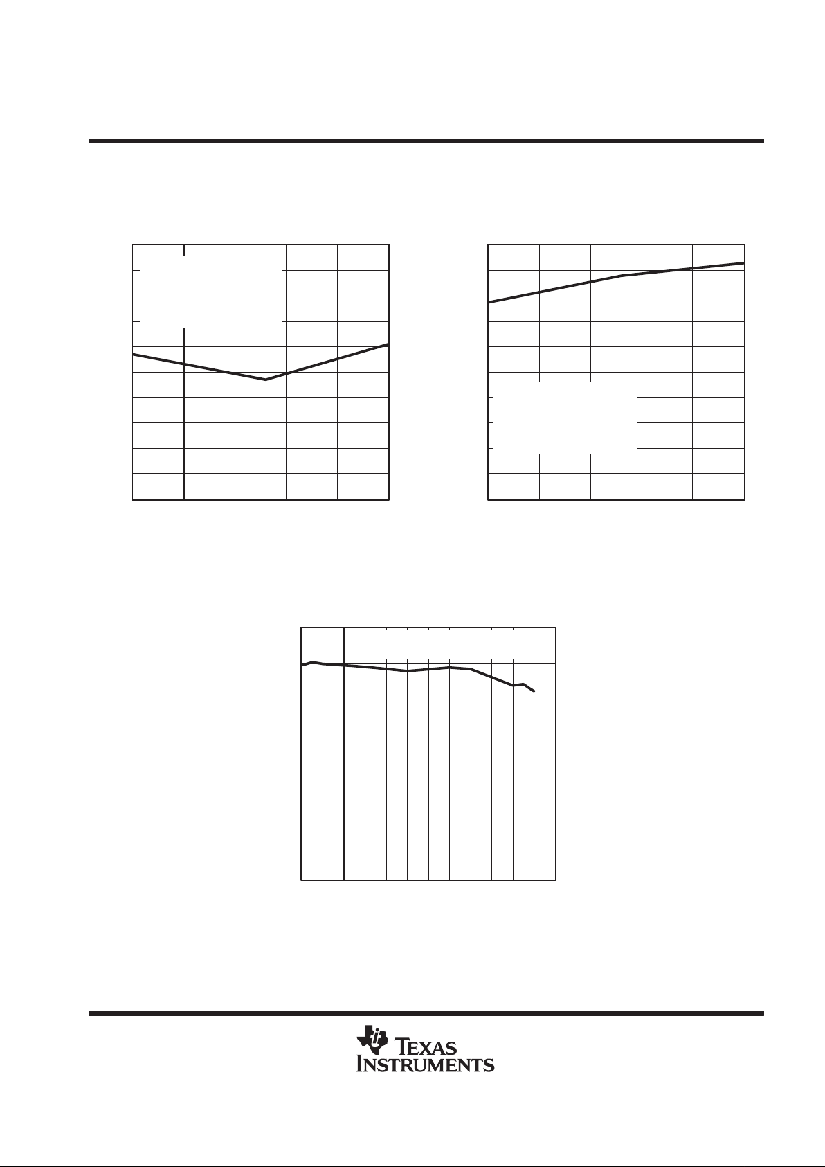
Figure 41
0.5
0.52
0.54
0.56
0.58
0.60
0.62
0.64
0.66
0.68
0.70
–40 –15 10 35 60 85
TA – Temperature – °C
INL – Integral Nonlinearity – LSB
INTEGRAL NONLINEARITY
vs
TEMPERATURE
AVDD = 5 V,
BVDD = DVDD = 3.3 V,
Differential Mode,
Internal Reference,
Internal Oscillator
Figure 42
0.5
0.52
0.54
0.56
0.58
0.60
0.62
0.64
0.66
0.68
0.70
–40 –15 10 35 60 85
TA – Temperature – °C
DNL – Differential Nonlinearity – LSB
DIFFERENTIAL NONLINEARITY
vs
TEMPERATURE
AVDD = 5 V,
BVDD = DVDD = 3.3 V,
Differential Mode,
Internal Reference,
Internal Oscillator
Figure 43
–30
–25
–20
–15
–10
–5
0
5
0 102030405060708090100110120
G – Gain – dB
GAIN
vs
INPUT FREQUENCY (SINGLE-ENDED)
AVDD = 5 V, DVDD = BVDD = 3 V,
fs = 6 MSPS, AIN = –0.5 dB FS
fi – Input Frequency – MHz
Page 38
THS10064
10-BIT 6 MSPS, SIMULTANEOUS SAMPLING
ANALOG-TO-DIGITAL CONVERTER
SLAS255 – DECEMBER 1999
38
POST OFFICE BOX 655303 • DALLAS, TEXAS 75265
TYPICAL CHARACTERISTICS
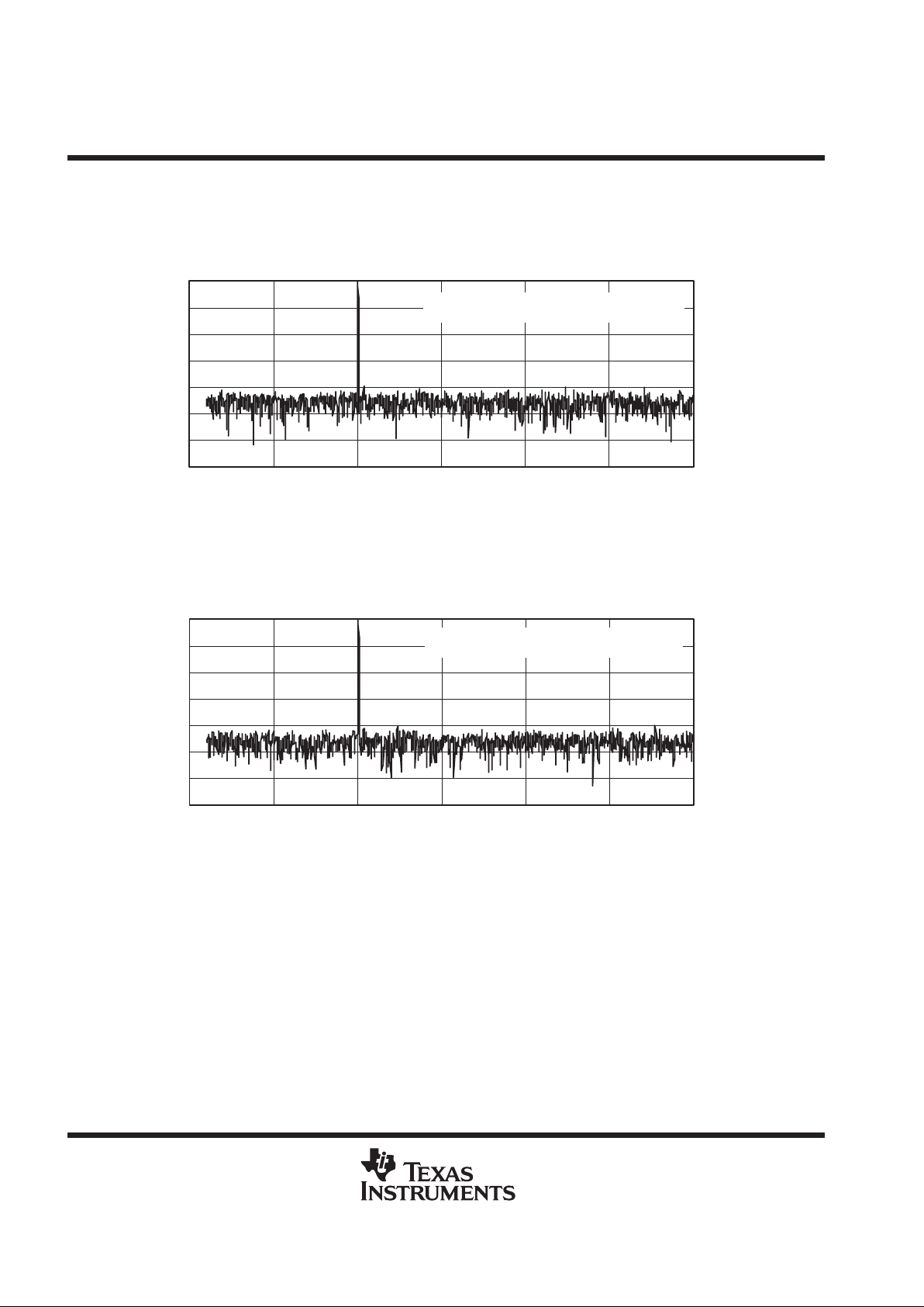
Figure 44
–140
–120
–100
–80
–60
–40
–20
0
0 0.5 1.0 1.5 2.0 2.5 3.0
Magnitude – dB
f – Frequency – MHz
FAST FOURIER TRANSFORM (4096 POINTS)
(SINGLE-ENDED)
vs
FREQUENCY
AVDD = 5 V, DVDD = BVDD = 3 V,
fs = 6 MSPS, AIN = –0.5 dB FS, fin = 1 MHz
–140
–120
–100
–80
–60
–40
–20
0
0 0.5 1.0 1.5 2.0 2.5 3.0
Figure 45
Magnitude – dB
f – Frequency – MHz
FAST FOURIER TRANSFORM (4096 POINTS)
(DIFFERENTIAL)
vs
FREQUENCY
AVDD = 5 V, DVDD = BVDD = 3 V,
fs = 6 MSPS, AIN = –0.5 dB FS, fin = 1 MHz
Page 39

THS10064
10-BIT 6 MSPS, SIMULTANEOUS SAMPLING
ANALOG-TO-DIGITAL CONVERTER
SLAS255 – DECEMBER 1999
39
POST OFFICE BOX 655303 • DALLAS, TEXAS 75265
definitions of specifications and terminology
integral nonlinearity
Integral nonlinearity refers to the deviation of each individual code from a line drawn from zero through full scale.
The point used as zero occurs 1/2 LSB before the first code transition. The full-scale point is defined as level
1/2 LSB beyond the last code transition. The deviation is measured from the center of each particular code to
the true straight line between these two points.
differential nonlinearity
An ideal ADC exhibits code transitions that are exactly 1 LSB apart. DNL is the deviation from this ideal value.
A differential nonlinearity error of less than ±1 LSB ensures no missing codes.
zero offset
The major carry transition should occur when the analog input is at zero volts. Zero error is defined as the
deviation of the actual transition from that point.
gain error
The first code transition should occur at an analog value 1/2 LSB above negative full scale. The last transition
should occur at an analog value 1 1/2 LSB below the nominal full scale. Gain error is the deviation of the actual
difference between first and last code transitions and the ideal difference between first and last code transitions.
signal-to-noise ratio + distortion (SINAD)
SINAD is the ratio of the rms value of the measured input signal to the rms sum of all other spectral components
below the Nyquist frequency, including harmonics but excluding dc. The value for SINAD is expressed in
decibels.
effective number of bits (ENOB)
For a sine wave, SINAD can be expressed in terms of the number of bits. Using the following formula,
N
+
(
SINAD*1.76
)
6.02
it is possible to get a measure of performance expressed as N, the effective number of bits. Thus, the effective
number of bits for a device for sine wave inputs at a given input frequency can be calculated directly from its
measured SINAD.
total harmonic distortion (THD)
THD is the ratio of the rms sum of the first six harmonic components to the rms value of the measured input signal
and is expressed as a percentage or in decibels.
spurious free dynamic range (SFDR)
SFDR is the difference in dB between the rms amplitude of the input signal and the peak spurious signal.
Page 40
THS10064
10-BIT 6 MSPS, SIMULTANEOUS SAMPLING
ANALOG-TO-DIGITAL CONVERTER
SLAS255 – DECEMBER 1999
40
POST OFFICE BOX 655303 • DALLAS, TEXAS 75265
MECHANICAL DATA
DA (R-PDSO-G**) PLASTIC SMALL-OUTLINE PACKAGE
38 PINS SHOWN
4040066/D 11/98
0,25
0,75
0,50
0,15 NOM
Gage Plane
6,20
NOM
8,40
7,80
32
11,10
11,10
30
Seating Plane
10,9010,90
20
0,19
19
A
0,30
38
1
PINS **
A MAX
A MIN
DIM
1,20 MAX
9,60
9,80
28
M
0,13
0°–8°
0,10
0,65
38
12,60
12,40
0,15
0,05
NOTES: A. All linear dimensions are in millimeters.
B. This drawing is subject to change without notice.
C. Body dimensions do not include mold flash or protrusion.
D. Falls within JEDEC MO-153
Page 41

IMPORTANT NOTICE
T exas Instruments and its subsidiaries (TI) reserve the right to make changes to their products or to discontinue
any product or service without notice, and advise customers to obtain the latest version of relevant information
to verify, before placing orders, that information being relied on is current and complete. All products are sold
subject to the terms and conditions of sale supplied at the time of order acknowledgement, including those
pertaining to warranty, patent infringement, and limitation of liability.
TI warrants performance of its semiconductor products to the specifications applicable at the time of sale in
accordance with TI’s standard warranty. Testing and other quality control techniques are utilized to the extent
TI deems necessary to support this warranty. Specific testing of all parameters of each device is not necessarily
performed, except those mandated by government requirements.
CERT AIN APPLICATIONS USING SEMICONDUCTOR PRODUCTS MAY INVOLVE POTENTIAL RISKS OF
DEATH, PERSONAL INJURY, OR SEVERE PROPERTY OR ENVIRONMENTAL DAMAGE (“CRITICAL
APPLICATIONS”). TI SEMICONDUCTOR PRODUCTS ARE NOT DESIGNED, AUTHORIZED, OR
WARRANTED TO BE SUITABLE FOR USE IN LIFE-SUPPORT DEVICES OR SYSTEMS OR OTHER
CRITICAL APPLICATIONS. INCLUSION OF TI PRODUCTS IN SUCH APPLICA TIONS IS UNDERSTOOD T O
BE FULLY AT THE CUSTOMER’S RISK.
In order to minimize risks associated with the customer’s applications, adequate design and operating
safeguards must be provided by the customer to minimize inherent or procedural hazards.
TI assumes no liability for applications assistance or customer product design. TI does not warrant or represent
that any license, either express or implied, is granted under any patent right, copyright, mask work right, or other
intellectual property right of TI covering or relating to any combination, machine, or process in which such
semiconductor products or services might be or are used. TI’s publication of information regarding any third
party’s products or services does not constitute TI’s approval, warranty or endorsement thereof.
Copyright 1999, Texas Instruments Incorporated
 Loading...