

Page 1
HIGH VOLTAGE FAST-SWITCHING
■ STMicroelectronics PREFERRED
SALESTYPE
■ HIGH VOLTAGECAPABILITY
■ U.L.RECOGNISED ISOWATT218PACKAGE
(U.L. FILE # E81734(N))
■ NPNTRANSISTOR WITH INTEGRATED
FREEWHEELINGDIODE.
THD218DHI
NPN POWER TRANSISTOR
APPLICATIONS
■ HORIZONTAL DEFLECTIONFOR COLOUR
TV
DESCRIPTION
This devices is manufacturedusingMultiepitaxial
Mesa technology for cost-effective high
performance and uses a Hollow Emitter structure
to enhanceswitchingspeeds.
The THDseries is designed for use in horizontal
deflectioncircuits in televisionsand monitors.
ABSOLUTE MAXIMUM RATINGS
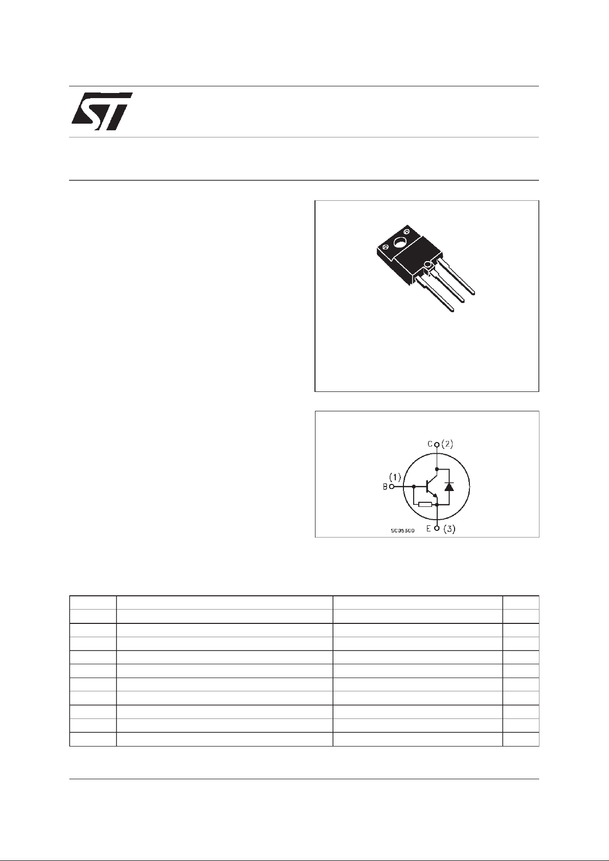
3
2
1
ISOWATT218
INTERNAL SCHEMATIC DIAGRAM
Symb o l Parame t er Val u e Uni t
V
V
V
I
I
P
T
December 1999
Collector-Base Voltage (IE= 0) 1500 V
CBO
Collector-Emitter V oltage (IB= 0) 700 V
CEO
Emitter-Base Voltage (IC=0) 10 V
EBO
Collect or Current 7 A
I
C
Collect or Peak Cu rr ent (tp<5ms) 12 A
CM
Base Current 4 A
I
B
Base Peak Cu r rent (tp<5ms) 7 A
BM
Total Dis sipati on at Tc=25oC50W
tot
Stora ge Temperat u re -65 t o 150
stg
Max. O perat i ng J unc t i on Temperat u r e 150
T
j
o
C
o
C
1/6
Page 2
THD218DHI
THERMAL DATA
R
thj-case
Ther mal Resistance Junct ion-case Max 2.5
o
C/W
ELECTRICAL CHARACTERISTICS (T
=25oC unless otherwise specified)
case
Symbol Parameter Test Cond itions Min. Typ. Max. Un it
I
I
V
CE(sat)
CES
Collector Cut- of f
Current (V
EBO
Emit ter Cut -off Current
=0)
(I
C
∗ Collector-E mitt er
BE
=0)
V
=1500V
CE
=1500V Tj= 125oC
V
CE
V
=5V 300 mA
EB
0.2
2
IC=4A IB=1A 1.5 V
Saturation Voltage
V
BE(sat )
∗ Base-Emitt er
IC=4A IB=1A 1.3 V
Saturation Voltage
∗ DC Current Gain IC=4A VCE=5V
h
FE
INDUCTI VE LO AD
t
V
∗
Pulsed: Pulse duration = 300 µs, duty cycle 1.5 %
St orage Time
s
t
Fall Time
f
Diode Forward Voltage IF=4A 2.5 V
F
=4A VCE=5V Tj= 100oC
I
C
IC= 4 A f = 15625 Hz
=1A IB2=-2A
I
B1
V
ceflyback
= 1050 sin
5
3.5
4.7
π
6
tV
10
5
0.48
10
mA
mA
µs
µs
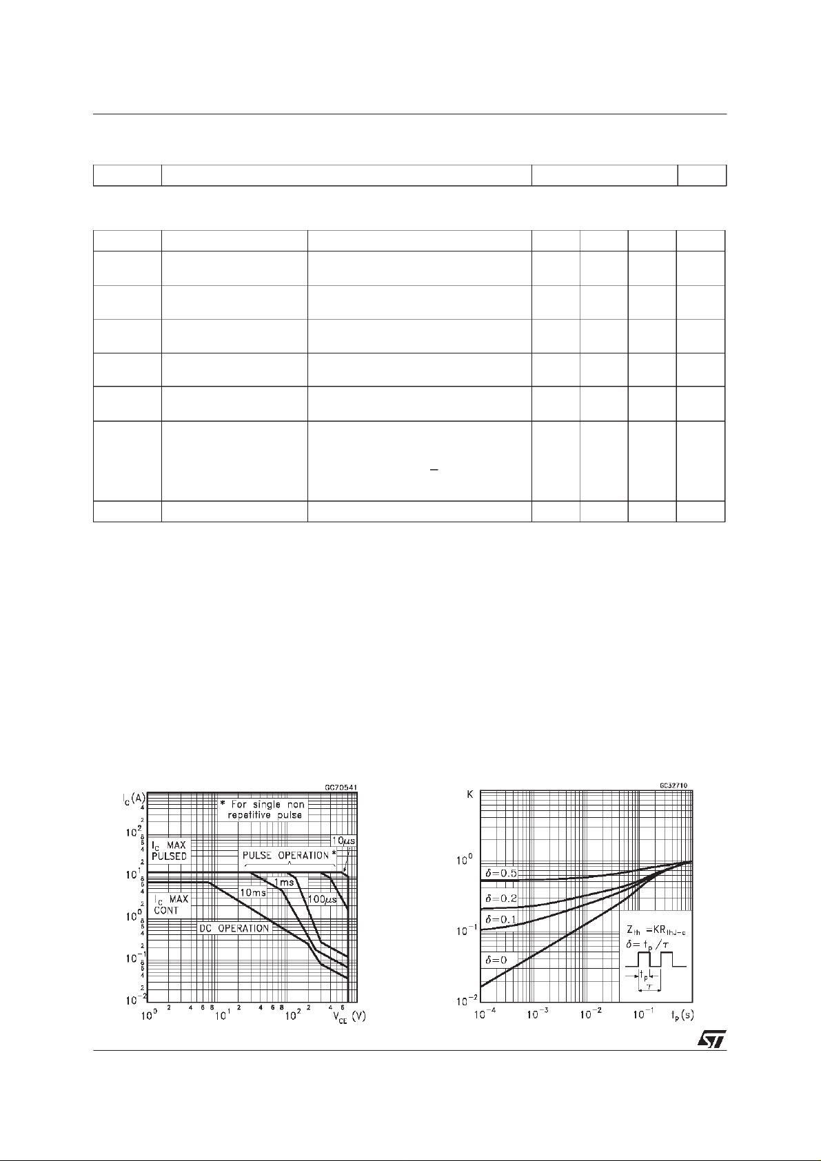
Safe OperatingArea ThermalImpedance
2/6
Page 3

THD218DHI
Derating Curve
CollectorEmitter SaturationVoltage
DC Current Gain
BaseEmitter Saturation Voltage
InductiveFall TimeI
InductiveStorage Time
3/6
Page 4

THD218DHI
ReverseBiased SOA
BASEDRIVE INFORMATION
In order to saturate the power switch and reduce
conduction losses, adequate direct base current
I
has to be provided for the lowest gain hFEat
B1
o
C (line scan phase). On the other hand,
100
negative base current I
turn off the powertransistor (retracephase).
Most of the dissipation, in the deflection
application, occurs at switch-off. Therefore it is
essential to determine the value of I
minimizes power losses, fall time t
consequently,T
. A new set of curves have been
j
defined to give total power losses, t
function of I
at both 16 KHz and 32 KHz
B2
scanning frequencies for choosing the optimum
negative drive. The test circuit is illustrated in
must be provided to
B2
B2
and tfas a
s
which
f
and,
figure 1.
Inductance L
negative base current I
serves to control the slope of the
1
to recombine the
B2
excess carrier in the collector when base current
is still present, this would avoid any tailing
phenomenonin the collectorcurrent.
The values of L and C are calculated from the
followingequations:
C
)2=
1
2
C(V
CEfly
2
)
ω=2π
1
f
=
√
L
C
CEfly
1
L(I
2
Where IC= operating collector current, V
flyback voltage, f= frequency of oscillation during
retrace.
=
Figure 1: Inductive Load Switching Test Circuit.
4/6
Page 5

ISOWATT218MECHANICAL DATA
THD218DHI
DIM.
A 5.35 5.65 0.211 0.222
C 3.30 3.80 0.130 0.150
D 2.90 3.10 0.114 0.122
D1 1.88 2.08 0.074 0.082
E 0.75 0.95 0.030 0.037
F 1.05 1.25 0.041 0.049
F2 1.50 1.70 0.059 0.067
F3 1.90 2.10 0.075 0.083
G 10.80 11.20 0.425 0.441
H 15.80 16.20 0.622 0.638
L 9 0.354
L1 20.80 21.20 0.819 0.835
L2 19.10 19.90 0.752 0.783
L3 22.80 23.60 0.898 0.929
L4 40.50 42.50 1.594 1.673
L5 4.85 5.25 0.191 0.207
L6 20.25 20.75 0.797 0.817
N 2.1 2.3 0.083 0.091
R 4.6 0.181
DIA 3.5 3.7 0.138 0.146
MIN. TYP. MAX. MIN. TYP. MAX.
mm inch
- Weight : 4.9g (typ.)
- Maximum Torque (applied to mountingflange) Recommended: 0.8 Nm; Maximum:1 Nm
- The side of thedissipator must beflat within 80 µm
P025C/A
5/6
Page 6

THD218DHI
Information furnished is believed to be accurate and reliable. However, STMicroelectronics assumes no responsibility for the consequences
of use of such information nor for any infringement of patents or other rights of third parties which may result from its use. No license is
granted by implication or otherwise under any patent or patent rights of STMicroelectronics. Specification mentioned in this publication are
subject tochange without notice. This publication supersedes and replaces all information previously supplied. STMicroelectronics products
are not authorized for use as critical components in life support devices or systems without express written approval of STMicroelectronics.
The ST logo is a trademark of STMicroelectronics
1999 STMicroelectronics – Printed in Italy – All Rights Reserved
STMicroelectronicsGROUP OF COMPANIES
Australia - Brazil - China - Finland - France - Germany - Hong Kong - India - Italy- Japan - Malaysia - Malta - Morocco -
Singapore- Spain - Sweden - Switzerland - United Kingdom - U.S.A.
http://www.st.com
.
6/6
 Loading...