

Page 1
HIGH VOLTAGE FAST-SWITCHING
■ STMicroelectronics PREFERRED
SALESTYPE
■ HIGH VOLTAGECAPABILITY
■ VERYHIGH SWITCHING SPEED
■ U.L.RECOGNISED ISOWATT218PACKAGE
(U.L. FILE # E81734(N))
THD200FI
NPN POWER TRANSISTOR
APPLICATIONS:
■ HORIZONTAL DEFLECTIONFOR
MONITORS
DESCRIPTION
The THD200FI is manufactured using
Multiepitaxial Mesa technology for cost-effective
high performance and uses a Hollow Emitter
structureto enhance switching speeds.
The THDseries is designed for use in horizontal
deflectioncircuits in televisionsand monitors.
ABSOLUTE MAXIMUM RATINGS
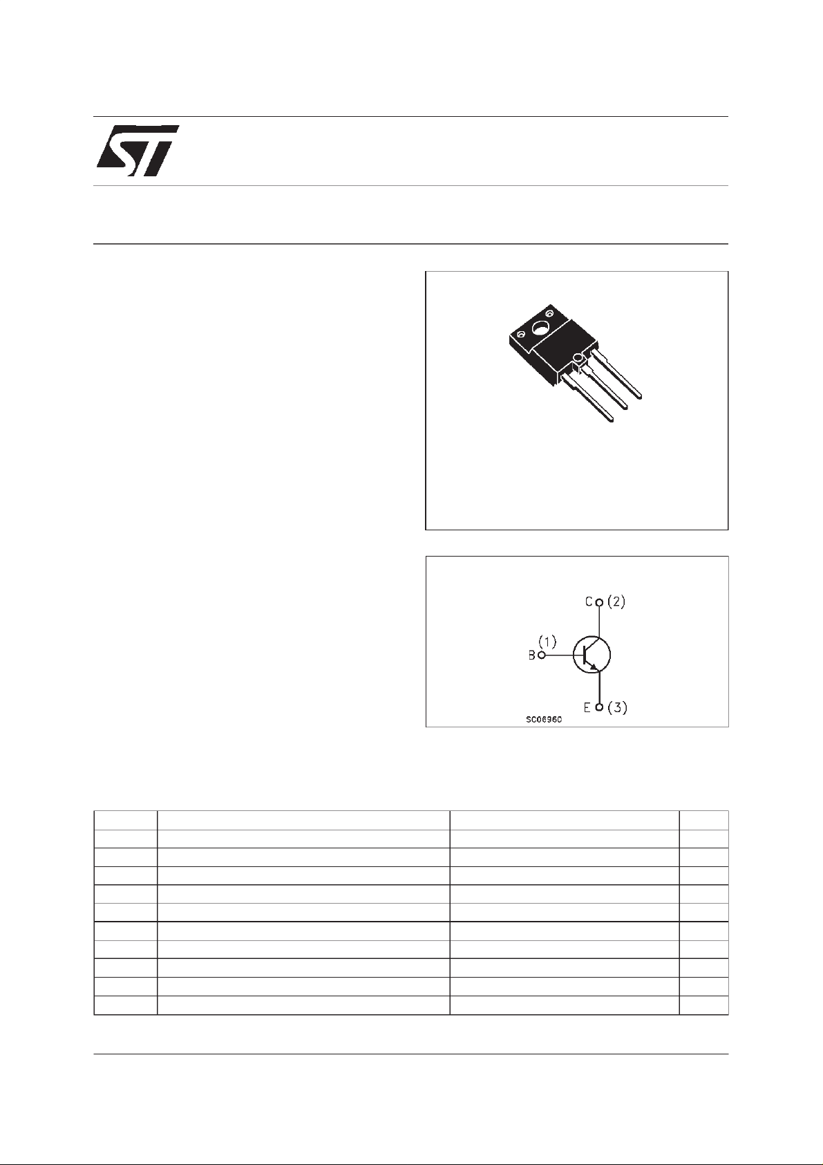
3
2
1
ISOWATT218
INTERNAL SCHEMATIC DIAGRAM
Symb o l Parame t er Val u e Uni t
V
V
V
I
I
P
T
December 1999
Collector-Base Voltage (IE= 0) 1500 V
CBO
Collector-Emitter V oltage (IB= 0) 700 V
CEO
Emitter-Base Voltage (IC=0) 10 V
EBO
Collect or Current 10 A
I
C
Collect or Peak Cu rr ent ( tp<5ms) 20 A
CM
Base Current 5 A
I
B
Base Peak Cu r rent (tp<5ms) 10 A
BM
Total Dis sipation at Tc=25oC57W
tot
Stora ge Temper at u re -65 t o 150
stg
Max. O perating Junct i on T em per at u r e 150
T
j
o
C
o
C
1/7
Page 2

THD200FI
THERMAL DATA
R
thj-case
Ther mal Resistance Junc t io n- case Max 2.2
o
C/W
ELECTRICAL CHARACTERISTICS (T
=25oC unless otherwisespecified)
case
Symbol Parameter Test Cond itions Min. Typ. Max. Unit
I
CES
I
EBO
V
CEO(sus )
Collector Cut -off
Current (V
BE
=0)
Emit ter Cut- o f f Curr ent
=0)
(I
C
∗ Co llector-Emit t er
V
=1500V
CE
=1500V Tj= 125oC
V
CE
V
=5V 100 µA
EB
I
= 100 mA 700 V
C
0.2
2
Sust aining Voltage
=0)
(I
C
V
V
CE(sat)
EBO
Emitt er-Base Voltage
=0)
(I
B
∗ Collector- E mitter
I
=10mA 10 V
E
IC=7A IB= 1.5 A 1.5 V
Saturation Voltage
V
BE(sat)
∗ Base-Emitt er
IC=7A IB= 1.5 A 1.3 V
Saturation Voltage
∗ DC Cur rent Gain IC=7A VCE=5V
h
FE
t
t
RESI STIVE LO AD
St orage Time
s
t
Fall Time
f
INDUCTIVE LO A D
St orage Time
s
t
Fall Time
f
=7A VCE=5V Tj=100oC
I
C
VCC=400V IC=7A
=1.5A IB2= 3.5 A 2.1
I
B1
IC= 7 A f = 31250 Hz
=1.5A IB2=-3.5A
I
B1
V
ceflyback
= 1200 sin
6.5
4
140
3.5
π
6
tV
10
5
320
13
3.1
210
mA
mA
µs
ns
µs
ns
INDUCTIVE LO A D
t
∗
Pulsed: Pulse duration = 300 µs, duty cycle 1.5 %
s
t
f
St orage Time
Fall Time
2/7
IC=7A f=64KHz
=1.5A IB2=-3.5A
I
B1
π
V
ceflyback
= 1200 sin
10
5
6
tV
1.7
215
µs
ns
Page 3
THD200FI
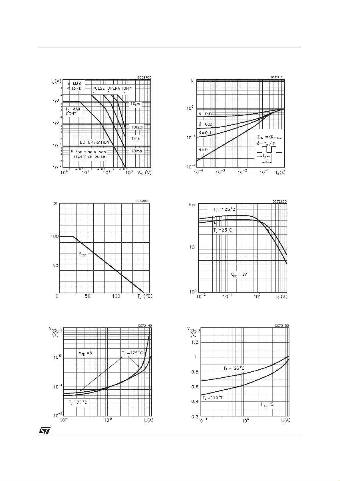
Safe OperatingArea
Derating Curve
Thermal Impedance
DC Current Gain
CollectorEmitter SaturationVoltage
BaseEmitter Saturation Voltage
3/7
Page 4

THD200FI
PowerLosses at 32 KHz
PowerLosses at 64 KHz
Switching Time InductiveLoad at 32KHz
(see figure2)
SwitchingTime Inductive Loadat 64 KHz
(see figure2)
ReverseBiased SOA
4/7
Page 5

BASEDRIVE INFORMATION
THD200FI
In order to saturate the power switch and reduce
conduction losses, adequate direct base current
I
hasto be providedfor the lowestgain hFEat T
B1
= 100oC (line scan phase). On the other hand,
negative base current I
must be provided turn
B2
off the power transistor (retrace phase). Most of
the dissipation, especially in the deflection
application, occurs at switch-off so it is essential
to determine the value of I
power losses, fall time t
and, consequently, Tj.A
f
which minimizes
B2
new set of curves have been defined to give total
power losses, t
and tfasa function of IB2at both
s
32 KHz and 64 KHz scanning frequencies in
order to choice the optimum negative drive. The
testcircuit is illustratedin fig. 1.
Figure 1: Inductive Load Switching Test Circuit.
Inductance L
negative base current I
the excess carriers in the collector when base
j
serves to control the slope of the
1
in order to recombine
B2
current is still present, thus avoiding any tailing
phenomenonin the collectorcurrent.
The values of L and C are calculated from the
followingequations:
1
L(I
2
ω=2πf=
C
)2=
1
2
1
√
L
C(V
C
CEfly
2
)
Where IC= operating collector current, V
flyback voltage, f= frequency of oscillation during
retrace.
CEfly
=
Figure2: SwitchingWaveformsin a DeflectionCircuit.
5/7
Page 6

THD200FI
ISOWATT218MECHANICAL DATA
DIM.
A 5.35 5.65 0.211 0.222
C 3.30 3.80 0.130 0.150
D 2.90 3.10 0.114 0.122
D1 1.88 2.08 0.074 0.082
E 0.75 0.95 0.030 0.037
F 1.05 1.25 0.041 0.049
F2 1.50 1.70 0.059 0.067
F3 1.90 2.10 0.075 0.083
G 10.80 11.20 0.425 0.441
H 15.80 16.20 0.622 0.638
L 9 0.354
L1 20.80 21.20 0.819 0.835
L2 19.10 19.90 0.752 0.783
L3 22.80 23.60 0.898 0.929
L4 40.50 42.50 1.594 1.673
L5 4.85 5.25 0.191 0.207
L6 20.25 20.75 0.797 0.817
N 2.1 2.3 0.083 0.091
R 4.6 0.181
DIA 3.5 3.7 0.138 0.146
MIN. TYP. MAX. MIN. TYP. MAX.
mm inch
- Weight : 4.9 g (typ.)
- Maximum Torque (applied to mountingflange) Recommended: 0.8 Nm; Maximum:1 Nm
- The side of thedissipator must beflat within 80 µm
6/7
P025C/A
Page 7

THD200FI
Information furnished is believed to be accurate and reliable. However, STMicroelectronics assumes no responsibility for theconsequences
of use of such information nor for any infringement of patents or other rights of third parties which may result from its use. No license is
granted by implication or otherwise under anypatent or patent rights of STMicroelectronics. Specification mentioned in this publication are
subject to change without notice. This publication supersedes and replaces all information previously supplied. STMicroelectronics products
are not authorized for useas critical components in life support devices orsystems without express written approval of STMicroelectronics.
Australia - Brazil - China - Finland - France- Germany - Hong Kong - India - Italy - Japan - Malaysia - Malta - Morocco -
The ST logo is a trademarkof STMicroelectronics
1999 STMicroelectronics – Printed in Italy – All Rights Reserved
STMicroelectronicsGROUP OF COMPANIES
Singapore- Spain - Sweden - Switzerland - United Kingdom - U.S.A.
http://www.st.com
.
7/7
 Loading...