

Page 1

TH71111
868/915MHz
FSK/FM/ASK Receiver
Features
! Single superhet architecture for low external component count
! FSK for digital data and FM reception for analog signal transmission
! FM/FSK demodulation with phase-coincidence demodulator
! Low current consumption in active mode and very low standby current
! Switchable LNA gain for improved dynamic range
! RSSI allows signal strength indication and ASK detection
! Surface mount package LQFP32
Ordering Information
Part No. Temperature Range Package
TH71111 -40 °C to 85°C LQFP32
Application Examples
! General digital and analog 868 MHz or 915 MHz ISM band usage
! Low-power telemetry
! Alarm and security systems
! Keyless car and central locking
! Pagers
Technical Data Overview
! Input frequency range: 800 MHz to 930 MHz
! Power supply range: 2.5 V to 5.5 V at 868 MHz and 3.3 V to 5.5 V at 915 MHz
! Temperature range: -40 °C to +85 °C
! Operating current: 7.5 mA at low gain and 9.2 mA at high gain mode
! Standby current: < 100 nA
! Sensitivity: -109 dBm
! Sensitivity: -102 dBm
! Range of IF: 455 kHz to 21.4 MHz
! Maximum input level: –10 dBm at ASK and 0 dBm at FSK
! Image rejection: > 55 dB (e.g. with SAW front-end filter and at 10.7 MHz IF)
! Spurious emission: < -70 dBm
! Input frequency acceptance: ±50 kHz (with AFC option)
! RSSI range: 70 dB
! Frequency deviation range: ±5 kHz to ±120 kHz
! Maximum data rate: 80 kbit/s NRZ
! Maximum analog modulation frequency: 15 kHz
1)
at ± 8 kHz FSK deviation, BER = 3⋅10-3 and phase-coincidence demodulation
2)
at ± 50 kHz FSK deviation, BER = 3⋅10-3 and phase-coincidence demodulation
1)
with 40 kHz IF filter BW (incl. SAW front-end filter loss)
2)
with 150 kHz IF filter BW (incl. SAW front-end filter loss)
TH71111 Data Sheet Page 1 of 20 Nov. 2001
3901071111 Rev. 005
Page 2
TH71111
868/915MHz
FSK/FM/ASK Receiver
General Description
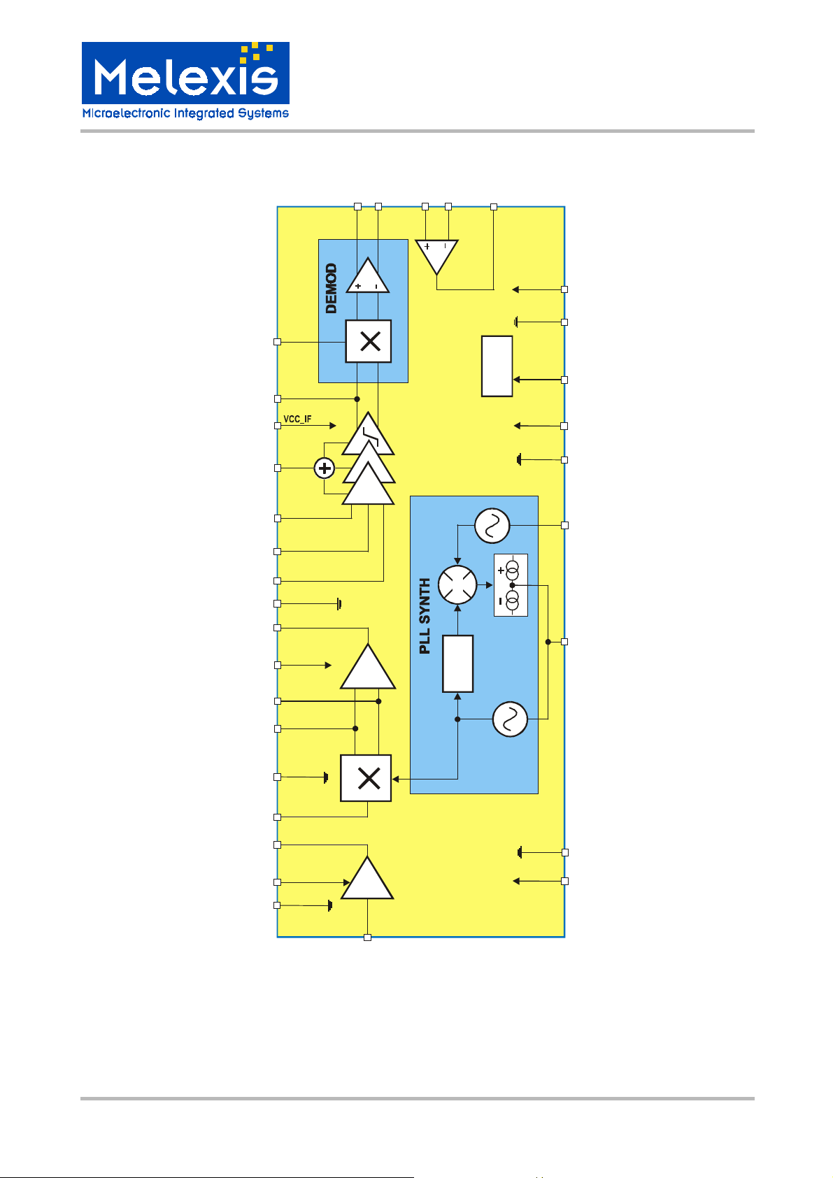
The TH71111 receiver IC consists of the following building blocks
" PLL synthesizer (PLL SYNTH) for generation of the local oscillator signal LO
" Parts of the PLL SYNTH are the high-frequency VCO1, the feedback divider DIV_32,
a phase-frequency detector (PFD) with charge pump (CP) and a crystal-based reference oscillator (RO)
" Low-noise amplifier (LNA) for high-sensitivity RF signal reception
" First mixer (MIX1) for down-conversion of the RF signal to the IF
" IF pre amplifier which is a mixer cell (MIX2) that operates as an amplifier
" IF amplifier (IFA) to amplify and limit the IF signal and for RSSI generation
" Phase coincidence demodulator (DEMOD) with third mixer (MIX3) to demodulate the IF signal
" Operational amplifier (OA) for data slicing, filtering and ASK detection
" Bias circuitry for bandgap biasing and circuit shutdown
With the T H71111 receiver c hip, various circuit c onfigurations c an be arranged in or der to m eet a num ber of
different custom er requirements . For FM/FSK reception the IF tank used in the phase coincidence dem odulator can be constituted either by a ceramic resonator or an LC tank (optionally with a varactor diode to create
an AFC circuit). In ASK configuration, the RSSI signal is feed to an ASK detector, which is constituted by the
operational amplifier.
Demodulation Type of receiver
FM / FSK
FM / FSK
ASK
A double-conversion variant, called TH71112, is also available. This receiver IC allows a higher degree of
image rejection, achieved in conj unction with an RF frontend filter. Both RXICs have the sam e die. At the
TH71112, the second mixer (MIX2) is used to down-convert the first IF (IF1) to the second IF (IF2). At the
TH71111, MIX2 operates as an amplifier.
Efficient RF frontend f iltering is realized by using a SAW, ceramic or helix filter in front of the LNA and by
adding an LC filter at the LNA output.
narrow-band RX with ceramic demodulation tank
wide-band RX with LC demodulation tank
RX with RSSI-based demodulation
TH71111 Data Sheet Page 2 of 20 Nov. 2001
3901071111 Rev. 005
Page 3
Block Diagram
TH71111
868/915MHz
FSK/FM/ASK Receiver
IN_DEM
OUT_IFA
14
RSSI
21
FPC2
13 15 16
FBC1
12
IN_IFA
11
VEE_IF
10
OUT_MIX2
93
VCC_MIX
8
IF1N
7
IF1P
6
24
23
OUTP
OUTN
20
19
OAP
OAN
18
OUT_OA
OA
VCC_BIAS
17
VEE_BIAS
22
MIX3
ENRX
BIAS
28
VCC_PLL
27
VEE_RO
25
IFA
RO
RO
26
PFD
IF
CP
MIX2
IF
DIV_32
LF
29
VEE_MIX
5
IN_MIX1
4
OUT_LNA
GAIN_LNA
2
VEE_LNAC
1
LO
MIX1
LNA
IN_LNA
31
VCO1
VEE_LNA
30
VCC_LNA
32
Fig. 1: TH71111 block diagram
TH71111 Data Sheet Page 3 of 20 Nov. 2001
3901071111 Rev. 005
Page 4
TH71111
868/915MHz
FSK/FM/ASK Receiver
Frequency Planning
Frequency planning is straightforward for single-conversion applications because there is only one IF that
might be chosen, and then the only possible choice is low-side or high-side inj ection of the LO signal (which
is now the one and only LO signal in the receiver).
The receiver’s single-conversion architecture requires careful frequency planning. Besides the desired RF
input signal, there are a number of s purious signals that may cause an undesired response at the output.
Among them is the image of the RF signal that must be suppressed by the RF front-end filter.
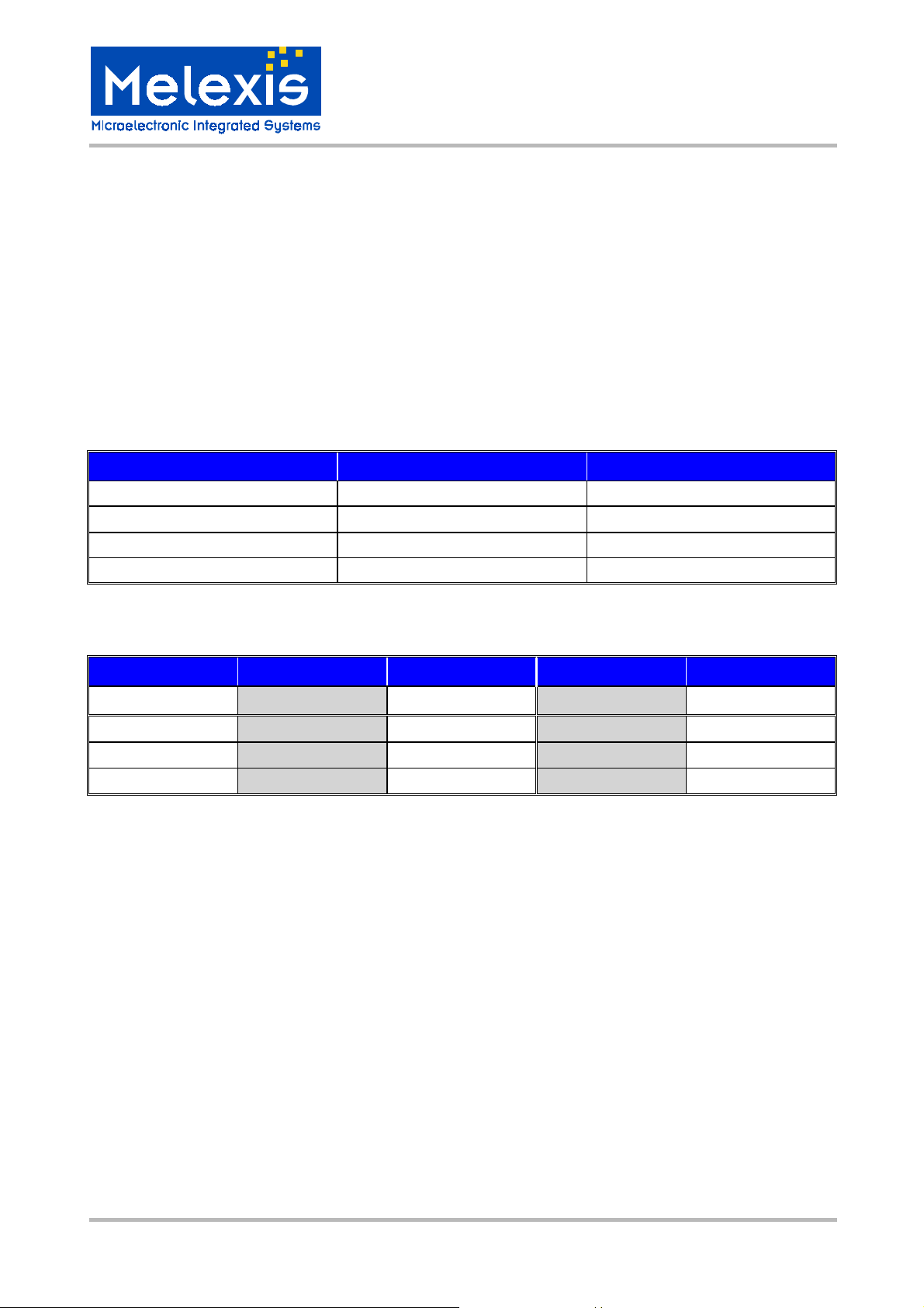
By using the internal PLL synthesizer of the TH71111 with the fixed feedback divider ratio of N = 32 (DIV_32),
two types of down-conversion are possible: low-side injection of LO and high-side injection of LO . The following table summarizes some equations that are useful to calc ulate the crystal reference frequency (REF),
the IF and the LO frequency respectively, for a given RF.
Injection type low high
REF (RF – IF)/32 (RF + IF)/32
LO
IF RF – LO LO – RF
RF image RF – 2IF RF + 2IF
32•REF 32•REF
The following table depicts crystal, LO and image signals considering the examples of 868.3 MHz and
915 MHz RF reception at IF = 10.7 MHz.
Signal type RF = 868.3 MHz RF = 868.3 MHz RF = 915 MHz RF = 915 MHz
Injection type
REF / MHz
LO / MHz
RF image / MHz
The selection of the reference crystal frequency is based on some as sumptions. As for example: the image
frequency should not be in a radio band where strong interfering signals might occur (bec ause they could
represent parasitic receiving s ignals), the LO s ignal should be in the range of 800 MHz to 915 MHz (because
this is the optimum frequency range of the VCO1). Furthermore the IF should be as high as possible to
achieve highest RF image rejec tion. The columns in bold depict the selected frequency plans to rec eive at
866.3 MHz and 915 MHz, respectively.
Low
26.80000
857.6
846.9
high
27.46875
879.0
889.7
low
28.25938
904.3
893.6
high
28.92813
925.7
936.4
TH71111 Data Sheet Page 4 of 20 Nov. 2001
3901071111 Rev. 005
Page 5
TH71111
868/915MHz
FSK/FM/ASK Receiver
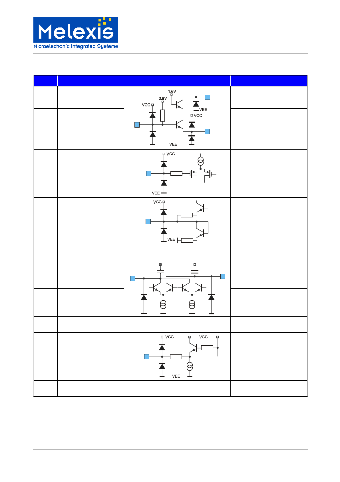
Pin Definition and Descripti on
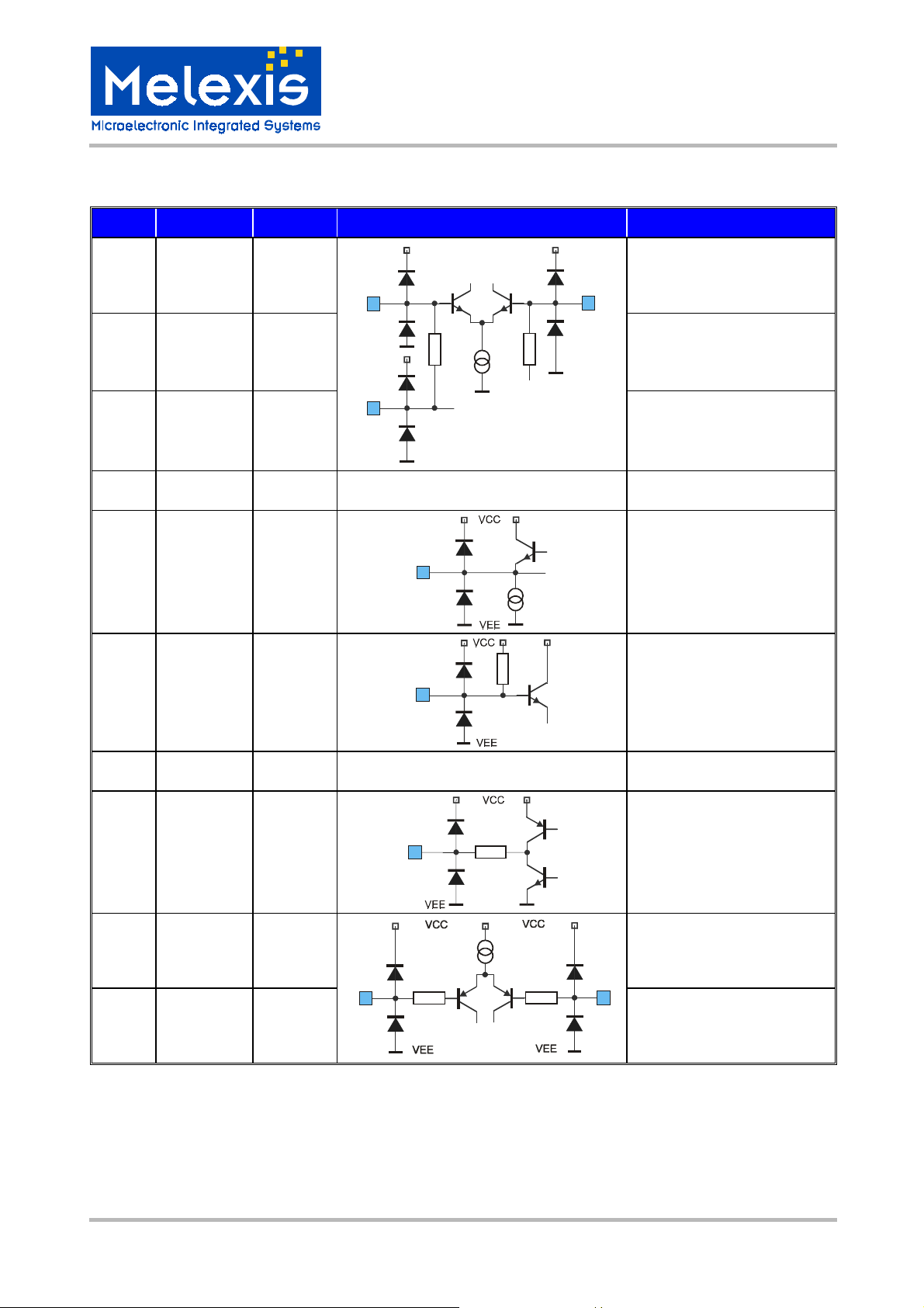
Pin No. Name I/O Type Functional Schematic Description
3 OUT_LNA analog
output
31 IN_LNA analog
input
1 VEE_LNAC ground
2 GAIN_LNA analog
input
IN_LNA
31
GAIN_LNA
2
5k
400
Ω
OUT_LNA
3
VEE_LNAC
1
LNA open-collector output,
to be connected to external
LC tank that resonates at RF
LNA input, approx.
26Ω single-ended
ground of LNA core
(cascode)
LNA gain control (CMOS
input with hysteresis)
4 IN_MIX1 analog
input
IN_MIX1
4
Ω
13
Ω
13
500µA
MIX1 input, approx. 33Ω
single-ended
5 VEE_MIX ground LNA biasing ground
6 IF1P analog I/O open-collector output, to be
IF1P
6
7 IF1N analog I/O
VEE
VCC
20p
2x500µA
20p
VEE
IF1N
connected to external LC
tank that resonates at first IF
7
open-collector output, to be
connected to external LC
tank that resonates at first IF
8 VCC_MIX supply MIX1 and MIX2 positive
supply
9 OUT_MIX2 analog
output
OUT_MIX2
9
130
6.8k
Ω
230µA
MIX2 output, approx. 330Ω
output impedance
10 VEE_IF ground ground for MIX2, IFA and
DEMOD
TH71111 Data Sheet Page 5 of 20 Nov. 2001
3901071111 Rev. 005
Page 6
TH71111
868/915MHz
FSK/FM/ASK Receiver
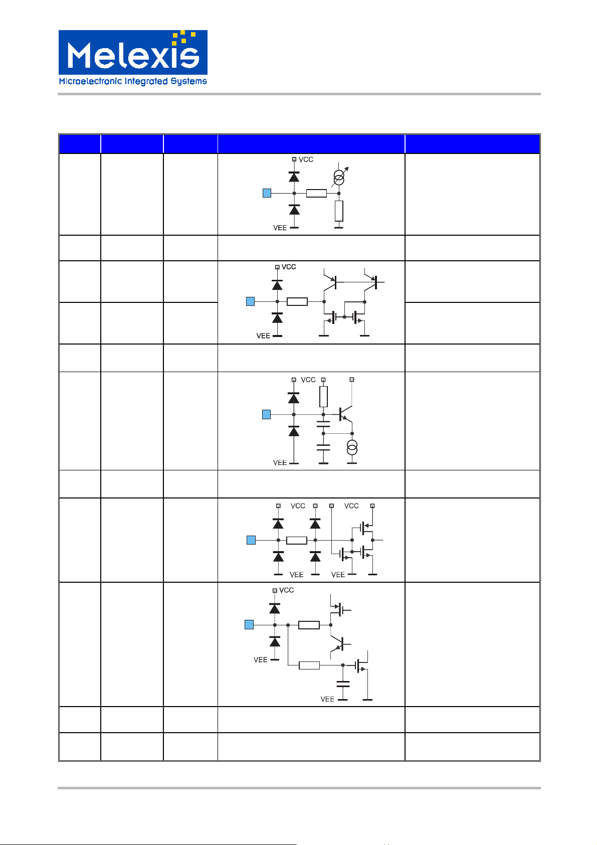
Pin No. Name I/O Type Functional Schematic Description
11 IN_IFA analog
input
VCC
IN_IFA
VCC
IFA input, approx. 2.2kΩ
input impedance
FBC1
12
IFA feedback capacitor
VEE
to be connected to external
IFA feedback capacitor
positive supply for IFA,
11
VEE
FBC2
13
VCC
VEE
2.2k
2.2k
200µA
VEE
12 FBC1 analog I/O to be connected to external
13 FBC2 analog I/O
14 VCC_IF supply
DEMOD
15 OUT_IFA analog I/O
IFA output and MIX3 input
(of DEMOD)
OUT_IFA
15
40µA
16 IN_DEM analog
input
IN_DEM
16
47k
DEMOD input, to MIX3 core
17 VCC_BIAS supply
positive supply of general
bias system and OA
18 OUT_OA analog
output
OUT_OA
Ω
50
OA output, 40uA current
drive capability
18
19 OAN analog
input
20 OAP analog
input
OAN
19
20µA
Ω
50
Ω
50
negative OA input, input
voltage limited to approx.
between pins OAP
pp
OAP
0.7 V
and OAN
negative OA input, input
20
voltage limited to approx.
0.7 V
between pins OAP
pp
and OAN
TH71111 Data Sheet Page 6 of 20 Nov. 2001
3901071111 Rev. 005
Page 7
TH71111
868/915MHz
FSK/FM/ASK Receiver
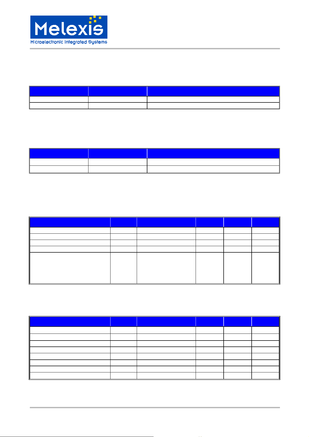
Pin No. Name I/O Type Functional Schematic Description
21 RSSI analog
output
RSSI
21
50
I (Pi)
Ω
36k
RSSI output, for RSSI and
ASK detection, approx.
36kΩ output impedance
22 VEE_BIAS ground
ground for general bias
system and OA
23 OUTP analog
output
24 OUTN analog
OUTP
OUTN
23
24
Ω
50
20µA
20µA
FSK/FM positive output,
output impedance of
100kΩ to 300kΩ
FSK/FM negative output,
output impedance of
100kΩ to 300kΩ
25 VEE_RO ground ground of dividers, PFD and
RO
26 RO analog
input
RO
26
50k
30p
30p
RO input, Colpitts type
oscillator with internal feedback capacitors
27 VCC_PLL supply positive supply of RO, DIV,
PFD and charge pump
28 ENRX digital
input
ENRX
1.5k
mode control input
(CMOS Input)
28
29 LF analog
output
LF
29
200
400
Ω
Ω
4p
charge pump output and
VCO1 control input
30 VEE_LNA ground LNA biasing ground
32 VCC_LNA supply positive supply of LNA
biasing
TH71111 Data Sheet Page 7 of 20 Nov. 2001
3901071111 Rev. 005
Page 8
Technical Data
Mode Configurations
ENRX Mode Description
0 SBY standby mode
1 ON entire chip active
Note: ENRX are pulled down internally
LNA Gain Control
TH71111
868/915MHz
FSK/FM/ASK Receiver
V
GAIN_LNA
Mode Description
< 0.8 V HIGH GAIN LNA set to high gain by voltage at GAIN_LNA
> 1.4 V LOW GAIN LNA set to low gain by voltage at GAIN_LNA
Note: hysteresis between gain modes to ensure stability
Absolute Maximum Ratings
Parameter Symbol Condition / Note Min Max
Supply voltage V
Input voltage V
Input RF level P
Storage temperature T
cc
IN
imax
STG
Electrostatic discharge ESD
0 7.0 V
- 0.3 VCC+0.3 V
no damage 10 dBm
-40 +125 °C
human body model,
MIL STD 833D
method 3015.7, all pins
except OUT_IFA
pin OUT_IFA -500 +250 V
-500
+500
Unit
V
Normal Operating Conditions
Parameter Symbol Condition Min Max Unit
Supply voltage at 868 MHz V
Supply voltage at 915 MHz V
Operating temperature T
Input frequency f
Frequency deviation
FSK data rate R
FM bandwidth f
ASK data rate R
i
∆f
m
cc, 868
cc, 915
a
FSK
ASK
fi ≤ 900 MHz
fi > 900 MHz 3.3 5.5 V
-40 +85 ºC
800 930 MHz
at FM or FSK
NRZ 40 kbit/s
NRZ 80 kbit/s
2.5 5.5 V
±5 ±120
kHz
15 kHz
TH71111 Data Sheet Page 8 of 20 Nov. 2001
3901071111 Rev. 005
Page 9
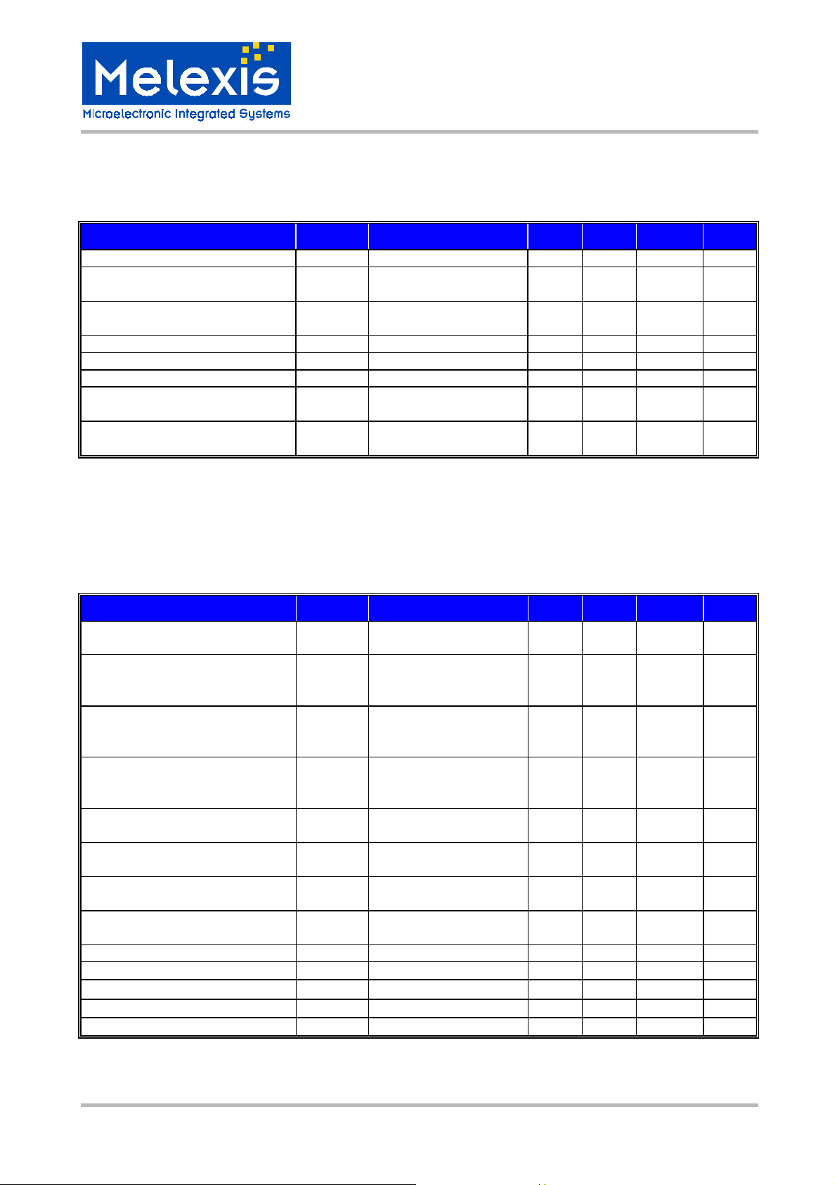
DC Characteristics
all parameters under normal operating conditions, unless otherwise stated;
typical values at T
= 23 °C and V
a
cc
= 3 V
Parameter Symbol Condition Min Typ Max Unit
Standby current I
Total supply current at low gain I
SBY
cc, low
ENRX=0 100 nA
ENRX=1,
LNA at LOW GAIN
Total supply current at high gain I
cc, high
ENRX=1,
LNA at HIGH GAIN
Opamp input offset voltage V
Opamp input offset current I
Opamp input bias current I
RSSI voltage at low input level V
offs
offs
bias
RSSI, low
I
– I
OAP
OAN
0.5 * (I
OAP
+ I
Pi = -65 dBm,
) -100 100 nA
OAN
LNA at LOW GAIN
RSSI voltage at high input level V
RSSI, high
Pi = -35 dBm,
LNA at LOW GAIN
TH71111
868/915MHz
FSK/FM/ASK Receiver
6.0 7.5 9.0 mA
7.5 9.2 11.0 mA
-20 20 mV
-50 50 nA
0.5 1.0 1.5 V
1.25 1.9 2.45 V
AC System Characteristics
all parameters under normal operating conditions, unless otherwise stated;
all parameters based on test circuits for FSK (Fig. 2), FM (Fig. 4) and ASK (Fig. 5), respectively;
typical values at T
= 23 °C and V
a
= 3 V, RF at 866.3 MHz, second IF at 10.7 MHz
cc
Parameter Symbol Condition Min Typ Max Unit
start-up time – FSK/FM T
FSK
ENRX from 0 to 1,
0.9 ms
valid data at output
start-up time – ASK T
ASK
depends on ASK
R3•C12
detector time constant,
input sensitivity – FSK
(narrow band)
input sensitivity – FSK
(wide band)
input sensitivity – ASK
(narrow band)
input sensitivity – ASK
(wide band)
maximum input signal – FSK/FM P
maximum input signal – ASK P
P
min, n
P
min, w
P
minA, n
P
minA, w
max, FM
max, ASK
valid data at output
B
= 40kHz
IF2
∆f = ±15kHz (FSK/FM)
BER ≤ 3⋅10
B
= 150kHz
IF2
∆f = ±50kHz (FSK/FM)
BER ≤ 3⋅10
B
= 40kHz
IF2
BER ≤ 3⋅10
B
= 150kHz
IF2
BER ≤ 3⋅10
BER ≤ 3⋅10
LNA at LOW GAIN
BER ≤ 3⋅10
-3
-3
-3
-3
-3
-3
-109 dBm
-102 dBm
-108 dBm
-104 dBm
0dBm
-10 dBm
T
LNA at LOW GAIN
spurious emission P
image rejection
blocking immunity
VCO gain K
Charge pump current I
∆P
∆P
CP
spur
imag
block
VCO
∆f
> ±2MHz, note 1
block
55 dB
57 dB
250 MHz/V
60 µA
-70 dBm
Notes: 1. desired signal with FSK/FM or ASK modulation, CW blocking signal
ms
+
FSK
TH71111 Data Sheet Page 9 of 20 Nov. 2001
3901071111 Rev. 005
Page 10
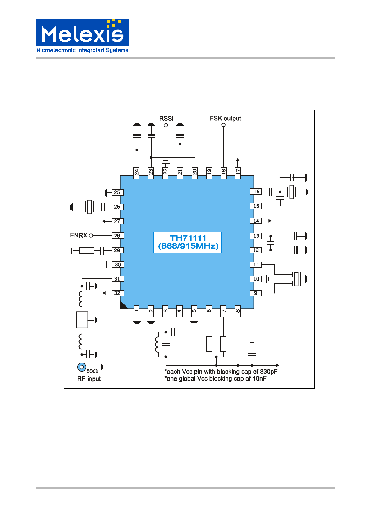
Test Circuits
FSK Reception
TH71111
868/915MHz
FSK/FM/ASK Receiver
L2
XT AL
R1
C5
VCC
C1
C3
VCC
VEE
VCC
C14
OUTN
RO
VCC
ENRX
LF
VEE
IN_LNA
VEE
OUTP
GAIN_LNA
C16C15
VEE
RSSI
LQFP32
IN_MIX1
OUT_LNA
OAP
VEE
OAN
IF1P
VCC
IN_DEM
OUT_OA
OUT_IFA
VCC
FBC2
FBC1
IN_IFA
VEE
VCC
IF1N
VCC
OUT_MIX2
C13
C12
CP
CERRES
VCC
C11
C9
C10
CERFIL
C7
C6
RL2
CB*
VCC
L1
SAWFIL
C4
L3
Fig. 2: Test circuit for FSK reception
TH71111 Data Sheet Page 10 of 20 Nov. 2001
3901071111 Rev. 005
Page 11
FSK/FM/ASK Receiver
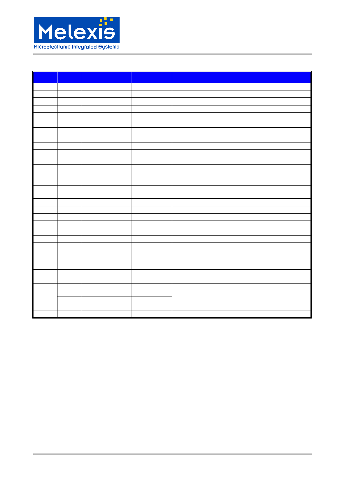
FSK test circuit component list to Fig. 2
Part Size Value / Type Tolerance Description
C1 0805 15 pF
C3 0805 1 nF
C4 0603 4.7 pF
C5 0603 2.7 pF
C6 0603 NIP
C7 0603 1.2 pF
C9 0805 33 nF
C10 0603 1 nF
C11 0603 1 nF
C12 0603 1.5 pF
C13 0603 680 pF
CP 0805 10 -12 pF
C14 0805 10 – 47 pF
C15 0805 10 – 47 pF
C16 0603 330 pF
R1 0805
RL1
RL2
L1 0603 12 nH
L2 0603 12 nH
L3 0603 6.8 nH
XTAL HC49
SAWFIL QCC8C
CERFIL
CERRES SMD type CDACV10.7MG18-A
0805
0805
SMD
leaded
type
SMD type SFECV10.7MJS-A
10 kΩ±10%
470 Ω
470 Ω
26.8000 MHz
@ RF = 868.3 MHz
B3570
@ RF = 868.3 MHz
SFE10.7MFP @
= 40 kHz
B
IF2
= 150 kHz
@ B
IF2
NIP – not in place, may be used optionally
±10%
±10%
±5%
±5%
±5%
±5%
±10%
±10%
±10%
±5%
±10%
±5%
±5%
±5%
±10%
±5%
±5%
±5%
±5%
±5%
±25ppm calibra-
tion
±30ppm temp.
B
= 1.7 MHz
3dB
TBD
±40 kHz
crystal series capacitor
loop filter capacitor
capacitor to match to SAW filter input
capacitor to match to SAW filter output
LNA output tank capacitor
MIX1 input matching capacitor
IFA feedback capacitor
IFA feedback capacitor
IFA feedback capacitor
DEMOD phase-shift capacitor
DEMOD coupling capacitor
CERRES parallel capacitor
demodulator output low-pass capacitor, depending on
data rate
demodulator output low-pass capacitor, depending on
data rate
RSSI output low-pass capacitor
loop filter resistor
MIX1 bias resistor
MIX1 bias resistor
inductor to match SAW filter
inductor to match SAW filter
LNA output tank inductor
fundamental-mode crystal, C
C
0, max
= 7 pF, R
m, max
= 50 Ω
low-loss SAW filter from EPCOS
ceramic filter from Murata
ceramic demodulator tank from Murata
TH71111
868/915MHz
= 10 pF to 15pF,
load
TH71111 Data Sheet Page 11 of 20 Nov. 2001
3901071111 Rev. 005
Page 12
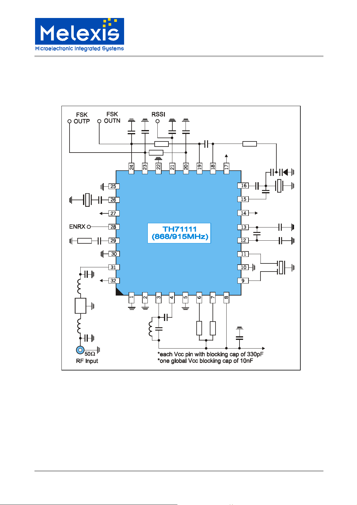
FSK Circuit with AFC and Ceramic Resonator Tolerance Compensation
TH71111
868/915MHz
FSK/FM/ASK Receiver
L2
XTAL
R1
C5
VCC
C1
C3
VCC
VEE
VCC
C14
OUTN
RO
VCC
ENRX
LF
VEE
IN_LNA
VEE
R4
OUTP
GAIN_LNA
C16C15
R5
VEE
RSSI
LQFP32
IN_MIX1
OUT_LNA
C17
OAP
VEE
C18
OAN
IF1P
VCC
IN_DEM
OUT_OA
OUT_IFA
VCC
FBC2
FBC1
IN_IFA
VEE
VCC
IF1N
R3
VCC
OUT_MIX2
C13
C12
CP VD
CERRES
VCC
C11
C9
C10
CERFIL
SAWFIL
L1
C4
L3
C7
C6
RL1
RL2
CB*
VCC
Fig. 3: Test circuit for FSK with AFC and resonator compensation
Circuit Feature
! Improves input frequency acceptance range up to RF
±50 kHz
nom
! Eliminates calibration tolerances of ceramic resonator
! Eliminates temperature tolerances of ceramic resonator
! Non-inverted and inverted CMOS-compatible outputs
TH71111 Data Sheet Page 12 of 20 Nov. 2001
3901071111 Rev. 005
Page 13
FSK/FM/ASK Receiver
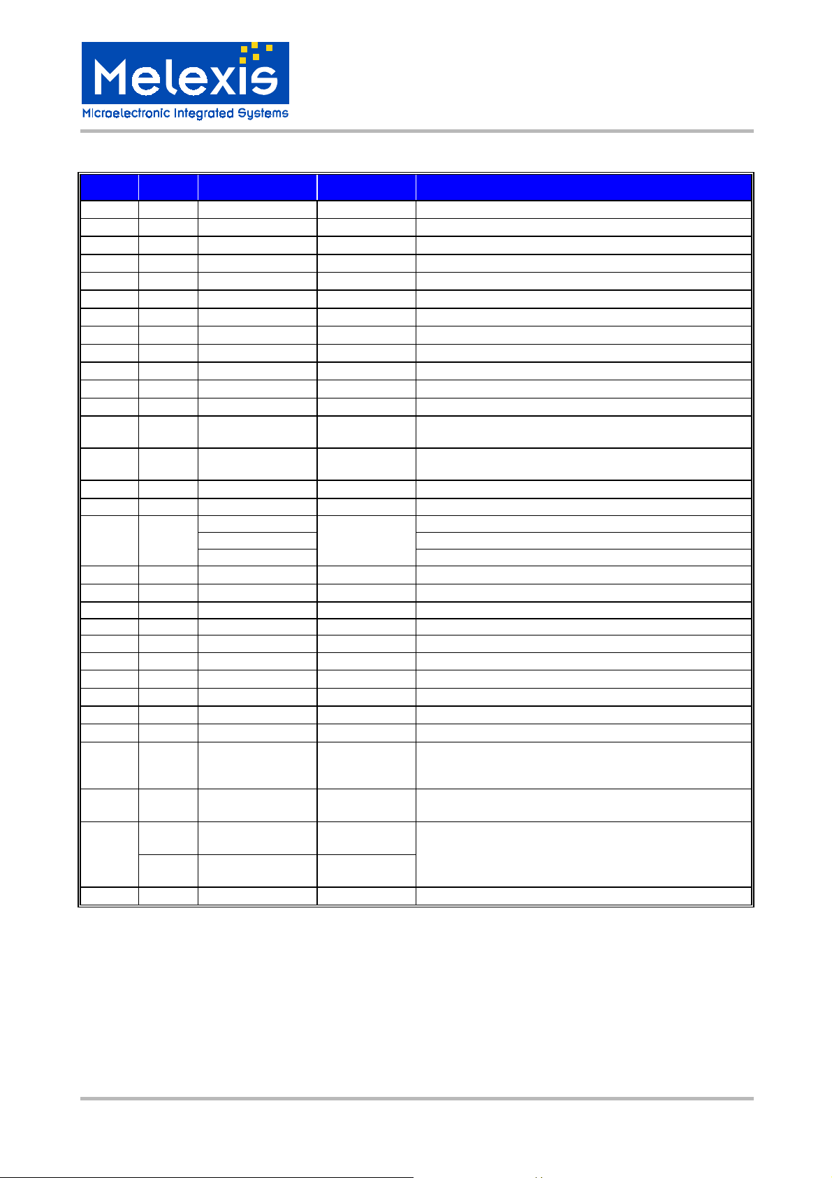
FSK test circuit with AFC component list to Fig. 3
Part Size Value / Type Tolerance Description
C1 0805 15 pF
C3 0805 1 nF
C4 0603 4.7 pF
C5 0603 2.7 pF
C6 0603 4.7 pF
C7 0603 2.2 pF
C9 0805 33 nF
C10 0603 1 nF
C11 0603 1 nF
C12 0603 1.5 pF
C13 0603 680 pF
CP 0805 27 pF
C14 0805 10 – 47 pF
C15 0805 10 – 47 pF
C16 0603 330 pF
C17 33 nF
C18 0805
R1 0805
R3
R4
R5
RL1
RL2
L1 0603 33 nH
L2 0603 33 nH
L3 0603 15 nH
VD SOD-323 BB535
XTAL HC49
SAWFIL QCC8C
CERFIL
CERRES SMD type CDACV10.7MG18-A
0805
0805
0805
0805
0805
SMD
leaded
type
SMD type SFECV10.7MJS-A
33 nF
10 nF
1 nF
10 kΩ±10%
100 kΩ
680 kΩ±10%
680 kΩ±10%
470 Ω
470 Ω
26.8000 MHz
@ RF = 868.3 MHz
B3570
@ RF = 868.3 MHz
SFE10.7MFP @
= 40 kHz
B
IF2
= 150 kHz
@ B
IF2
NIP – not in place, may be used optionally
±10%
±10%
±5%
±5%
±5%
±5%
±10%
±10%
±10%
±5%
±10%
±5%
±5%
±5%
±10%
±10%
±10%
±10%
±5%
±5%
±5%
±5%
±5%
±25ppm calibra-
tion
±30ppm temp.
B
= 1.7 MHz
3dB
TBD
±40 kHz
crystal series capacitor
loop filter capacitor
capacitor to match to SAW filter input
capacitor to match to SAW filter output
LNA output tank capacitor
MIX1 input matching capacitor
IFA feedback capacitor
IFA feedback capacitor
IFA feedback capacitor
DEMOD phase-shift capacitor
DEMOD coupling capacitor
ceramic resonator loading capacitor
demodulator output low-pass capacitor, depending on
data rate
demodulator output low-pass capacitor, depending on
data rate
RSSI output low-pass capacitor
integrator capacitor, fixed
integrator capacitor, @ 0.5 to 2 kbit/s NRZ
integrator capacitor, @ 2 to 20 kbit/s NRZ
integrator capacitor, @ 20 to 40 kbit/s NRZ
loop filter resistor
varactor diode biasing resistor
integrator resistor
integrator resistor
MIX1 bias resistor
MIX1 bias resistor
inductor to match SAW filter
inductor to match SAW filter
LNA output tank inductor
varactor diode from Infineon
fundamental-mode crystal, C
C
0, max
= 7 pF, R
m, max
= 50 Ω
low-loss SAW filter from EPCOS
ceramic filter from Murata
ceramic demodulator tank from Murata
TH71111
868/915MHz
= 10 pF to 15pF,
load
TH71111 Data Sheet Page 13 of 20 Nov. 2001
3901071111 Rev. 005
Page 14
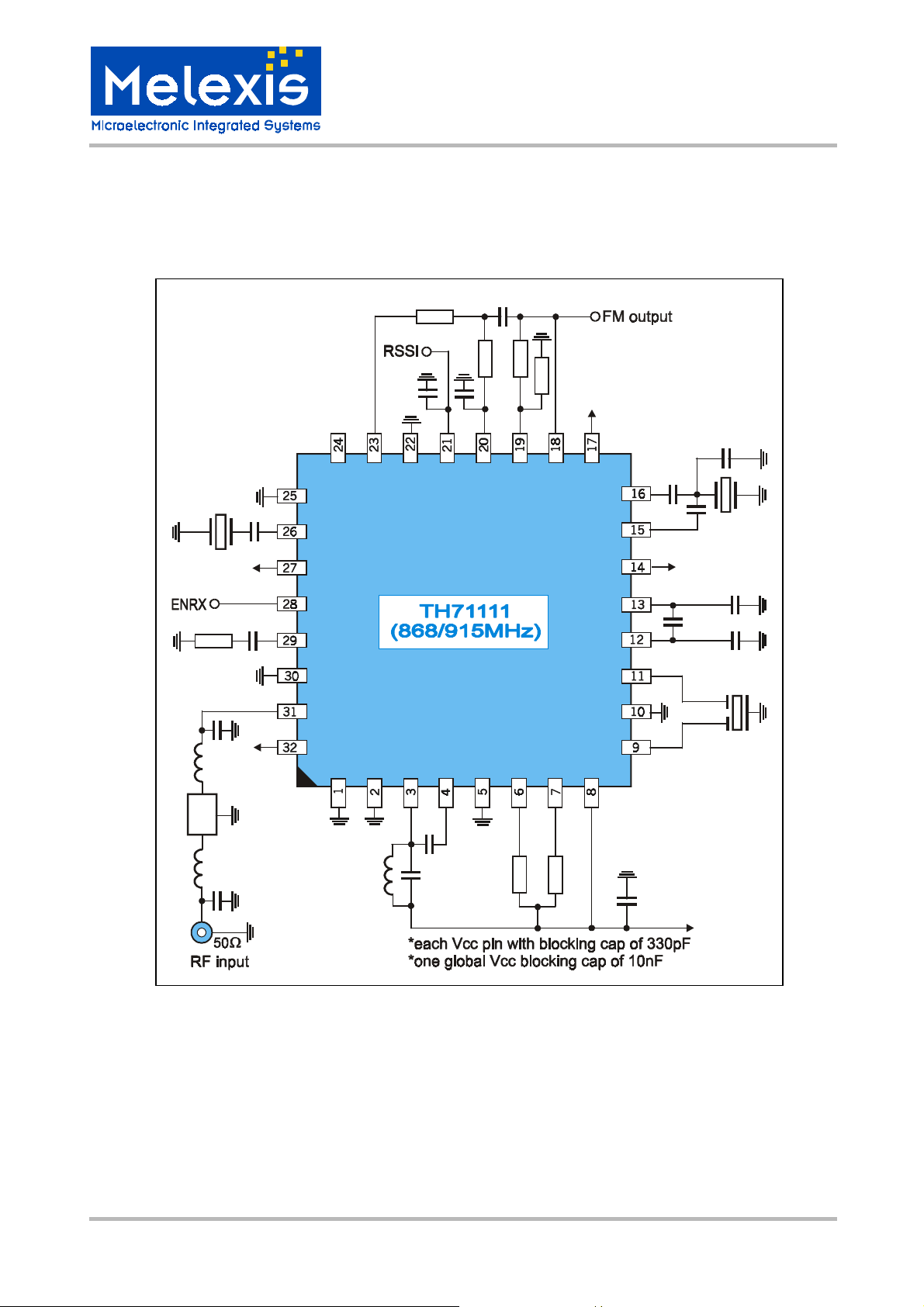
FM Reception
TH71111
868/915MHz
FSK/FM/ASK Receiver
L2
XT AL
R1
C5
VCC
C1
C3
VCC
VEE
VCC
OUTN
RO
VCC
ENRX
LF
VEE
IN_LNA
VEE
OUTP
GAIN_LNA
C16
R6
C15
VEE
RSSI
LQFP32
IN_MIX1
OUT_LNA
R5
C14
R4
OAP
VEE
OAN
IF1P
R3
VCC
IN_DEM
OUT_OA
OUT_IFA
VCC
FBC2
FBC1
IN_IFA
VEE
VCC
IF1N
VCC
OUT_MIX2
C13
C12
CP
CERRES
VCC
C11
C9
C10
CERFIL
C7
C6
RL1
RL2
CB*
VCC
L1
SAWFIL
C4
L3
Fig. 4: Test circuit for FM reception
TH71111 Data Sheet Page 14 of 20 Nov. 2001
3901071111 Rev. 005
Page 15
FSK/FM/ASK Receiver
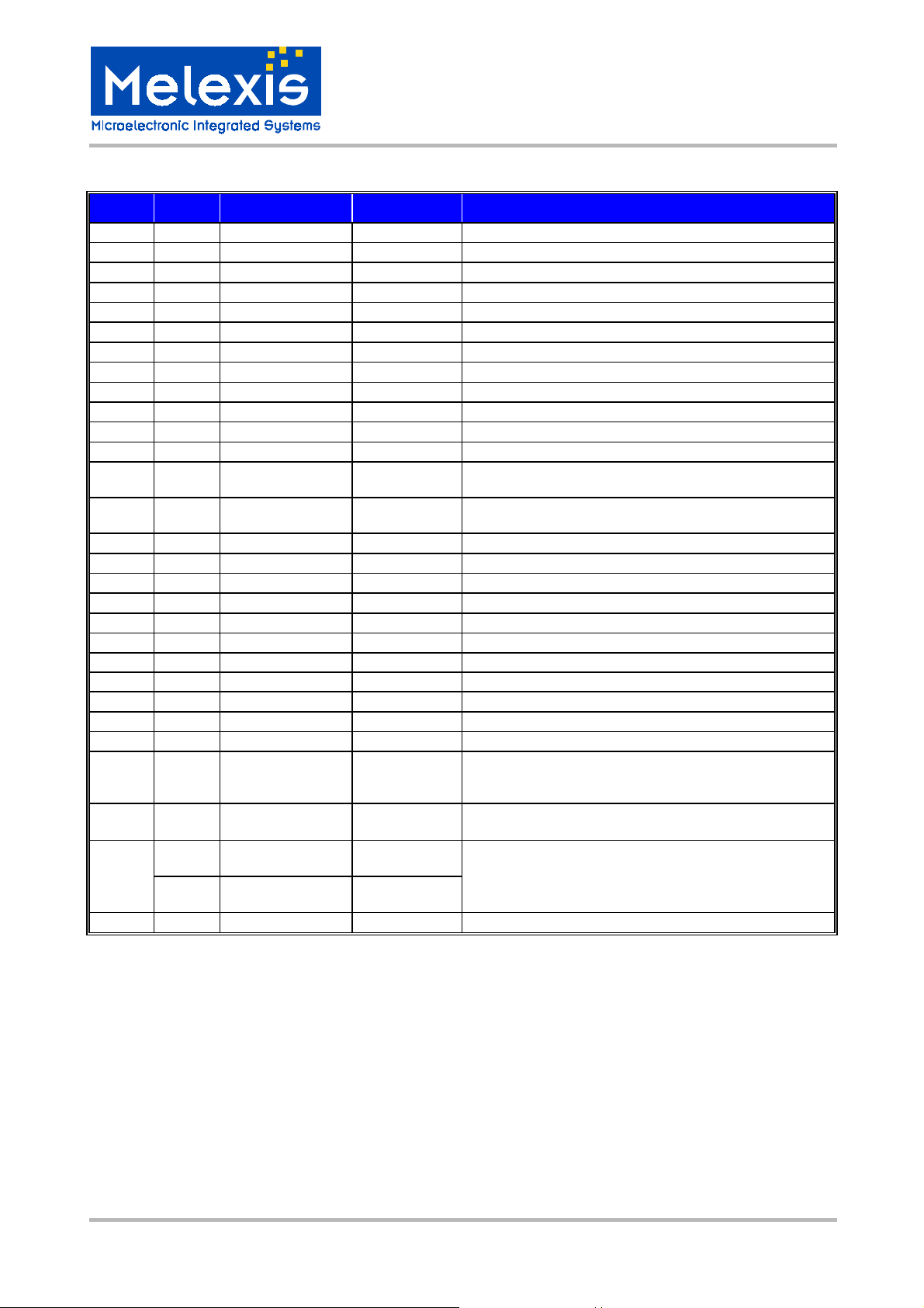
FM test circuit component list to Fig. 4
Part Size Value / Type Tolerance Description
C1 0805 15 pF
C3 0805 1 nF
C4 0603 4.7 pF
C5 0603 2.7 pF
C6 0603 4.7 pF
C7 0603 2.2 pF
C9 0805 33 nF
C10 0603 1 nF
C11 0603 1 nF
C12 0603 1.5 pF
C13 0603 680 pF
CP 0805 10 -12 pF
C14 0805 100 pF
C15 0805 100 pF
C16 0603 330 pF
R1 0805
R3 0805
R4 0805
R5 0805
R6 0805
RL1
RL2
L1 0603 33 nH
L2 0603 33 nH
L3 0603 15 nH
XTAL HC49
SAWFIL QCC8C
CERFIL
CERRES SMD type CDACV10.7MG18-A
0805
0805
SMD
leaded
type
SMD type SFECV10.7MJS-A
10 kΩ±10%
12 kΩ±5%
6.8 kΩ±5%
33 kΩ±5%
33 kΩ±5%
470 Ω
470 Ω
26.8000 MHz
@ RF = 868.3 MHz
B3570
@ RF = 868.3 MHz
SFE10.7MFP @
= 40 kHz
B
IF2
= 150 kHz
@ B
IF2
NIP – not in place, may be used optionally
±10%
±10%
±5%
±5%
±5%
±5%
±10%
±10%
±10%
±5%
±10%
±5%
±5%
±5%
±10%
±5%
±5%
±5%
±5%
±5%
±25ppm calibra-
tion
±30ppm temp.
B
= 1.7 MHz
3dB
TBD
±40 kHz
crystal series capacitor
loop filter capacitor
capacitor to match to SAW filter input
capacitor to match to SAW filter output
LNA output tank capacitor
MIX1 input matching capacitor
IFA feedback capacitor
IFA feedback capacitor
IFA feedback capacitor
DEMOD phase-shift capacitor
DEMOD coupling capacitor
CERRES parallel capacitor
sallen-Key low-pass filter capacitor, to set cut-off fre-
quency
sallen-Key low-pass filter capacitor, to set cut-off fre-
quency
RSSI output low-pass capacitor
loop filter resistor
sallen-Key filter resistor, to set desired filter characteristic
sallen-Key filter resistor, to set desired filter characteristic
sallen-Key filter resistor, to set cut-off frequency
sallen-Key filter resistor, to set cut-off frequency
MIX1 bias resistor
MIX1 bias resistor
inductor to match SAW filter
inductor to match SAW filter
LNA output tank inductor
fundamental-mode crystal, C
C
0, max
= 7 pF, R
m, max
= 50 Ω
low-loss SAW filter from EPCOS
ceramic filter from Murata
ceramic demodulator tank from Murata
TH71111
868/915MHz
= 10 pF to 15pF,
load
TH71111 Data Sheet Page 15 of 20 Nov. 2001
3901071111 Rev. 005
Page 16
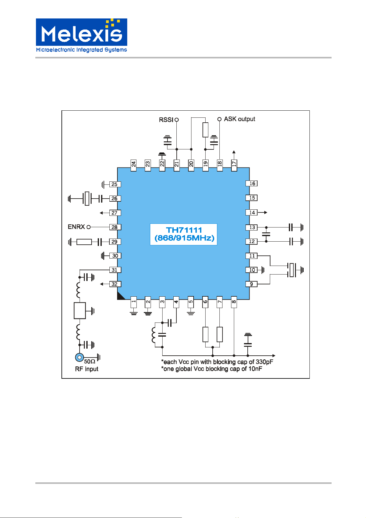
ASK Reception
TH71111
868/915MHz
FSK/FM/ASK Receiver
R3
C13
L2
C12
VEE
XT AL
C1
VCC
C3
R1
VCC
C5
VCC
SAWFIL
OUTN
RO
VCC
ENRX
LF
VEE
IN_LNA
VEE
VEE
OUTP
RSSI
OAN
OAP
LQFP32
VEE
OUT_LNA
IN_MIX1
C7
GAIN_LNA
IF1P
VCC
IN_DEM
OUT_OA
OUT_IFA
VCC
FBC2
FBC1
IN_IFA
VEE
VCC
IF1N
VCC
VCC
C11
C9
C10
CERFIL
OUT_MIX2
L1
C4
L3
C6
RL1
RL2
CB*
VCC
Fig. 5: Test circuit for ASK reception
TH71111 Data Sheet Page 16 of 20 Nov. 2001
3901071111 Rev. 005
Page 17
FSK/FM/ASK Receiver
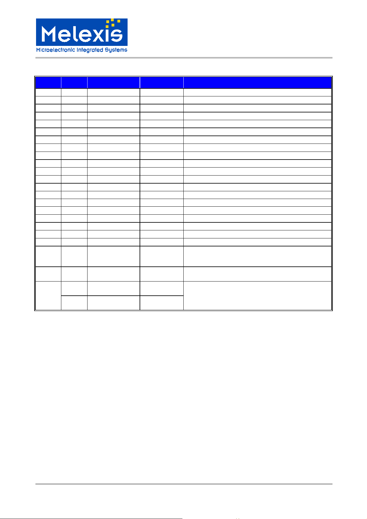
ASK test circuit component list to Fig. 5
Part Size Value / Type Tolerance Description
C1 0805 15 pF
C3 0805 1 nF
C4 0603 4.7 pF
C5 0603 2.7 pF
C6 0603 4.7 pF
C7 0603 2.2 pF
C9 0805 33 nF
C10 0603 1 nF
C11 0603 1 nF
C12 0805 1 nF to 10 nF
C13 0603 330 pF
R1 0805
R3 0603
RL1
RL2
L1 0603 33 nH
L2 0603 33 nH
L3 0603 15 nH
L4 0603 100 nH
L5 0603 100 nH
XTAL HC49
SAWFIL QCC8C
CERFIL
0805
0805
SMD
leaded
type
SMD type SFECV10.7MJS-A
10 kΩ±10%
100 kΩ±5%
470 Ω
470 Ω
26.8000 MHz
@ RF = 868.3 MHz
B3570
@ RF = 868.3 MHz
SFE10.7MFP @
= 40 kHz
B
IF2
= 150 kHz
@ B
IF2
NIP – not in place, may be used optionally
±10%
±10%
±5%
±5%
±5%
±5%
±10%
±10%
±10%
±10%
±10%
±5%
±5%
±5%
±5%
±5%
±5%
±5%
±25ppm calibra-
tion
±30ppm temp.
B
= 1.7 MHz
3dB
TBD
±40 kHz
crystal series capacitor
loop filter capacitor
capacitor to match to SAW filter input
capacitor to match to SAW filter output
LNA output tank capacitor
MIX1 input matching capacitor
IFA feedback capacitor
IFA feedback capacitor
IFA feedback capacitor
ASK data slicer capacitor, depending on data rate
RSSI output low-pass capacitor
loop filter resistor
ASK data slicer resistor, depending on data rate
MIX1 bias resistor
MIX1 bias resistor
inductor to match SAW filter
inductor to match SAW filter
LNA output tank inductor
IF1 tank inductor
IF1 tank inductor
fundamental-mode crystal, C
C
0, max
= 7 pF, R
m, max
= 50 Ω
low-loss SAW filter from EPCOS
ceramic filter from Murata
TH71111
868/915MHz
= 10 pF to 15pF,
load
TH71111 Data Sheet Page 17 of 20 Nov. 2001
3901071111 Rev. 005
Page 18
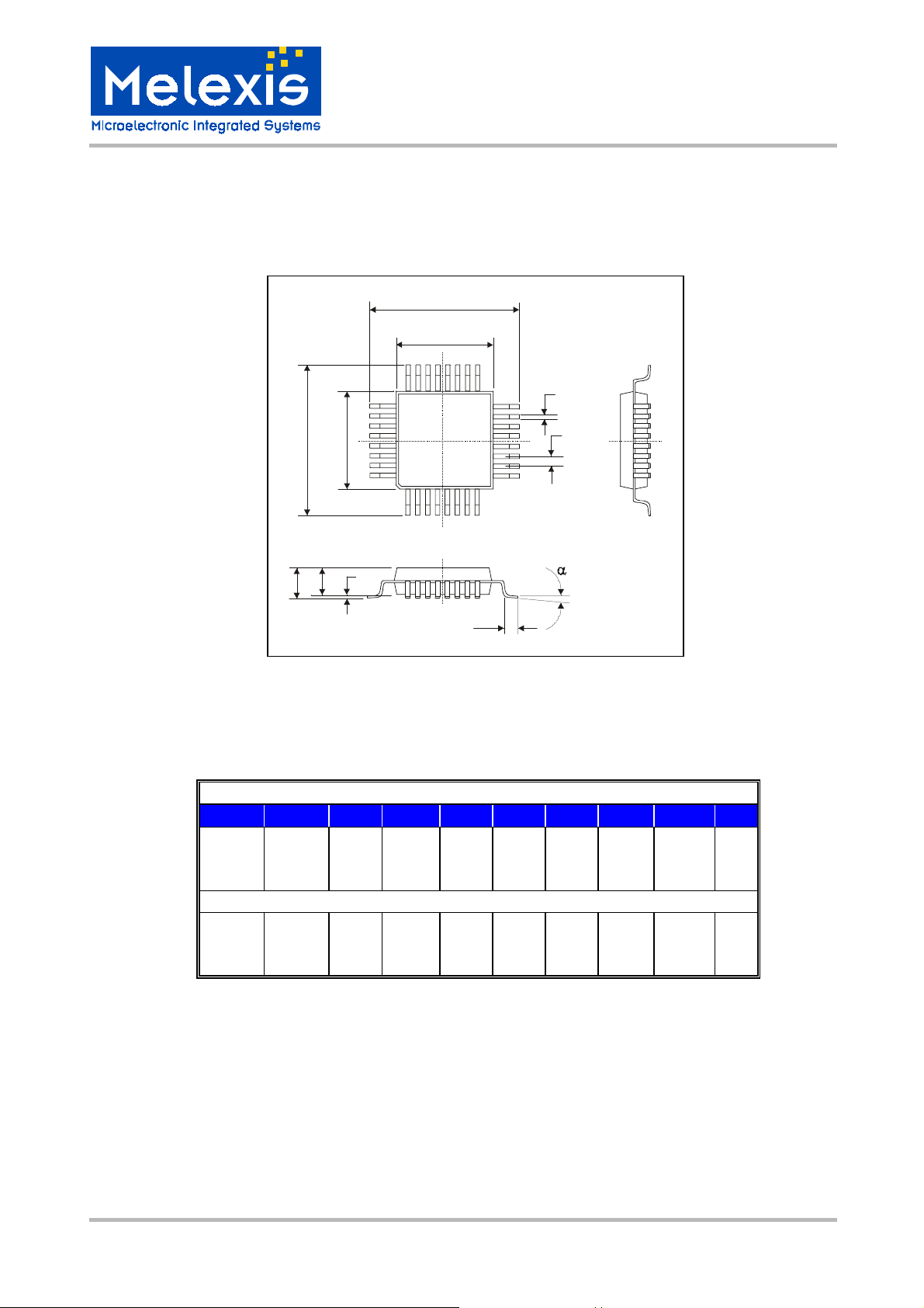
Package Dimensions
TH71111
868/915MHz
FSK/FM/ASK Receiver
D
D1
1724
b
25
16
E
E1
32
1
A1A2A
8
L
e
9
Fig. 6: LQFP32 (Low Quad Flat Package)
All Dimension in mm, coplanaríty < 0.1mm
E1, D1 A A1 A2 e b L E, D
min 0.05 1.35 0.30 0.45 0°
7.00 0.8 9.00
max 1.60 0.15 1.45 0.45 0.75 7°
All Dimension in inch, coplanaríty < 0.004”
min 0.002 0.053 0.012 0.018 0°
0.276 0.031 0.354
max 0.630 0.006 0.057 0.018 0.030 7°
αααα
TH71111 Data Sheet Page 18 of 20 Nov. 2001
3901071111 Rev. 005
Page 19

Your Notes
TH71111
868/915MHz
FSK/FM/ASK Receiver
TH71111 Data Sheet Page 19 of 20 Nov. 2001
3901071111 Rev. 005
Page 20

Your Notes
TH71111
868/915MHz
FSK/FM/ASK Receiver
Important Notice
Devices sold by Melexis are covered by the warranty and patent indemnification provisions appearing in its Term of Sal e. Melexis makes no warranty, express, statutory, implied, or by description regarding the information set forth herein or regarding the freedom of the described devi ces from patent infringement. Melexis reserves the right to change specifications and prices at any time and without notice. Therefore, prior to designing this product into a system, it
is necessary to check with Melexis for current information. This product is intended for use in normal com mercial applications. Applications requi ring extended temperature range, unusual environmental requirements, or high reliability applications, such as military, medical life- support or life-sustaining equi pment are specifically not recommended without additional processing by Melexis for each application.
The information furnished by Melexis is believed to be correct and accurate. However, Melexis shall not be liable to recipient or any third party for any damages, including but not limited to personal injury, property damage, loss of profits, loss of use, interrupt of business or indirect, special incidental or consequential damages, of any kind, in connection with or arising out of the furnishing, performance or use of the technical data herein. No obligation or liability to
recipient or any third party shall arise or flow out of Melexis’ rendering of technical or other services.
© 2000 Melexis GmbH. All rights reserved.
For the latest version of thi s document. Go to our website at
www.melexis.com
Or for additional informat i on contact Melexis Direct:
Europe and Japan: All other locations:
Phone: +32 1361 1631 Phone: +1 603 223 2362
QS9000, VDA6.1 and ISO14001 Certified
TH71111 Data Sheet Page 20 of 20 Nov. 2001
3901071111 Rev. 005
 Loading...