

Page 1
T R I Q U I N T S E M I C O N D U C T O R , I N C .
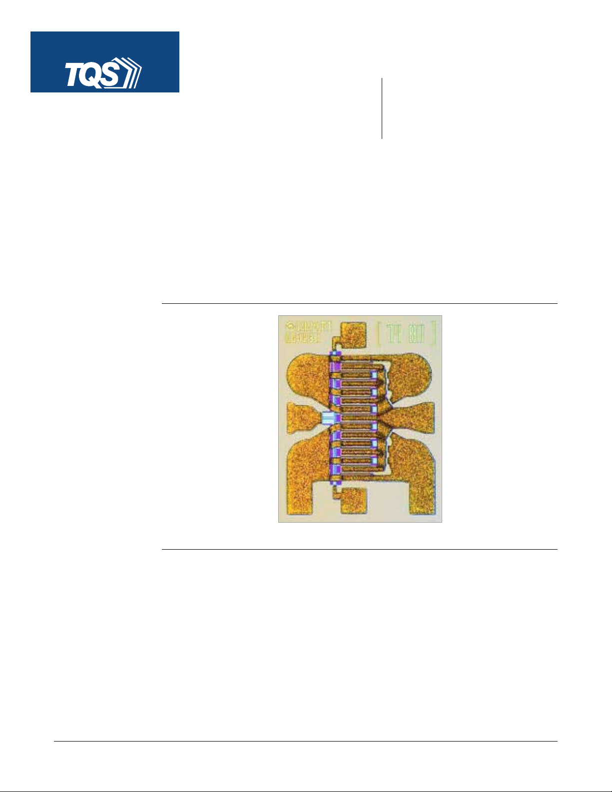
TGF4230-EEU Discr
1200 µm X 0.5 µm HFET
●
Nominal Pout of 28.5-dBm at 8.5-GHz
●
Nominal Gain of 10.0- dB at 8.5-GHz
●
Nominal PAE of 55% at 8.5 - GHz
●
Suitable for High-Reliability Applications
●
0,572 x 0,699 x 0,102 mm (0.023 x 0.028 x 0.004 in.)
●
PHOTO ENLARGEMENT
1.2mm ete HFET
4230
DESCRIPTION
TriQuint Semiconductor, Inc. • Texas Facilities • (972) 995-8465
The Triquint TGF4230 -EEU is a single gate 1.2 mm Discrete GaAs Heterostructure Field
Ef fect Transistor (HFET) designed for high- efficiency power applications up to 1 2- GHz in Class A and
Class AB operation.
Bond - pad and backside metalization is gold plated for compatibility with eutectic alloy attach methods
as well as thermocompression and thermosonic wire- bonding processes. The TGF4230-EEU is
readily assembled using automatic equipment.
• www.triquint.com
Page 2
TGF4230-EEU
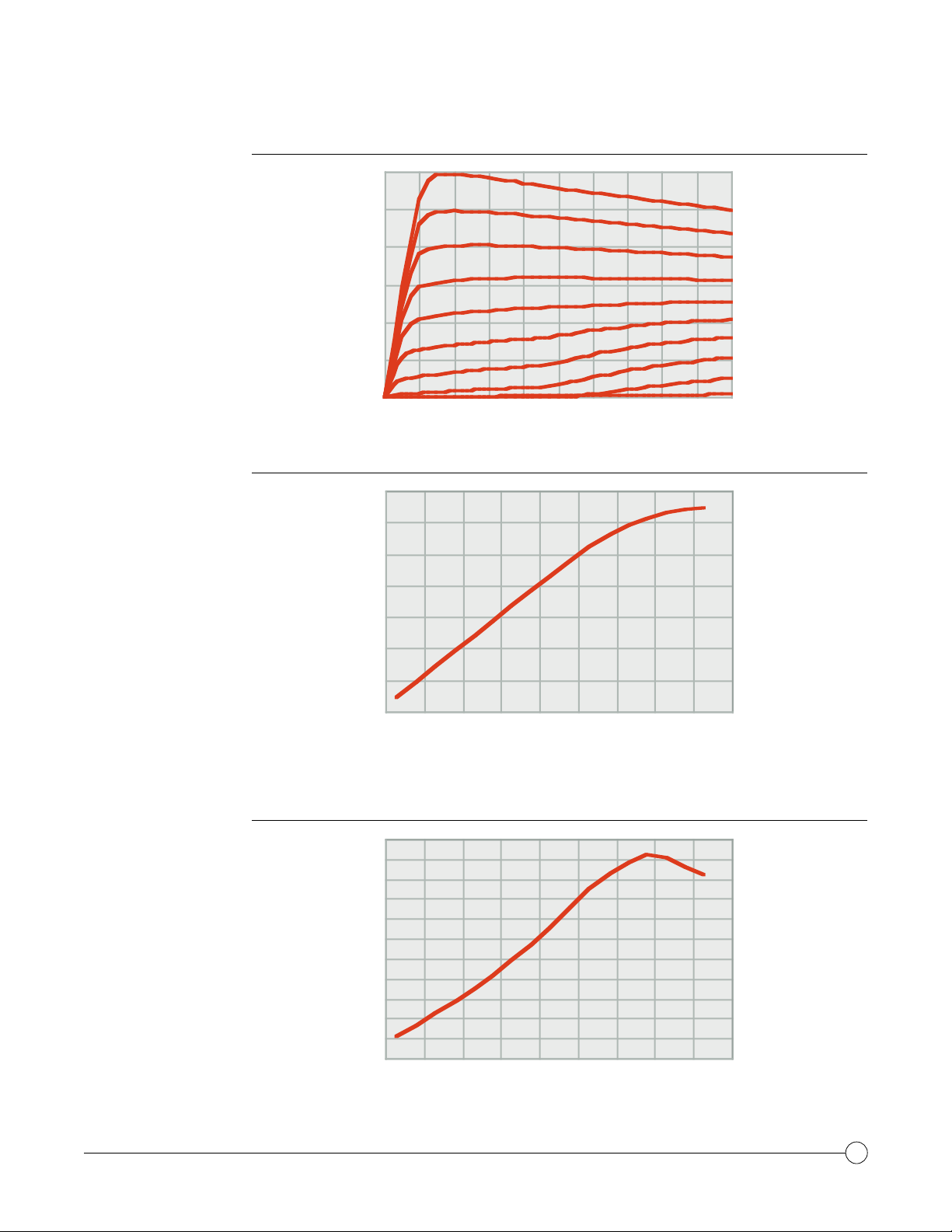
EXAMPLE OF
DC I-V CURVES
OUTPUT POWER VS.
INPUT POWER
0.3
0.25
0.2
0.15
0.1
Drain Current (A)
0.05
0
012345678910
Drain Voltage (V)
30
28
26
24
22
VG= 0.0 to -2.25 V
(0.25 V steps)
= 25°C
T
A
F = 8.5GHz
VD=8.0V
=50mA*
I
Q
=25°C
T
A
POWER ADDED
EFFICIENCY VS.
INPUT POWER
20
Output Power (dBm)
18
16
4 6 8 10 12 14 16 18 20 22
Input Power (dBm)
Note: IQ is defined as the drain current before application of RF signal at the input.
60
55
50
45
40
35
30
PAE (%)
25
20
15
10
5
4 6 8 10 12 14 16 18 20 22
Input Power (dBm)
F = 8.5GHz
VD=8.0V
=50mA*
I
Q
=25°C
T
A
TriQuint Semiconductor, Inc. • Texas Facilities • (972) 995-8465
• www.triquint.com
2
Page 3
TGF4230-EEU
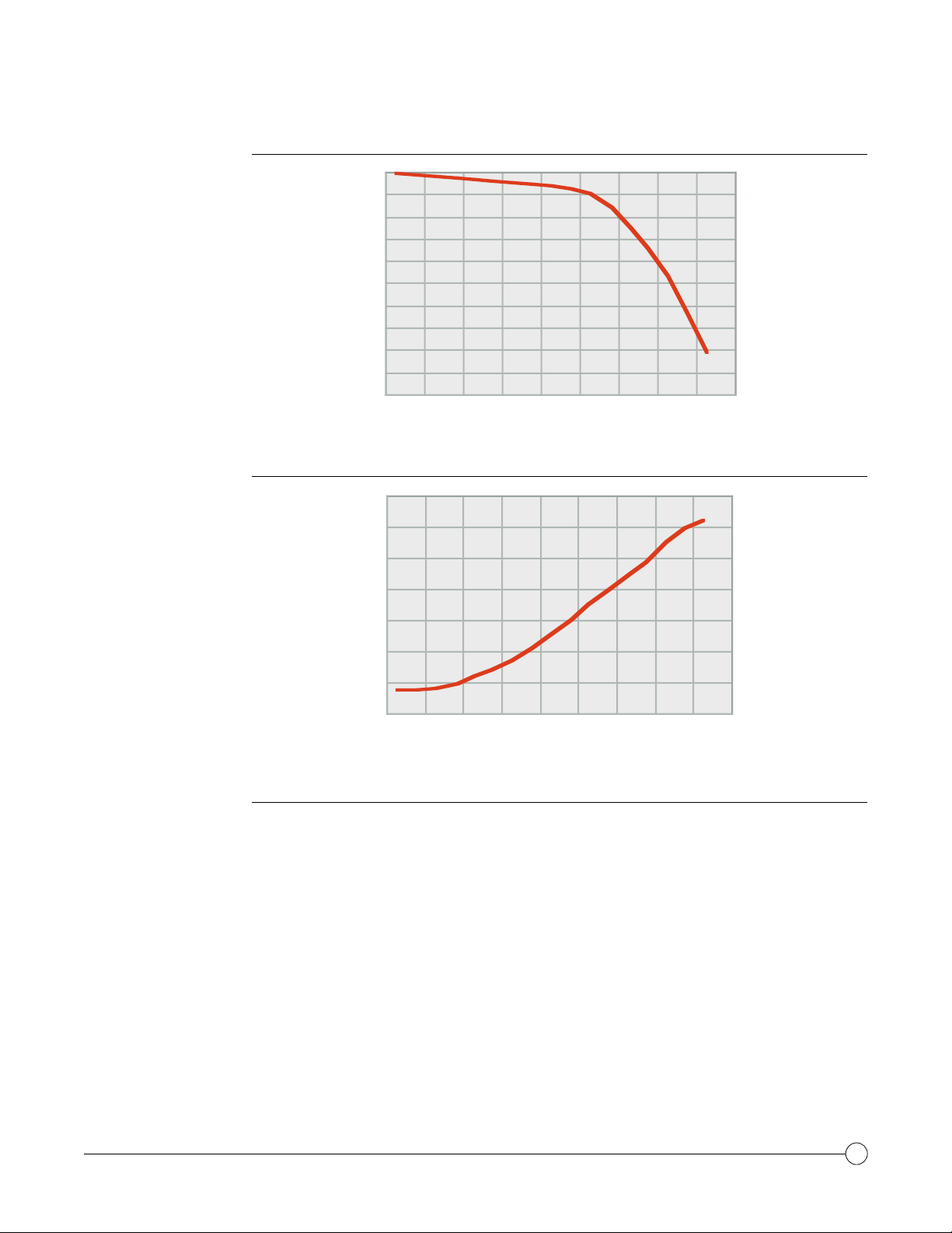
GAIN VS.
INPUT POWER
DRAIN CURRENT
VS. INPUT POWER
12
11
10
Gain (dB)
9
8
7
4 6 8 10 12 14 16 18 20 22
Input Power (dBm)
180
160
140
120
100
F =8.5GHz
VD=8.0V
=50mA*
I
Q
=25°C
T
A
F =8.5GHz
VD=8.0V
=50mA*
I
Q
=25°C
T
A
ABSOLUTE
MAXIMUM RATINGS
80
Drain Current (mA)
60
40
4 6 8 10121416182022
Input Power (dBm)
Drain - to- source V oltage, V
. ................................................................................................................ 12 V
DS
Gate - to- source V oltage, VGS......................................................................................................-5 V to 0 V
Mounting temperature (30 sec), T
Storage temperature range, T
.................................................................................................. 320 C
M
............................................................ ................................-65 to 200 C
STG
Power dissipation, PD.................................................................................. (see thermal data on next page)
Operating channel temperature, TCH.............................................................. (see thermal data on next page)
Ratings over base-plate temperature range TBP(unless otherwise noted)
Stresses beyond those listed under “Absolute Maximum Ratings” may cause permanent damage to the device.
These are stress ratings only, and functional operation of the device at these or any other conditions beyond
those indicated “RF and DC Characteristics” is not implied. Exposure to absolute maximum rated conditions for
extended periods of time may affect device reliability.
TriQuint Semiconductor, Inc. • Texas Facilities • (972) 995-8465
• www.triquint.com
3
Page 4

p
p
TGF4230-EEU
PREDICTED CHANNEL
TEMPERA TURE VS.
BASE TEMPERATURE
at 0.51 W and 1.02 W
dissipated power
HFET CHANNEL
TEMPERATURE VS.
MEDIAN LIFE
300
250
200
150
100
50
0
Channel Temperature (° C)
-50
-100
-100 -50 0 50 100 150 200
0.51 W (soldered to carrier)
0.51 W (HFET backside metal)
1.02 W (soldered to carrier)
1.02 W (HFET backside metal)
Base Temperature (° C)
Case 1: Base temperature at backside of carrier (with 38 m AuSn solder attach to 0.5 mm CuMo Car rier).
Case 2: Base temperature at backside of 1.2 mm HFET .
325
300
275
250
225
200
175
150
Channel Temperature (° C)
125
100
12345678910
11415 years
Median Life (10^X Hours)
TriQuint Semiconductor, Inc. • Texas Facilities • (972) 995-8465
4
• www.triquint.com
Page 5

TGF4230-EEU
RF AND DC
CHARACTERISTICS
PARAMETER MIN NOMINAL MAX UNIT
Pout Output Power 27.5 28.5 - dBm
G
P
Power Gain 8 10 - dB
PAE Power Added Efficiency 50 55 - %
I
G
V
BV
BV
D S S
M
P
G S
G D
Drain Saturation Current 204 294 384 mA
Transconductance 144 198 252 mS
Pinch Off Voltage -2.7 -1.85 - 1 V
Breakdown Voltage Gate-Source -30 - 22 -17 V
Breakdown Voltage Gate-Drain -30 - 22 -17 V
Pout, Gain, and PAE: Measur ed at 8.5 GHz, drain voltage of 8.0 V . Gate voltage is adjusted to achieve
quiescent current of approximately 20% I
with no RF signal applied. The source is grounded. Input power
DSS
between 18 and 19-dBm.
I
: Saturated drain-source current. Search for the maximum IDSat VGS= 0.0 V, and VDSswept between 0.5 V
DSS
to 3.5 V. Note that the drain voltage at which I
G
: Transconductance. (I
M
technique; V
V
: Pinch off voltage. VGSfor IDS= 0.5 mA/mm of gate width. VDSfixed at 2.0 V, VGSswept to bring IDSto
P
swept between 0.5 V and V
DS
0.5 mA/mm. Sweep will stop if V
BV
: Breakdown voltage, gate to source. IBD= 1.0 mA/mm of gate width. Source fixed at ground, drain not
GS
DSS
- I
)/ IVG1I. I
DS1
DSP
current not found beyond 0.5 V of the minimum VPspecification.
P
connected (floating). When 1.0mA/mm drawn at gate, V
BV
: Breakdown voltage, gate to drain. I
GD
connected (floating). When 1.0 mA/mm drawn at the gate, V
is located and recorded as V
DSS
measured at VG1= -0.25 V using the knee search
DS1
to search for maximum I
measured as B VGS.
GS
= 1.0 mA/mm of gate width. Drain fixed at gr ound, source not
BD
measured as B VGD.
GD
DS1
.
DSP
.
LINEAR MODEL
L
G
G
FET Elements
LG = 0.0421 nH
R
= 0.43
G
R
= 81700
GS
R
= 1.21
I
C
= 1.21 pF
GS
C
= 0.1004 pF
DG
R
G
R
R
GS
C
VDS= 8.0 V and 30% I
I
GS
R
DG
R
1
R
S
L
S
= 204000
R
DG
R
= 0.4
S
L
= 0.015 nH
S
R
= 98.01
DS
C
= 0.25325 pF
DS
R
= 0.66
D
L
= 0.022 nH
D
C
DG
V
CCS
R
2
at T = 25°C
DSS
R
D
C
DS
R
DS
VCCS Parameters
M = 132.9 mS
A = 0
R1 = 1E19
R2 = 1E19
F = 0
T = 5.49 pS
L
D
D
TriQuint Semiconductor, Inc. • Texas Facilities • (972) 995-8465
• www.triquint.com
5
Page 6

TGF4230-EEU
MODELED S-PARAMETERS
Frequency S
(GHz) MAG ANG(o) MAG ANG( MAG ANG(o) MAG ANG(o)
11
S
21
o
)
S
12
S
22
0.5 0.985 -29.88 8.095 161.49 0.021 72.66 0.343 -22.22
1.0 0.959 -56.20 7.297 145.18 0.038 58.80 0.328 -41.75
1.5 0.931 -77.47 6.368 131.86 0.050 47.65 0.312 -57.46
2.0 0.908 -94.02 5.512 121.22 0.057 39.12 0.301 -69.57
2.5 0.891 -106.82 4.791 112.62 0.062 32.60 0.295 -78.80
3.0 0.880 -116.82 4.202 105.49 0.065 27.55 0.294 -85.89
3.5 0.871 -124.76 3.723 99.42 0.067 23.56 0.297 -91.41
4.0 0.865 -131.19 3.330 94.11 0.068 20.34 0.302 -95.80
4.5 0.861 -136.48 3.004 89.37 0.069 17.70 0.309 -99.38
5.0 0.858 -140.92 2.732 85.06 0.069 15.51 0.319 -102.37
5.5 0.856 -144.69 2.501 81.09 0.069
6.0 0.855 -147.94 2.304 77.39 0.068
6.5 0.854 -150.78 2.133 73.90 0.068
13.67 0.329 -104.94
12.12 0.340 -107.18
10.82 0.352 -109.19
7.0 0.854 -153.29 1.984 70.59 0.067 9.72 0.364 -111.03
7.5 0.854 -155.53 1.852 67.43 0.066 8.80 0.377 -112.73
8.0 0.855 -157.54 1.736 64.40 0.065 8.05 0.390 -114.32
8.5 0.855 -159.37 1.632 61.49 0.065 7.45 0.404 -115.84
9.0 0.856 -161.04 1.539 58.67 0.064 7.00 0.417 -117.29
9.5 0.857 -162.58 1.455 55.95 0.063 6.68 0.430 -118.68
10.0 0.858 -164.01 1.378 53.30 0.061 6.49 0.444 -120.03
10.5 0.859 -165.34 1.308 50.73 0.060 6.43 0.457 -121.35
11.0 0.860 -166.58 1.244 48.23 0.059 6.51 0.470 -122.63
11.5 0.862 -167.76 1.186 45.79 0.058 6.71 0.483 -123.89
12.0 0.863 -168.87 1.131 43.41 0.057 7.05 0.496 -125.11
12.5 0.864 -169.93 1.081 41.09 0.056 7.52 0.509 -126.32
13.0 0.866 -170.94 1.034 38.83 0.055 8.12 0.521 -127.51
13.5 0.867 -171.91 0.991 36.62 0.053 8.86 0.534 -128.68
14.0 0.869 -172.84 0.950 34.46 0.052 9.74 0.546 -129.82
VDS= 8.0 V and 30% I
at T = 25°C
DSS
TriQuint Semiconductor, Inc. • Texas Facilities • (972) 995-8465
• www.triquint.com
6
Page 7

TGF4230-EEU
MECHANICAL DRAWING
0.699
0.601
0.350
0.099
0.0
0.0 0.097 0.264 0.572
1
2
3
R/C**
4
0.471
NOTES
Units: Millimeters
Thickness: 0.102
Chip size ± 0.0508
Bond pad 1 (gate): 0.072 x 0.075
Bond pad 2 (gate): 0.075 x 0.075*
Bond pad 3 (gate): 0.075 x 0.075*
Bond pad 4 (drain): 0.083 x 0.077
Minimum connections to Bond Pads 1 and 4. Sources are connected to backside metalization.
* Alternate gate pads used for paralleling TGF4230s or for multiple gate wires.
** Wafer unique Row/Column data is r ecorded in brackets.
Gate bias supplies should be designed to sink or source gate current. The magnitude and direction of the gate
current is a function of bias point, load impedance, and drive level.
TriQuint Semiconductor, Inc. • Texas Facilities • (972) 995-8465
• www.triquint.com
7
 Loading...