

Page 1
18 mm Discrete HFETTGF4118-EPU
4118
• 0.5 um gate finger length
• Nominal Pout of 9.0 Watts at 2.3 GHz
• Nominal PAE of 53% at 2.3 GHz
• Nominal Gain of 11.5 dB at 2.3 GHz
• Die Size 36.0 x 81.0 x 4.0 mils
(0.914 x 2.057 x 0.102 mm)
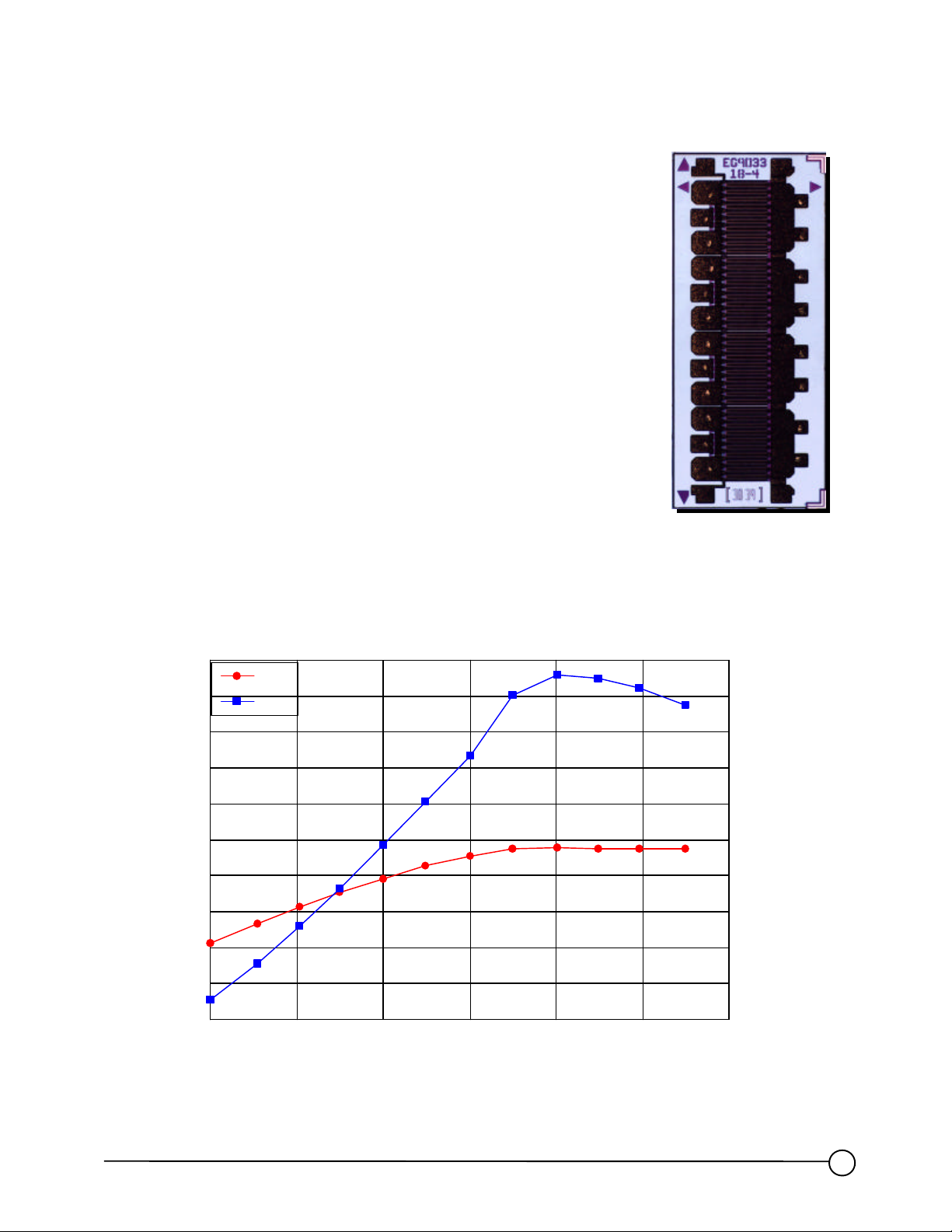
TGF4118-EPU RF Performance at F = 2.3 GHz
Vd = 8.0 V, Vg = -1.1 V, Iq = 1.69 A and TA = 25°C
50
Pout
48
46
44
42
40
38
36
Output Power (dBm)
34
32
30
20 22 24 26 28 30 32
PAE
55
50
45
40
35
30
25
Power Added Efficiency %
20
15
Input Power (dBm)
TriQuint Semiconductor Texas Phone: 972 994-8465 Fax 972 994-8504 Web: www.triquint.com
1
Page 2
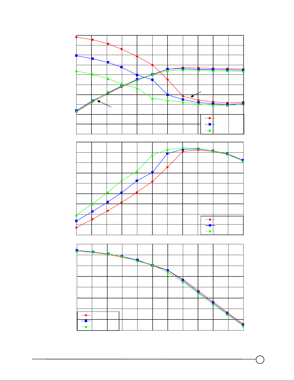
TGF4118-EPU RF Performance for Vd = 7.0 V, F = 2.3 GHz, and TA = 25°C
Quiescent Id is 1.74 A (Vg = -1.1 V), 1.37 A (Vg = -1.3 V), and 1.02 A (Vg = -1.5 V)
130
120
110
100
90
80
70
60
Pout
50
Predicted Channel Temp (°C)
40
30
60
55
50
45
Tch
Vg = -1.1 V
Vg = -1.3 V
Vg = -1.5 V
42
41
40
39
38
37
36
35
Output Power (dBm)
34
33
32
40
35
30
25
Power Added Efficiency %
20
15
15
14
13
12
11
Gain (dB)
10
9
8
7
20 21 22 23 24 25 26 27 28 29 30 31
Vg = -1.1 V
Vg = -1.3 V
Vg = -1.5 V
Input Power (dBm)
Vg = -1.1 V
Vg = -1.3 V
Vg = -1.5 V
TriQuint Semiconductor Texas Phone: 972 994-8465 Fax 972 994-8504 Web: www.triquint.com
2
Page 3
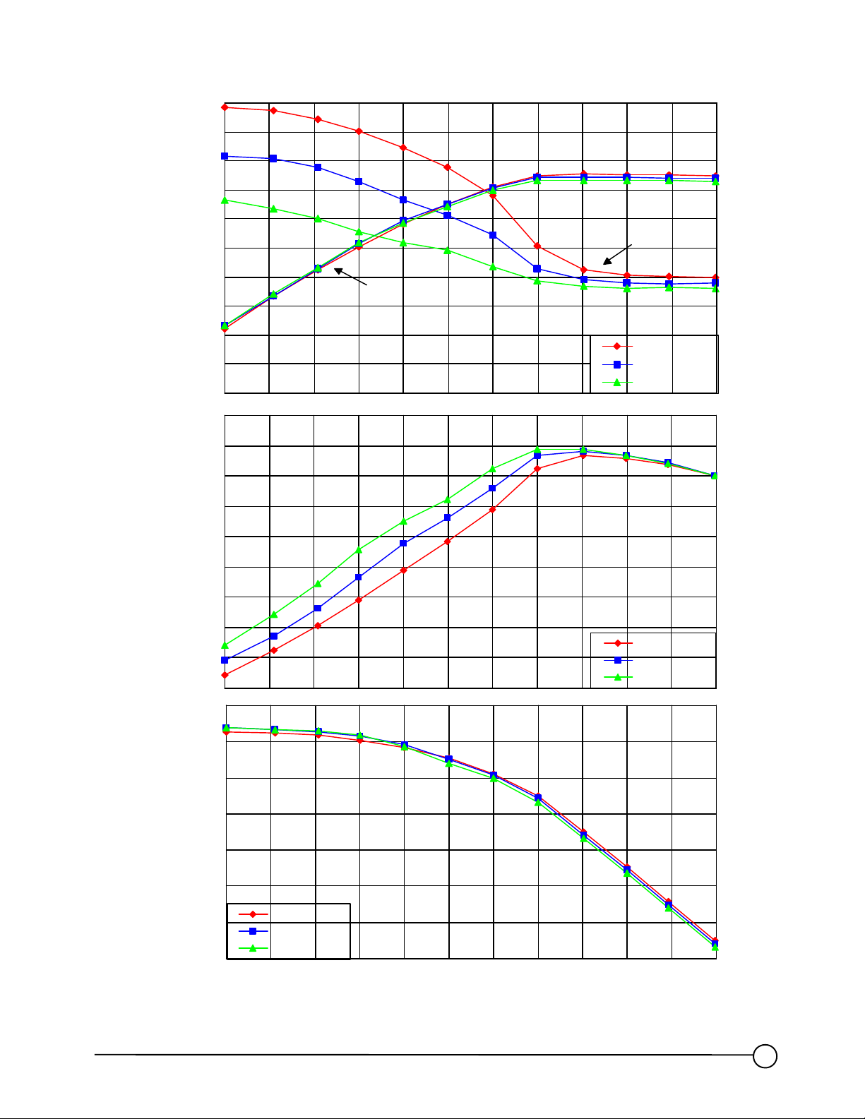
TGF4118-EPU RF Performance for Vd = 8.0 V, F = 2.3 GHz, and TA = 25°C
Quiescent Id is 1.69 A (Vg = -1.1 V), 1.38 A (Vg = -1.3 V), and 1.06 A (Vg = -1.5 V)
140
42
130
120
110
100
90
80
Pout
70
60
Predicted Channel Temp (°C)
50
40
60
55
50
45
40
Tch
Vg = -1.1 V
Vg = -1.3 V
Vg = -1.5 V
41
40
39
38
37
36
35
Output Power (dBm)
34
33
32
35
30
25
Power Added Efficiency %
20
15
15
14
13
12
11
Gain (dB)
10
9
8
20 21 22 23 24 25 26 27 28 29 30 31
Vg = -1.1 V
Vg = -1.3 V
Vg = -1.5 V
Input Power (dBm)
Vg = -1.1 V
Vg = -1.3 V
Vg = -1.5 V
TriQuint Semiconductor Texas Phone: 972 994-8465 Fax 972 994-8504 Web: www.triquint.com
3
Page 4

TGF4118-EPU RF Performance for Vd = 9.0 V, F = 2.3 GHz, and TA = 25°C
Quiescent Id is 1.66 A (Vg = -1.1 V), 1.39 A (Vg = -1.3 V), and 1.09 A (Vg = -1.5 V)
160
42
150
140
130
120
110
100
90
Pout
80
Predicted Channel Temp (°C)
70
60
55
50
45
40
35
Tch
Vg = -1.1 V
Vg = -1.3 V
Vg = -1.5 V
41
40
39
38
37
36
35
Output Power (dBm)
34
33
32
30
25
20
Power Added Efficiency %
15
10
15
14
13
12
11
Gain (dB)
10
9
8
20 21 22 23 24 25 26 27 28 29 30 31
Vg = -1.1 V
Vg = -1.3 V
Vg = -1.5 V
Input Power (dBm)
Vg = -1.1 V
Vg = -1.3 V
Vg = -1.5 V
TriQuint Semiconductor Texas Phone: 972 994-8465 Fax 972 994-8504 Web: www.triquint.com
4
Page 5

DC Characteristics for the TGF4118-EPU
DC probe Parameters Nominal Unit
IDSS Drain Saturation Current 4410 mA
GM Transconductance 2970 mS
VP Pinch Off Voltage -1.85 V
BVGS Breakdown Voltage Gate-Source -22 V
BVGD Breakdown Voltage Gate-Drain -22 V
Example of DC I-V Curves
Vg = 0.0 V to -2.75 V in 0.25 steps TA = 25°C
4500
4000
3500
3000
2500
2000
1500
Drain Current (mA)
1000
500
0
0 1 2 3 4 5 6 7 8 9
Drain Voltage (V)
Absolute Maximum Ratings
Drain-to-source Voltage, Vds..............................…………………………………………..........12 V
Gate-to-source Voltage, Vgs..................………………………………………….............-5 V to 0 V
Mounting Temperature.................……………………………………….….........………………320°C
Storage Temperature.....................…………………………………….….............… -65°C to 200°C
Power Dissipation...........…………….………………………………………..refer to Thermal Model
Operating Channel Temperature………………………………………….….refer to Thermal Model
Stresses beyond those listed under absolute maximum ratings may cause permanent damage to the device.
These are stress ratings only, and functional operation of the device at these or any other conditions beyond
those indicated in this document is not implied. Exposure to absolute maximum rated conditions for extended
periods of time may affect device reliability.
TriQuint Semiconductor Texas Phone: 972 994-8465 Fax 972 994-8504 Web: www.triquint.com
5
Page 6

TGF4118-EPU Linear Model
Vds = 7 V and Ids = 1.24 A at T = 25°C
FET Elements
Lg = .00176 nH
Rg = 0.42115 Ω
Rgs = 5447 Ω
Ri = .05082 Ω
Cgs = 18.82602 pF
Cdg = 1.03674 pF
Rdg = 13600 Ω
Rs = 0.06265 Ω
Ls = 0.00869 nH
Rds = 6.40925 Ω
Cds = 3.72019 pF
Rd = 0.01831 Ω
Ld = 0.00195 nH
VCCS Parameters
M = 2.04398 S
A = 0
R1 = 1E19
R2 = 1E19
F = 0
T = 4.5116 pS
Lg Rg
G
Ri
Rgs
Cgs
Cdg
Rdg
VCCS
R1 R2 Rds
Rs
Ls
Rd Ld
D
Cds
Freq-GHz MAG-S11 ANG-S11 MAG-S21 ANG-S21 MAG-S12 ANG-S12 MAG-S22 ANG-S22
0.5 0.96061 -157.13 4.44294 98.2855 0.00932 14.7392 0.85196 -178.271
1 0.96275 -168.492 2.25188 88.8751 0.00949 13.5187 0.85594 -178.561
1.5 0.96332 -172.363 1.49968 83.3713 0.00955 15.8589 0.85818 -178.438
2 0.9637 -174.323 1.11963 78.9074 0.00962 19.1829 0.86065 -178.22
2.5 0.96407 -175.515 0.88979 74.9064 0.00971 22.9596 0.86355 -177.98
3 0.96446 -176.325 0.73541 71.1835 0.00985 26.9945 0.86689 -177.746
3.5 0.96488 -176.917 0.62432 67.6655 0.01003 31.1758 0.8706 -177.53
4 0.96532 -177.374 0.54038 64.3208 0.01028 35.4143 0.87462 -177.338
4.5 0.96579 -177.743 0.47464 61.1349 0.01058 39.6273 0.87887 -177.174
5 0.96628 -178.05 0.42171 58.1017 0.01096 43.7382 0.88328 -177.04
TriQuint Semiconductor Texas Phone: 972 994-8465 Fax 972 994-8504 Web: www.triquint.com
6
Page 7

Thermal Model of TGF4118-EPU
Predicted Channel Temperature vs Base Plate Temperature
With a .020" CM15 (15/85 Copper Molybdenum) carrier plate solder attached
250
240
230
220
210
200
190
180
170
160
150
140
130
120
110
100
Channel Temperature (°C)
90
80
70
60
50
25 35 45 55 65 75 85 95 105 115 125
using 0.0015" AuSn (80/20) solder
Pd = 5 Watts
Pd = 10 Watts
Base Plate Temperature (°C)
Tc = 2.052 + 6.796 x Pd + 0.1465 x Pd 2 + (1.002 + 0.01999 x Pd + 0.0002725 x Pd 2) x Tbase
(Predicted Channel Temperature equation for the given assembly stack up)
This model assumes perfect solder connections (no voids) between the FET and the carrier plate.
HFETChannel Temperature vs Median Life
350
300
250
200
Channel Temperature (°C)
150
100
0 1 2 3 4 5 6 7 8 9 10
Median Life (10^X Hours)
TriQuint Semiconductor Texas Phone: 972 994-8465 Fax 972 994-8504 Web: www.triquint.com
7
Page 8

Mechanical Drawing of TGF4118-EPU
(0.305)
81.0
(2.057)
76.3
(1.938)
69.0
65.3
(1.659)
48.8
(1.239)
(1.753)
61.6
(1.565)
52.5
(1.333)
45.1
(1.145)
Gate
Alternate gate pad
35.9
32.2
(0.819)
15.7
(0.399)
4.7
(0.119)
0.0
0.0
7.4
(0.187)
24.9
(0.632)
36.0
(0.914)
(0.913)
28.5
(0.725)
19.4
(0.493)
12.0
Units: mils (mm)
Thickness: 4.0 (0.10)
Gate pad sizes are 4.0 x 4.0 (0.10 x 0.10)
Drain pad sizes are 4.7 x 14.5 (0.12 x 0.37)
A minimum of four gate bonds and eight drain
bonds is recommended for operation. Sources are
connected to backside metalization. Alternate gate
and drain pads are located on either end of the
FET for paralleling TGF4118-EPUs.
Drain
Alternate drain pad
TriQuint Semiconductor Texas Phone: 972 994-8465 Fax 972 994-8504 Web: www.triquint.com
8
Page 9

Application circuit for the TGF4118-EPU at 2.3 GHz
The FET is soldered using AuSn solder at 300 C for 30 secs. Input and Output matching networks are
0.381 mm ZrSn Tioxide substrates (Er = 38). The design load impedance is between 4 Ω and 5 Ω with
the 6 pF output capacitance of the FETincluded in the output network. For further explanation refer to
the application note “Designing High Efficiency Amplifiers using HFETs”. The carrier plate is 0.51 mm
gold plated copper molybdenum. Gold wire (0.018 mm) is used for the bonds. Four gate bonds are
required with a length of 0.42 mm. Eight drain bonds are required with a length of 0.42 mm. Bondwire
end points on the FET are in the middle of the bond pads. Refer to the figures above for bondwire
locations. Connection between the 50 ohm line input to the input match is made by a parallel RC
network. R1 in this network is 10 ohms, and C1 is 5.6 pF. The components used are surface mount
0603 piece parts.
TriQuint Semiconductor Texas Phone: 972 994-8465 Fax 972 994-8504 Web: www.triquint.com
9
 Loading...