

Page 1
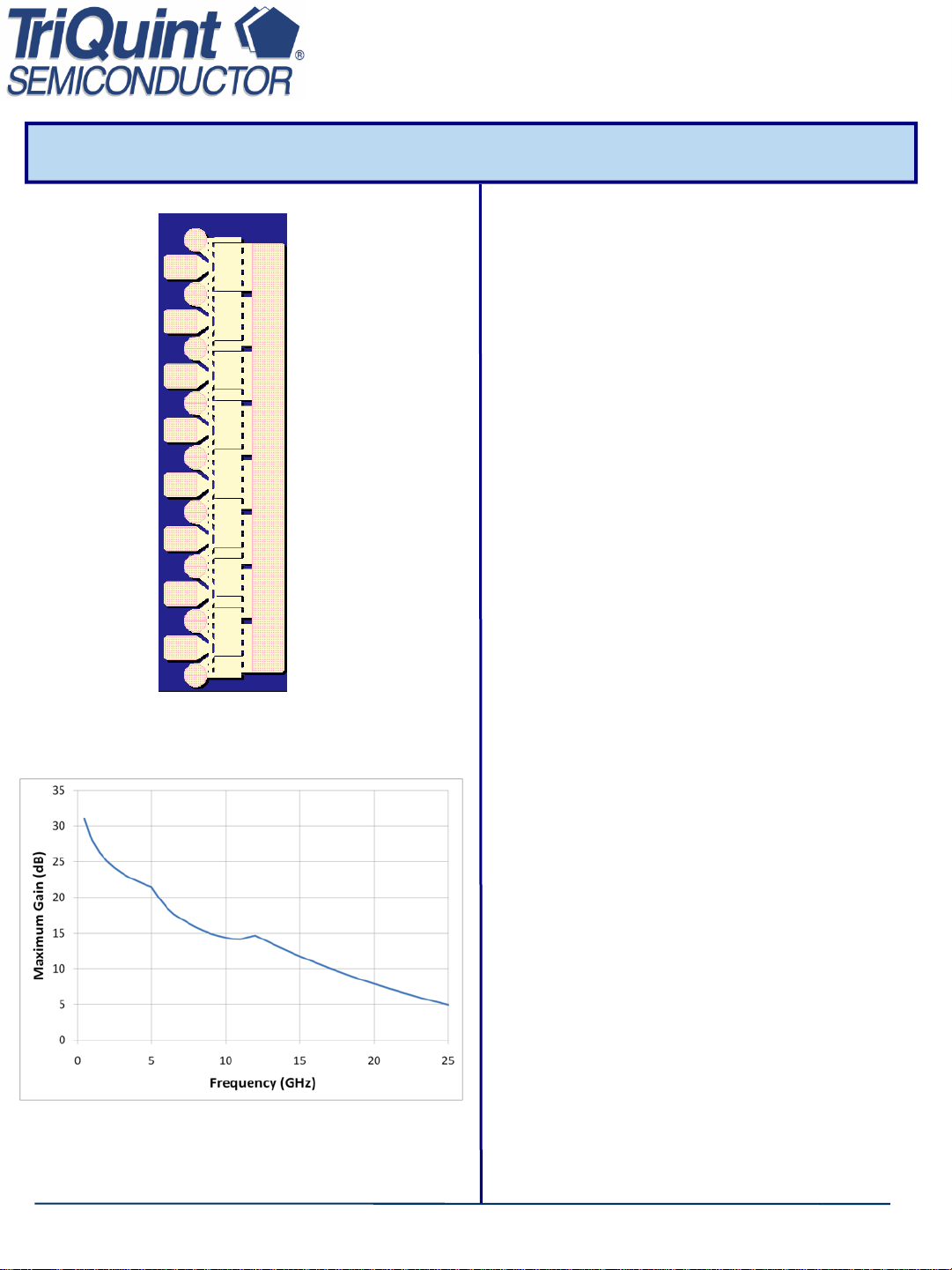
TGF2023-10
50 Watt Discrete Power GaN on SiC HEMT
Key Features
• Frequency Range: DC - 18 GHz
• 46.7 dBm Nominal Psat at 3 GHz
• 55% Maximum PAE
• 17.5 dB Nominal Power Gain
• Bias: Vd = 28 - 32 V, Idq = 1 A, Vg = -3.6 V Typical
• Technology: 0.25 um Power GaN on SiC
• Chip Dimensions: 0.82 x 2.48 x 0.10 mm
Primary Applications
• Defense & Aerospace
• Broadband Wireless
Bias conditions: Vd = 28 V, Idq = 1 A, Vg = -3.6 V Typical
TriQuint Semiconductor: www. triquint.com (972)994-8465 Fax (972)994-8504 [email protected]
Product Description
The TriQuint TGF2023-10 is a discrete 10 mm
GaN on SiC HEMT which operates from DC-18
GHz. The TGF2023-10 is designed using
TriQuint’s proven 0.25um GaN production process.
This process features advanced field plate
techniques to optimize microwave power and
efficiency at high drain bias operating conditions.
The TGF2023-10 typically provides 46.7 dBm of
saturated output power with power gain of 17.8 dB
at 3 GHz. The maximum power added efficiency
is 55% which makes the TGF2023-10 appropriate
for high efficiency applications.
Lead-free and RoHS compliant
.
Apr 2011 © Rev D
Datasheet subject to change without notice.
1
Page 2
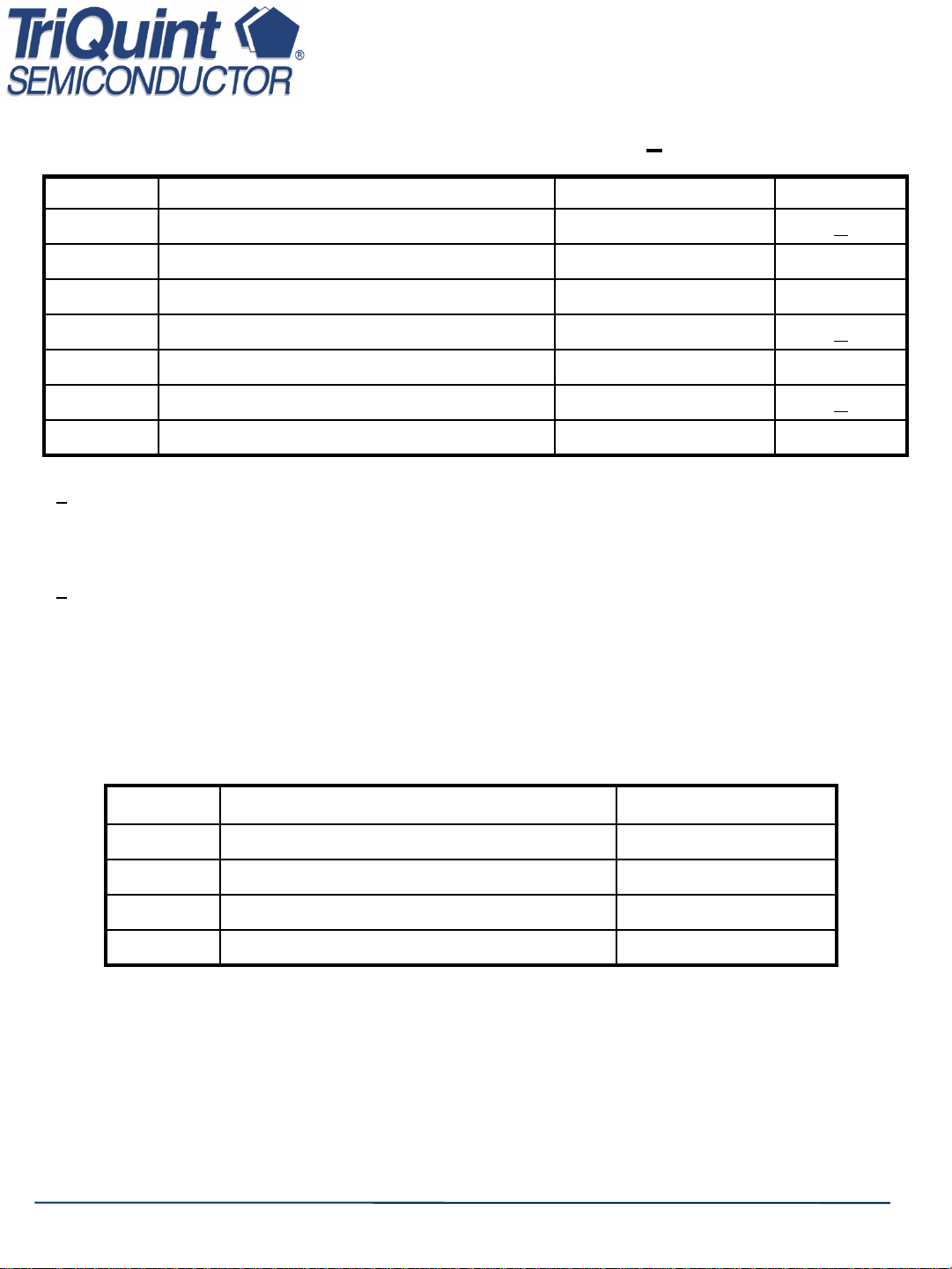
Table I
TGF2023-10
Absolute Maximum Ratings 1
/
Symbol Parameter V alue Notes
Vd Drain Voltage 40 V 2/
Vg Gate Voltage Range -50 to 0 V
Vdg Drain-Gate Voltage 80 V
Id Drain Current 10 A 2/
Ig Gate Current 56 mA
Pin Input Continuous Wave Power 40 dBm 2/
Tch Channel Temperature 200 °C
/ These ratings represent the maximum operable values for this device. Stresses beyond those listed
1
under “Absolute Maximum Ratings” may cause permanent damage to the device and / or affect
device lifetime. These are stress ratings only, and functional operation of the device at these
conditions is not implied.
/ Combinations of supply voltage, supply current, input power, and output power shall not exceed the
2
maximum power dissipation listed in Table IV.
Table II
Recommended Operating Conditions
Symbol Parameter V alue
Vd Drain Voltage 28 - 32 V
Idq Drain Current 1 A
Id_Drive Drain Current under RF Drive 3 A
Vg Gate Voltage -3.6 V
TriQuint Semiconductor: www. triquint.com (972)994-8465 Fax (972)994-8504 [email protected]
Apr 2011 © Rev D
2
Page 3
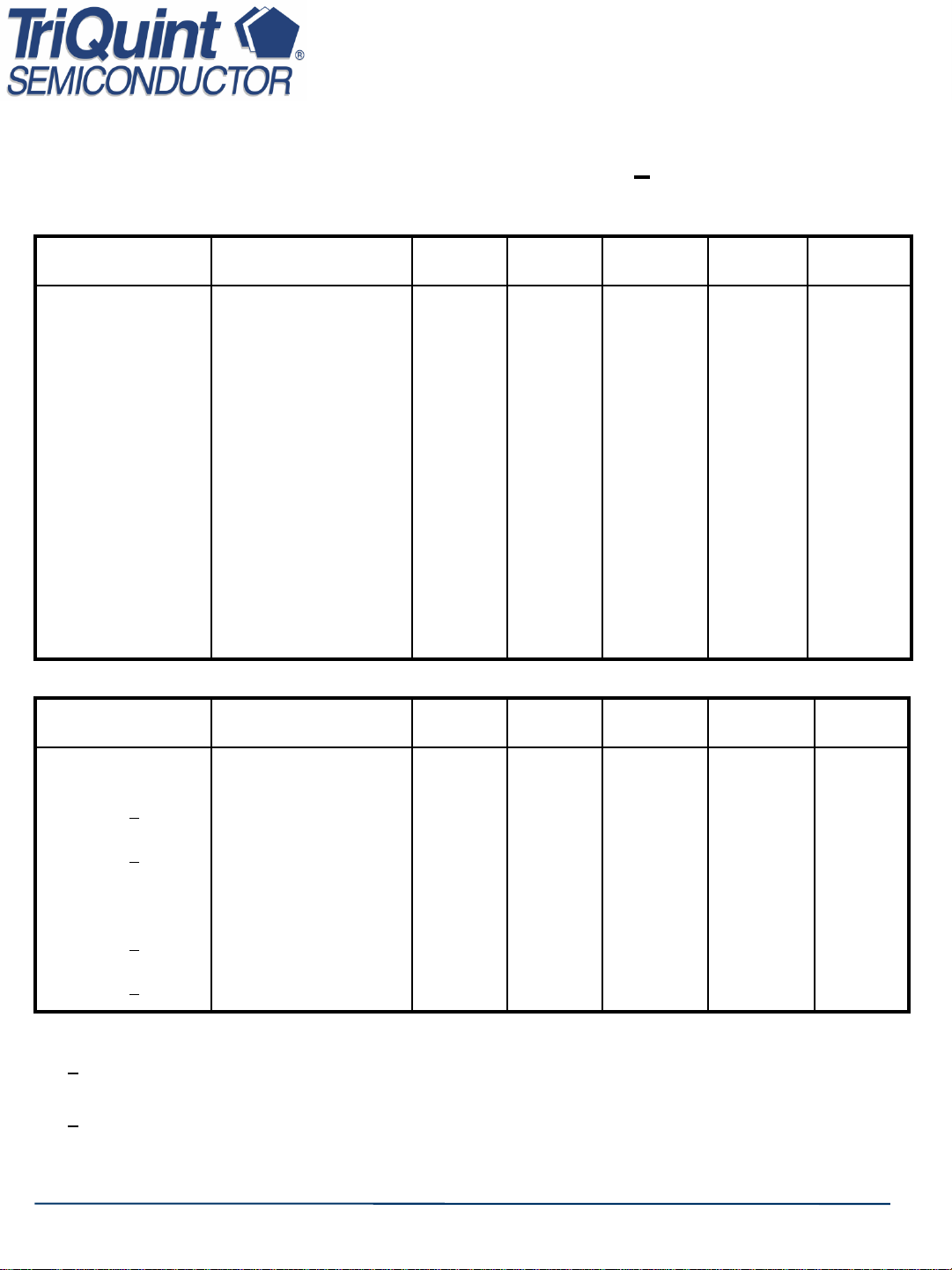
Table III
TGF2023-10
RF Characterization Table 1
/
Bias: Vd = 28 V, Idq = 1000 mA, Vg = -3.6V Typical
SYMBOL PARAMETER 3 GHz 6 GHz 10 GHz 14 GHz UNITS
Power Tuned:
Psat Saturated Output
Power
PAE Power Added
Efficiency
Gain Power Gain 17.5 11.5 8.9 5.6 dB
Efficiency Tuned:
Psat Saturated Output
Power
PAE Power Added
Efficiency
Gain Power Gain 16.8 12.1 9.2 5.5 dB
46.7 46.0 45.8 44.3 dBm
55 53 47 38 %
45.4 44.3 45.5 44.3 dBm
60 60 49 39 %
SYMBOL PARAMETER 3 GHz 6 GHz 10 GHz 14 GHz UNITS
Power Tuned:
/ Parallel Resistance 79.3 81.9 61.5 49.9 Ω·mm
Rp 2
Cp 2
/ Parallel Capacitance 0.524 0.348 0.426 0.432 pF/mm
Efficiency Tuned:
Rp 2
/ Parallel Resistance 153 171 72.1 53.1 Ω·mm
/ Parallel Capacitance 0.426 0.372 0.414 0.472 pF/mm
Cp 2
1/ Values in this table are engineering estimates scaled from measurements on the 1.25 mm
GaN/SiC unit cell (see TGF2023-01 datasheet)
2
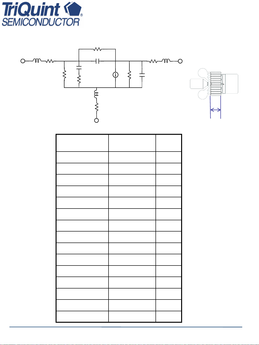
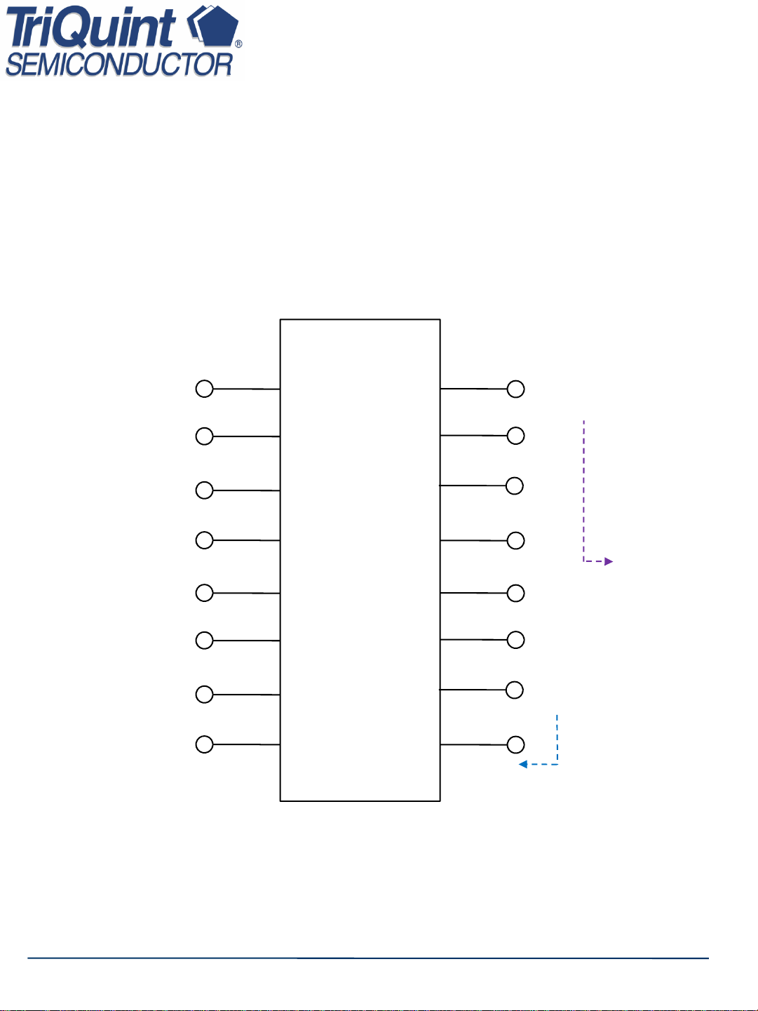
/ Large signal equivalent output network (normalized) (see figure, pg 7)
TriQuint Semiconductor: www. triquint.com (972)994-8465 Fax (972)994-8504 [email protected]
Apr 2011 © Rev D
3
Page 4
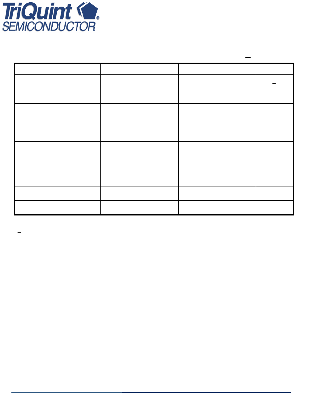
Table IV
TGF2023-10
Power Dissipation and Thermal Properties 1
Parameter Test Conditions V alue Notes
Maximum Power Dissipation Tbaseplate = 70 ºC Pd = 64 W
Tchannel = 200 ºC
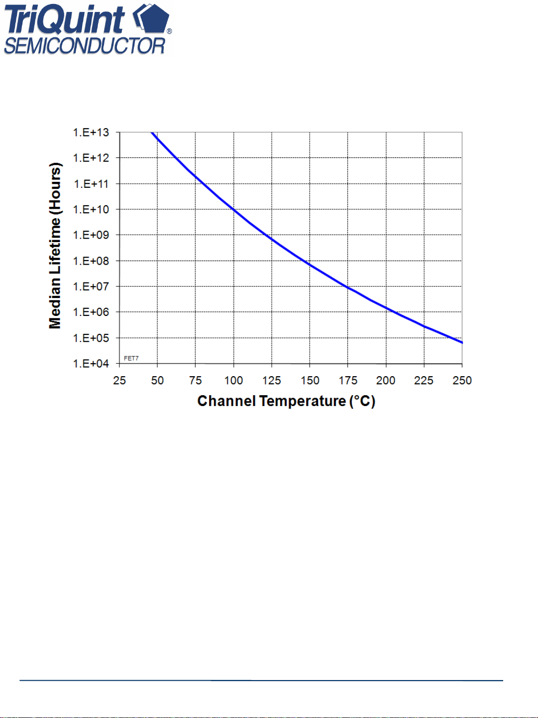
Tm = 1.5E+6 Hrs
Thermal Resistance, θjc Vd = 28 V
Id = 1 A
Pd = 28 W
Tbaseplate = 70 ºC
Thermal Resistance, θjc
Under RF Drive
Mounting Temperature 30 Seconds 320 ºC
Storage Temperature -65 to 150 ºC
Vd = 28 V
Id = 2.98 A
Pout = 46.7 dBm
Pd = 37.6 W
Tbaseplate = 70 ºC
θjc = 2.0 (ºC/W)
Tchannel = 126 ºC
Tm = 6.4E+8 Hrs
θjc = 2.0 (ºC/W)
Tchannel = 145 ºC
Tm = 1.1E+8 Hrs
/
2/
1
/ Assumes eutectic attach using 1mil thick 80/20 AuSn mounted to a 10mil CuMo Carrier Plate
2
/ Channel operating temperature will directly affect the device median lifetime. For maximum life, it is
recommended that channel temperatures be maintained at the lowest possible levels.
TriQuint Semiconductor: www. triquint.com (972)994-8465 Fax (972)994-8504 [email protected]
Apr 2011 © Rev D
4
Page 5
TGF2023-10
Median Lifetime vs Channel Temperature
TriQuint Semiconductor: www. triquint.com (972)994-8465 Fax (972)994-8504 [email protected]
Apr 2011 © Rev D
5
Page 6
Gate
Linear Model for 1.25 mm Unit GaN Cell (UGC)
Rdg
Lg Rg Cdg Rd Ld
Drain
Cgs
Rgs
+
v
i
-
R
i
gm v
Ls
Rs
Rds Cds
i
TGF2023-10
Source
MODEL
PARAMETER
Rg
Rs
Rd
gm
Cgs
Ri
Cds
Rds
Cgd
Tau
Vd=28V
Idq=125mA
0.78
0.13
1.28
0.270
1.79
0.26
0.308
123.6
0.064
2.78
Unit GaN cell (UGC)
Reference Plane
UNITS
Ω
Ω
Ω
S
pF
Ω
pF
Ω
pF
pS
Ls
Lg
Ld
Rgs
Rgd
TriQuint Semiconductor: www. triquint.com (972)994-8465 Fax (972)994-8504 [email protected]
0.0058
-0.013
0.018
8900
1730000
Apr 2011 © Rev D
nH
nH
nH
Ω
Ω
6
Page 7
TGF2023-10
Complete 10mm GaN HEMT Linear Model
Includes 8 UGC, 9 vias, and 16 bonding pads
Gate Pads
1
3
5
7
9
11
13
15
.s16p file
Drain Pads
2
Γ_load
4
6
8
10
12
14
16
Rp, Cp
TriQuint Semiconductor: www. triquint.com (972)994-8465 Fax (972)994-8504 [email protected]
Apr 2011 © Rev D
7
Page 8
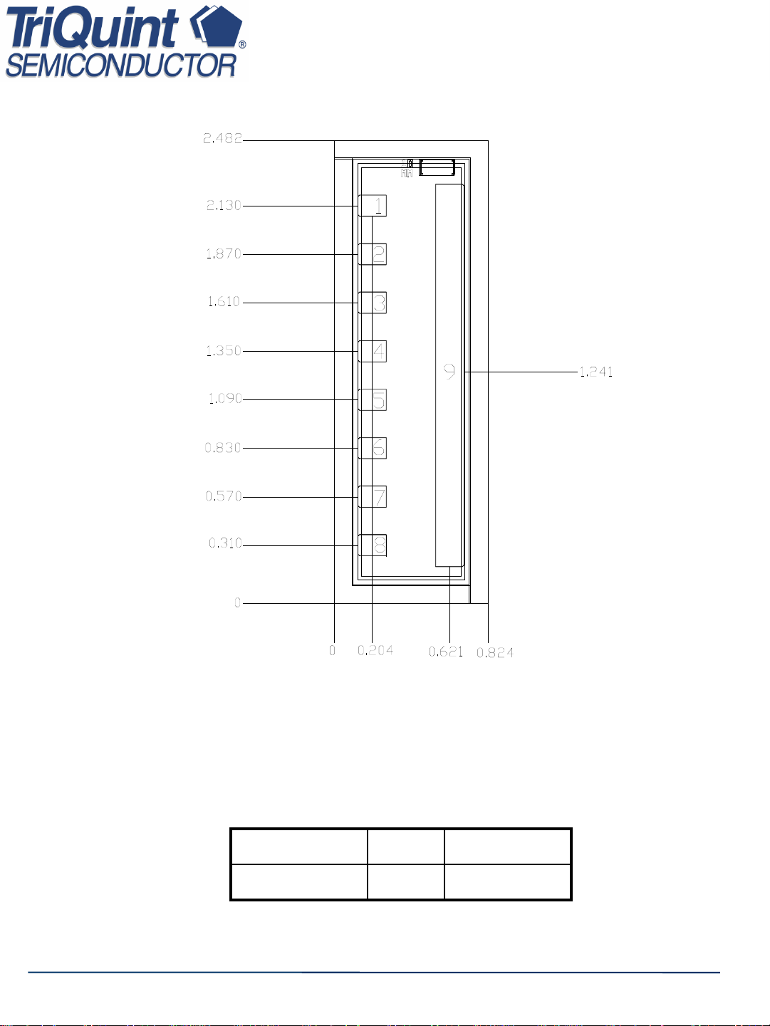
Mechanical Drawing
TGF2023-10
Units: millimeters
Thickness: 0.100
Die x,y size tolerance: +/- 0.050
Chip edge to bond pad dimensions are shown to center of pad
Ground is backside of die
Bond Pad #1 - 8 Vg 0.154 x 0.115
Bond Pad #9 Vd 0.154 x 2.050
GaAs MMIC devices are susceptible to damage from Electrostatic Discharge. Proper precautions should
be observed during handling, assembly and test.
TriQuint Semiconductor: www. triquint.com (972)994-8465 Fax (972)994-8504 [email protected]
Apr 2011 © Rev D
8
Page 9
TGF2023-10
Assembly Notes
Component placement and adhesive attachment assembly notes:
• Vacuum pencils and/or vacuum collets are the preferred method of pick up.
• Air bridges must be avoided during placement.
• The force impact is critical during auto placement.
• Organic attachment (i.e. epoxy) can be used in low-power applications.
• Curing should be done in a convection oven; proper exhaust is a safety concern.
Reflow process assembly notes:
• Use AuSn (80/20) solder and limit exposure to temperatures above 300°C to 3-4 minutes, maximum.
• An alloy station or conveyor furnace with reducing atmosphere should be used.
• Do not use any kind of flux.
• Coefficient of thermal expansion matching is critical for long-term reliability.
• Devices must be stored in a dry nitrogen atmosphere.
Interconnect process assembly notes:
• Ball bonding is the preferred interconnect technique, except where noted on the assembly diagram.
• Force, time, and ultrasonics are critical bonding parameters.
• Aluminum wire should not be used.
• Devices with small pad sizes should be bonded with 0.0007-inch wire.
Ordering Information
Part ECCN Package Style
TGF2023-10 3A001.b.3.b GaN on SiC Die
GaAs MMIC devices are susceptible to damage from Electrostatic Discharge. Proper precautions should
be observed during handling, assembly and test.
TriQuint Semiconductor: www. triquint.com (972)994-8465 Fax (972)994-8504 [email protected]
Apr 2011 © Rev D
9
 Loading...