

Page 1
Product Data Sheet
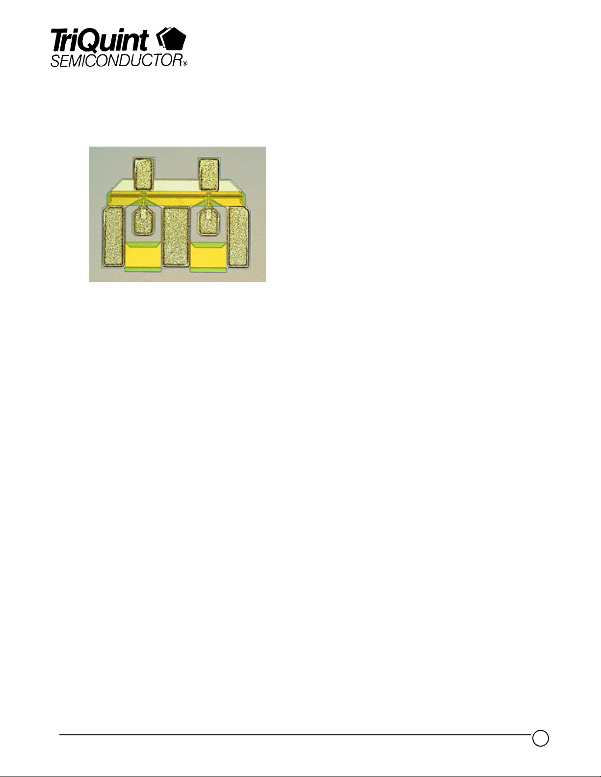
Discrete MESFET TGF1350-SCC
Key Features and Performance
• 0.5 um x 300 um FET
• 1.5 dB Noise Figure with 11dB
Associated Gain at 10 GHz
• 2.5 dB Noise Figure with 7 dB
Associated Gain at 18 GHz
• All-gold Metallization for High Reliability
• Recessed Gate Structure
Description
The TriQuint TGF1350-SCC is a single-gate GaAs field-effect transistor (FET) used
for low-noise applications DC to 18 GHz. Bond pad is gold plated for compatibility
with thermocompression and thermosonic compatibility wire-bonding processes.
The TGF1350-SCC is readily assembled using automated equipment. Die attach
should be accomplished with conductive epoxy only. Eutectic attach is not
recommended .
TriQuint Semiconductor Texas : (972)994 8465 Fax: (972)994 8504 Web: www.triquint.com
1
Page 2
Product Data Sheet
TGF1350-SCC
TriQuint Semiconductor Texas : (972)994 8465 Fax: (972)994 8504 Web: www.triquint.com
2
Page 3

Product Data Sheet
TGF1350-SCC
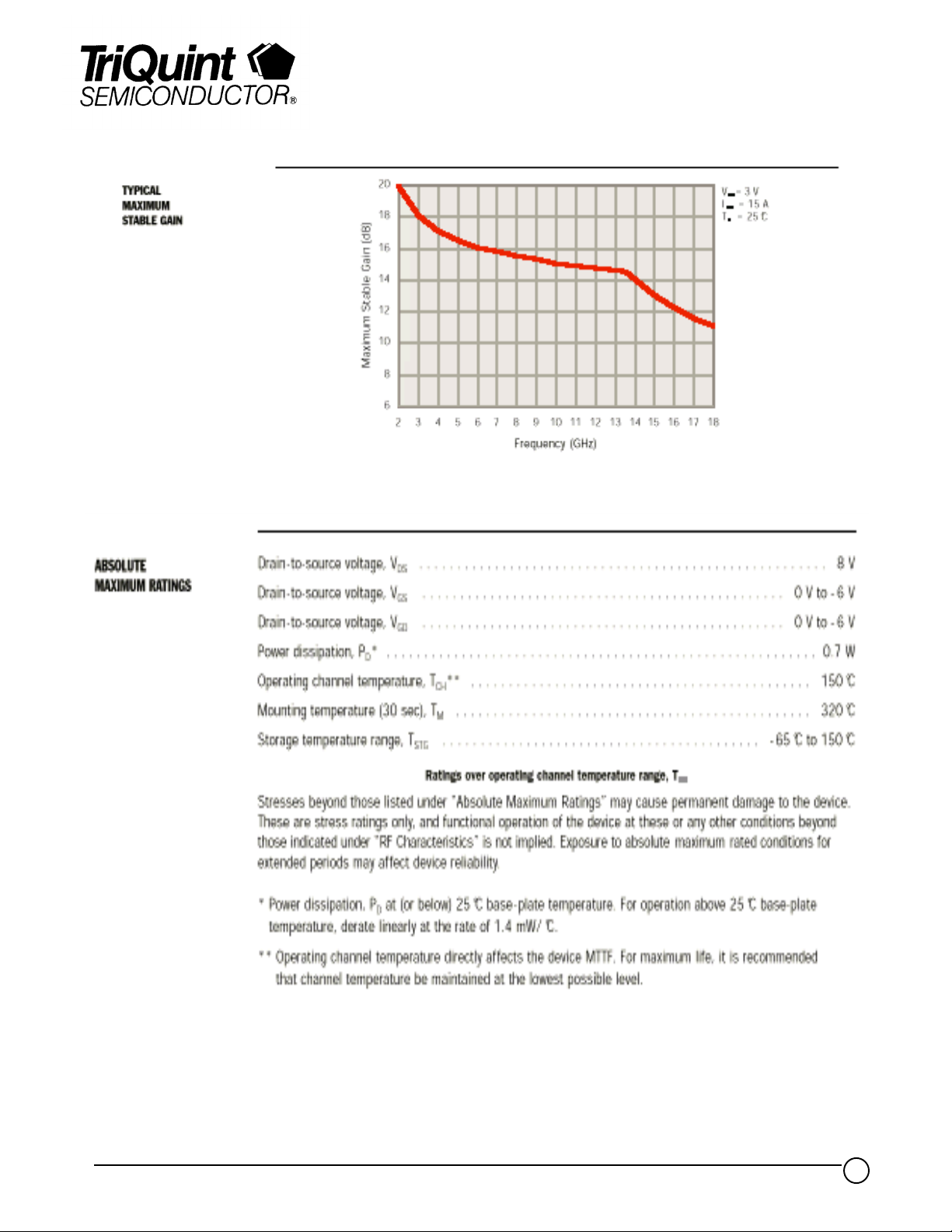
TYPICAL S-PARAMETERS
Frequency
S
(G Hz ) MAG ANG ( °) MAG ANG (°) MAG ANG (°) MAG ANG (°)
11
S
21
S
12
S
22
2.0 0.98 - 28 3.22 157 0.03 75 0.71 - 12
2.5 0.96 - 36 3.17 151 0.04 71 0.71 - 14
3.0 0.93 - 44 3.07 146 0.04 68 0.71 - 14
3.5 0.93 - 51 2.99 141 0.05 65 0.69 - 16
4.0 0.90 - 56 2.88 137 0.05 62 0.68 - 17
4.5 0.89 - 60 2.78 133 0.05 61 0.68 - 19
5.0 0.88 - 64 2.73 129 0.06 60 0.67 - 24
5.5 0.87 - 67 2.65 125 0.06 58 0.66 - 28
6.0 0.85 - 70 2.55 121 0.06 56 0.66 - 30
6.5 0.83 - 74 2.46 118 0.06 55 0.66 - 31
7.0 0.82 - 77 2.36 116 0.06 54 0.66 - 32
7.5 0.82 - 80 2.28 113 0.06 54 0.66 - 32
8.0 0.81 - 82 2.22 110 0.06 53 0.66 - 33
8.5 0.81 - 85 2.15 107 0.06 52 0.65 - 34
9.0 0.80 - 88 2.12 104 0.06 51 0.65 - 38
9.5 0.79 - 92 2.08 101 0.06 51 0.65 - 40
10.0 0.78 - 96 2.05 98 0.06 51 0.65 - 43
10.5 0.78 - 99 2.02 95 0.06 50 0.65 - 45
11.0 0.77 - 103 2.00 92 0.06 48 0.65 - 48
11.5 0.78 - 106 1.96 88 0.06 46 0.65 - 51
12.0 0.77 - 110 1.90 84 0.06 44 0.65 - 54
12.5 0.77 - 114 1.84 81 0.06 42 0.64 - 56
13.0 0.76 - 117 1.79 79 0.06 39 0.64 - 58
13.5 0.75 - 120 1.74 76 0.06 37 0.64 - 60
14.0 0.75 - 123 1.69 73 0.07 35 0.64 - 64
14.5 0.74 - 125 1.64 69 0.07 32 0.64 - 69
15.0 0.74 - 128 1.56 65 0.07 29 0.65 - 74
15.5 0.74 - 131 1.49 61 0.07 25 0.66 - 78
16.0 0.73 - 133 1.43 59 0.08 23 0.65 - 81
16.5 0.72 - 136 1.38 57 0.08 21 0.65 - 81
17.0 0.73 - 139 1.36 54 0.08 21 0.66 - 81
17.5 0.73 - 140 1.31 52 0.09 22 0.66 - 82
18.0 0.74 - 142 1.26 50 0.09 22 0.66 - 83
T
= 25oC, VDS = 3 V, IDS = 15mA
A
Reference planes for S-parameter data are located at center of gate and drain bond
pads. Three 0.7 mil diameter wires, approximately 13 mils long, are bonded from the
center of each of the source pads to ground. The S-parameters are also available on
floppy disk and the world wide web.
TriQuint Semiconductor Texas : (972)994 8465 Fax: (972)994 8504 Web: www.triquint.com
3
Page 4

Product Data Sheet
G
V
V
TGF1350-SCC
RF CHARACTERISTICS
DC CHARACTERISTICS
V
(BR)GDO
V
(BR)GSO
V
GS(OFF)
I
DSS
G
M
P ARAMET ER TES T CO NDIT IONS TYP UNIT
NF
MIN
Minimu m no ise figure 10 GHz 1.5
A
Asso ciat ed gain 10 GHz 11
PARAMETER TEST CONDITIONS MIN TYP MAX UNIT
Gate–drain breakdown voltage I
Gate–s ource breakdown voltage I
Gate–source cutoff (pinch–off) V
volt ag e
Zero–gate–voltage drain current
at saturation
DC transconductance
*V
= VDS @ I
DSS
**VDS for I
DSS
is the drain voltage between 0.5V and 3.5V at which drain current is highest.
DSS
18 GHz 2.5 dB
18 GHz 7
= 3 V, IDS = 15mA, TA = 25OC
V
DS
= 1.0mA per mm - 6 V
GS
= 1.0mA per mm - 6 V
GD
= V
DS
I
= 0.5mA per mm
D
V
DS
V
GS
V
DS
GS
* - 0.5 - 1.2 - 3 V
DSS
= 0.5 V to 3.5V** 30 50 100 mA
= 0
= 0.5 V to V
= -0.25
TA = 25OC
DSS
*
40 50 78 mA
EQUIVALENT SCHEMATIC
TriQuint Semiconductor Texas : (972)994 8465 Fax: (972)994 8504 Web: www.triquint.com
4
Page 5

Product Data Sheet
TGF1350-SCC
TYPICAL MODEL
PARAMETERS
S TANDAR D
PARAMETER VALUE
Source resistance 5.62 0.6
r
s
Drain resistance 4.48 0.4
r
d
Gate resistance 4.68 0.5
r
g
Transconductance 52.32 6 mS
g
m
Drain–to–source resistance 224 40
r
ds
Input resistance 1.30 1
r
i
Gate–to–source capacitance 0.351 0.027 pF
C
gs
Gate–to–drain capacitance 0.0159 0.0037 pF
C
gd
Drain–to–source capacitance 0.0877 0.0095 pF
C
ds
Time constant 2.33 0.1 ps
τ
DE VIAT ION
UNIT
Ω
Ω
Ω
Ω
Ω
GaAs MMIC devices are susceptible to damage from Electrostatic Discharge. Proper precautions should be observed during
handing, assembly and test.
TriQuint Semiconductor Texas : (972)994 8465 Fax: (972)994 8504 Web: www.triquint.com
5
 Loading...