

Page 1
Product Data Sheet
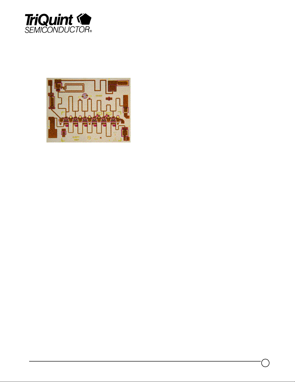
2 - 20 GHz Gain Block Amplifier TGA8622-SCC
Key Features and Performance
• 2 to 20 GHz Frequency Range
• 7.5 dB Gain with Greater than 30dB
Gain-Control Capability
• 20 dBm Output Power at 1 dB Gain
Compression
• 7 dB Noise Figure
• Input and Output SWR 1.7:1 Midband
• 2.769 x 2.159 x 0.152 mm (0.109 x
0.085 x 0.006 in.)
Description
The TriQuint TGA8622-SCC is a broadband general-purpose amplifier that operates
over the 2 to 20 GHz frequency range. Six 200um dual-gate FETs provide the
amplifier with a typical gain of 7.5 dB. Midband input and output SWRs are typically
1.7:1. This amplifier is directly cascadable and can be used in both gain control and
active temperature compensation applications. Ground is provided to the circuitry
through vias to the backside metallization.
The TGA8622-SCC is available in chip form and is readily assembled using
automated equipment. The device bond pads and backside are gold plated for
compatibility with eutectic alloy attach methods as well as thermocompression and
thermosonic wire-bonding processes.
TriQuint Semiconductor Texas Phone: (972)994 8465 Fax: (972)994 8504 Web: www.triquint.com
1
Page 2
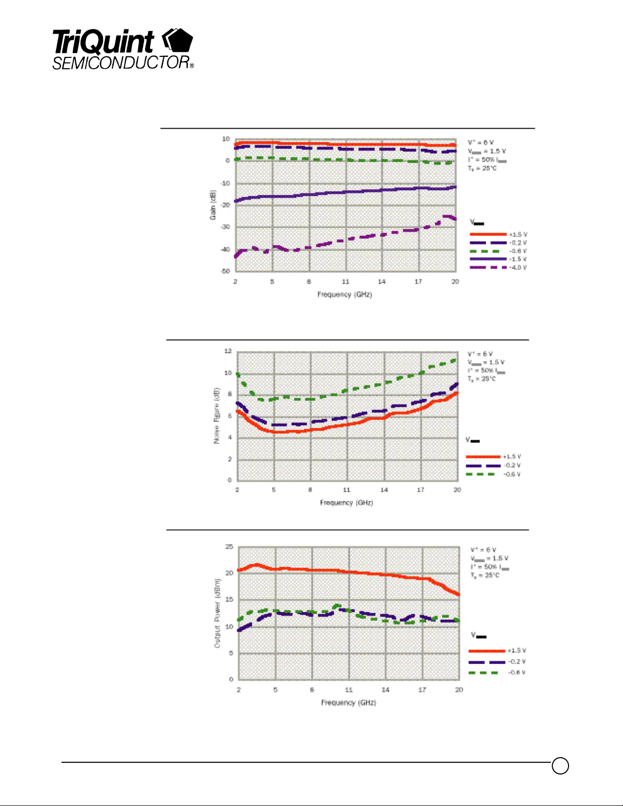
TYPICAL
SMALL-SIGNAL
POWER GAIN
Gp vs. V
CTRL
Product Data Sheet
TGA8622-SCC
V
for particular gain levels is shown for reference only and may vary from device to device.
CTRL
TYPICAL
NOISE FIGURE
NF vs. V
CTRL
TYPICAL
OUTPUT POWER
P
vs. V
1dB
CTRL
TriQuint Semiconductor Texas Phone: (972)994 8465 Fax: (972)994 8504 Web: www.triquint.com
2
Page 3
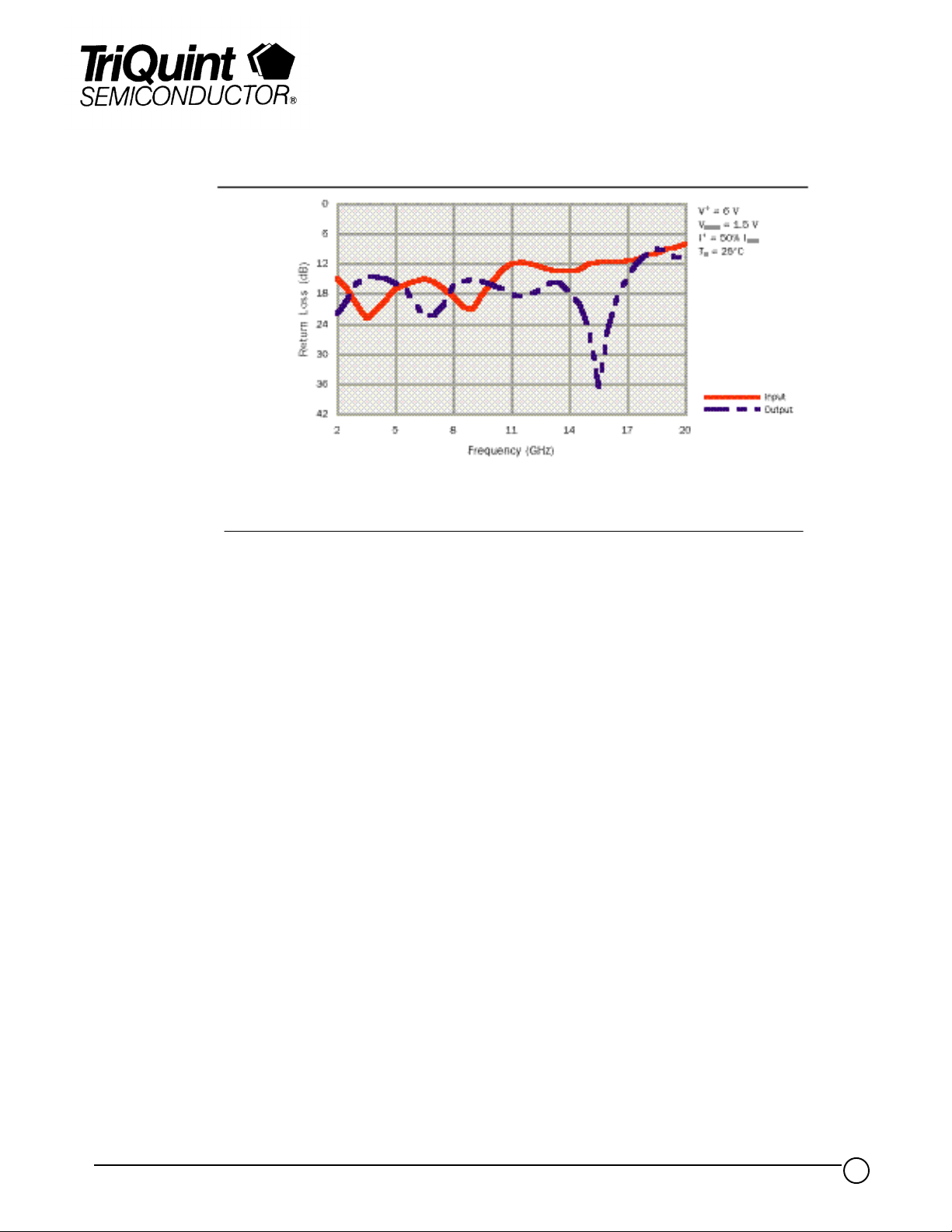
TYPICAL
…
…
.
.
…
/
RETURN LOSS
Product Data Sheet
TGA8622-SCC
ABSOLUTE
MAXIMUM
RATINGS
Positive supply voltage, V+………………………………………………………………………………….8 V
Positive supply voltage range w ith respect to negative supply voltage, V+ - V-……………………
0 V to 12 V
Negative supply voltage range, V-………………………………………………………………………… 0 V to -5 V
Gain control voltage range, V
Gain control voltage range w ith respect to positive supply voltage, V
Positive supply current, I+…..………………………………………………………………………………
Pow er dis sipation, P
, at (or below ) 25oC base-plate temperature *…………………………………
D
Operating Channel temperature, T
Mounting temperature (30 sec.), T
Storage temperature range, T
Ratings over oper ating channel temperature range, T
…………………………………………………………………………
CTRL
……………………………
CTR L
-5 V to 4 V
0 V to -10 V
370 mA
2.9 W
**………………………………………………………………………150oC
CH
…………………………………………………………………………320oC
M
……………………………………………………………………………-65 to 150oC
STG
(unless otherwise noted).
CH
Stresses beyond those listed under "A bsolute Maximum Ratings" may caus e per manent damage to the dev ice.
These are str ess ratings only, and functional operation of the device at these or any other conditions beyond
those indicated under "RF Charac teristics" is not implied. Exposur e to abs olute maximum rated conditions
for extended periods may af f ect device reliability.
* For operation abov e 25
o
C base-plate temperature, derate linearly at the rate of 6.1 mW
** Operating channel temperature ( T
) w ill d ir e c tly af f e c t t h e d e v ic e MTTF. Fo r ma x imum li f e, i t is r e c ommen d e d
CH
o
C.
that channel temperature be maintained at the low est possible level.
TriQuint Semiconductor Texas Phone: (972)994 8465 Fax: (972)994 8504 Web: www.triquint.com
3
Page 4

Product Data Sheet
TGA8622-SCC
TYPICAL S-PARAMETERS
Freque ncy S
(GHz) MAG ANG(°) MAG ANG(°) MAG ANG(°) MAG ANG(°) (dB)
11
S
21
S
12
S
22
2.0 0.18 168 2.34 128 0.007 81 0.08 55 7.4
2.5 0.14 150 2.55 108 0.011 59 0.15 -33 8.1
3.0 0.10 148 2.62 87 0.013 37 0.17 -81 8.4
3.5 0.07 175 2.66 66 0.014 16 0.19 -116 8.5
4.0 0.09 -160 2.64 46 0.014 -5 0.19 -143 8.4
4.5 0.12 -153 2.61 26 0.014 -24 0.18 -165 8.3
5.0 0.14 -158 2.57 7 0.014 -37 0.17 176 8.2
5.5 0.16 -166 2.54 -12 0.015 -61 0.14 160 8.1
6.0 0.17 -177 2.49 -30 0.015 -81 0.11 152 7.9
6.5 0.18 172 2.47 -48 0.016 -99 0.07 163 7.8
7.0 0.17 163 2.46 -66 0.016 -118 0.08 -166 7.8
7.5 0.14 159 2.46 -84 0.018 -136 0.11 -149 7.8
8.0 0.12 159 2.44 -103 0.020 -155 0.15 -149 7.8
8.5 0.09 166 2.43 -121 0.021 -172 0.17 -152 7.7
9.0 0.09 -174 2.42 -139 0.023 171 0.18 -153 7.7
9.5 0.12 -161 2.41 -158 0.024 155 0.17 -157 7.7
10.0 0.17 -157 2.40 -177 0.025 139 0.16 -160 7.6
10.5 0.22 -157 2.38 165 0.026 124 0.15 -165 7.5
11.0 0.26 -160 2.36 147 0.026 108 0.13 -167 7.4
11.5 0.27 -162 2.35 128 0.026 91 0.12 -167 7.4
12.0 0.26 -165 2.35 110 0.025 77 0.13 -167 7.4
12.5 0.24 -169 2.38 91 0.025 61 0.14 -172 7.5
13.0 0.23 -174 2.36 71 0.025 44 0.17 172 7.5
13.5 0.22 -178 2.35 53 0.025 25 0.17 144 7.4
14.0 0.21 -175 2.38 33 0.025 4 0.14 120 7.5
14.5 0.22 -169 2.38 12 0.027 -18 0.10 100 7.5
15.0 0.25 -164 2.38 -8 0.028 -41 0.06 80 7.5
15.5 0.26 -162 2.39 -29 0.030 -62 0.02 2 7.6
16.0 0.26 -162 2.36 -51 0.031 -84 0.07 -122 7.5
16.5 0.26 -166 2.31 -72 0.033 -104 0.13 -151 7.3
17.0 0.26 -170 2.33 -93 0.036 -125 0.19 -175 7.3
17.5 0.28 -172 2.31 -116 0.038 -146 0.25 159 7.3
18.0 0.33 -174 2.22 -138 0.035 -166 0.31 133 6.9
18.5 0.33 -174 2.19 -159 0.037 -174 0.36 114 6.8
19.0 0.36 -169 2.21 179 0.042 163 0.37 98 6.9
19.5 0.38 -167 2.29 155 0.041 140 0.29 95 7.2
20.0 0.40 -164 2.28 125 0.040 119 0.28 133 7.1
GAIN
= 25oC, V+ = 6 V, V
T
A
= 1.5 V, I+ = 50% I
CTRL
DSS
The reference planes for S-parameter data include bond wires as specified in the equivalent schematic.
The S-parameters are also available on floppy disk and the world wide web.
TriQuint Semiconductor Texas Phone: (972)994 8465 Fax: (972)994 8504 Web: www.triquint.com
4
Page 5

Product Data Sheet
I
TGA8622-SCC
RF CHARACTERISTICS
DC CHARACTERISTICS
P ARAMETER TEST C ONDITIONS TYP UNIT
G
P
Small-s ignal pow er gain f = 2 to 20 GHz 7.5 dB
SWR (in) Input s tanding w a ve ratio f = 2 to 10 GHz 1.3:1 -
f = 10 to 20 GHz 1.7:1
SWR (out) Output standing wa ve ratio f = 2 to 10 GHz 1.3:1 -
f = 10 to 20 GHz 1.7:1
P
1dB
Output power at 1–dB gain compres s ion f = 2 to 18 GHz 20 dBm
f = 18 to 20 GHz 17
NF Nois e figure f = 2 to 20 GHz 7 dB
f = 2 GHz 33
IP
3
Output third–order intercept point f = 10 GHz 33 dBm
f = 18 GHz 30
TA = 25oC, V+ = 6 V, V
P ARAMETER TEST CONDITIONS MIN MAX UNIT
Zero–gate–voltage drain current at saturation
DS S
= 1.5 V, I+ = 50% I
CTRL
V
= 0.5 V to 3.5 V, V
DS
DSS
GS
= 0 V
156 444 mA
TA = 25oC
V
for I
DS
is the drain voltage between 0.5 V and 3.5 V at which drain current is highest at DC Autoprobe.
DSS
EQUIVALENT
SCHEMATIC
TriQuint Semiconductor Texas Phone: (972)994 8465 Fax: (972)994 8504 Web: www.triquint.com
5
Page 6

RECOMMENDED
BIAS CIRCUIT
Product Data Sheet
TGA8622-SCC
6 V
RF connections: Bond using two 1.0-mil diameter, 20-mil-length gold bond wires at both RF Input and
RF Output.
Measuring I
Increase V+, V
: Set V-, V+, and V
DSS
from 0 V and measure I+ maximum for V+, V
CTRL
to 0 V. Connect V
CTRL
to V+. Short V- to ground.
CTRL
</= 4 V. I+ maximum is I
CTRL
DSS
.
Maximum gain bias (in this sequence):
Set V- to -1 V, V+ to 6 V, and V
to 1.5 V. Adjust V- to achieve I+ = 50% I
CTRL
Gain reduction: Set bias for maximum gain condition and decrease V
(I+ will drop accordingly; do not re-adjust V-.)
CTRL
.
DSS
from 1.5 V.
TriQuint Semiconductor Texas Phone: (972)994 8465 Fax: (972)994 8504 Web: www.triquint.com
6
Page 7

MECHANICAL
DRAWING
Product Data Sheet
TGA8622-SCC
GaAs MMIC devices are susceptible to damage from Electrostatic Discharge. Proper precautions should be observed
during handling, assembly and test.
TriQuint Semiconductor Texas Phone: (972)994 8465 Fax: (972)994 8504 Web: www.triquint.com
7
 Loading...