

Page 1

T R I Q U I N T S E M I C O N D U C T O R , I N C .
TGA8349-SCC Gain Block Amplifier
8349
DC to 14-GHz Frequency Range
●
1.2:1 Input SWR, 1.3:1 Output SWR
●
11-dB Small Signal Gain
●
16-dBm Output Power at 1 -dB Gain Compression at Midband
●
3.1-dB Noise Figure at Midband
●
3,4290 x 2,2860 x 0,101 mm (0.135 x 0.090 x 0.004 in.)
●
PHOTO ENLARGEMENT
DESCRIPTION
The TriQuint TGA8349 -SCC is a GaAs monolithic low -noise distributed amplifier designed
for use as a multi -octave general-purpose gain block. Nine 122 -µm gate width FETs provide 11-dB
nominal gain and 3.1- dB noise figure from DC to 14 -GHz. Typical power output is 16-dBm at
1-dB gain compression. Typical input SWR is 1.2:1 and output SWR is 1.3:1. Ground is provided to
the circuitry through vias to the backside metallization.The DC to 14 -GHz frequency range, dual - gate
AGC control and gain-flatness characteristics make the TGA8349 -SCC suitable for many system
applications including fiber optic.
The TGA8349-SCC is supplied in chip for m and is engineered for high -volume automated assembly.
All metal sur faces are gold plated to be compatible with ther mocompression and thermosonic
wire- bonding processes.
TriQuint Semiconductor, Inc. • Texas Facilities • (972) 995-8465
• www.triquint.com
Page 2
TGA8349-SCC
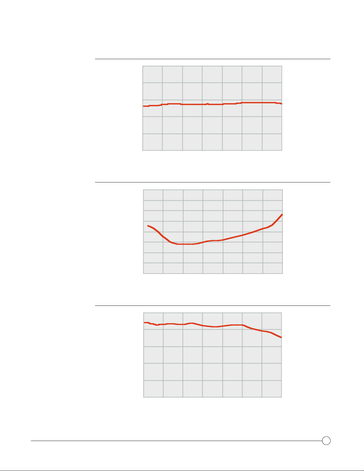
TYPICAL
SMALL SIGNAL
POWER GAIN
TYPICAL
NOISE FIGURE
20
16
12
8
Small-Signal Gain (dB)
4
0
02 46 8101214
Frequency (GHz)
8
7
6
5
4
V+= 8 V
V+= 8 V
V
= 1.5 V
= 1.5 V
V
CTR L
CTRL
+
+
= 80 mA
I
= 80 mA
I
T A= 25° C
= 25°C
T
A
V+= 8 V
V+= 8 V
V
= 1.5 V
CTR L
= 1.5 V
V
CTRL
+
+
= 80 mA
I
= 80 mA
I
T A= 25° C
= 25°C
T
A
TYPICAL
OUTPUT POWER
P
1dB
3
Noise Figure (dB)
2
1
0
02 46 8101214
Frequency (GHz)
20
16
12
8
Output Power (dBm)
4
0
0246 8101214
Frequency (GHz)
V+= 8 V
V+= 8 V
V
= 1.5 V
CTR L
= 1.5 V
V
CTRL
+
+
= 80 mA
I
= 80 mA
I
T A= 25° C
= 25°C
T
A
TriQuint Semiconductor, Inc. • Texas Facilities • (972) 995-8465
• www.triquint.com
2
Page 3
TGA8349-SCC
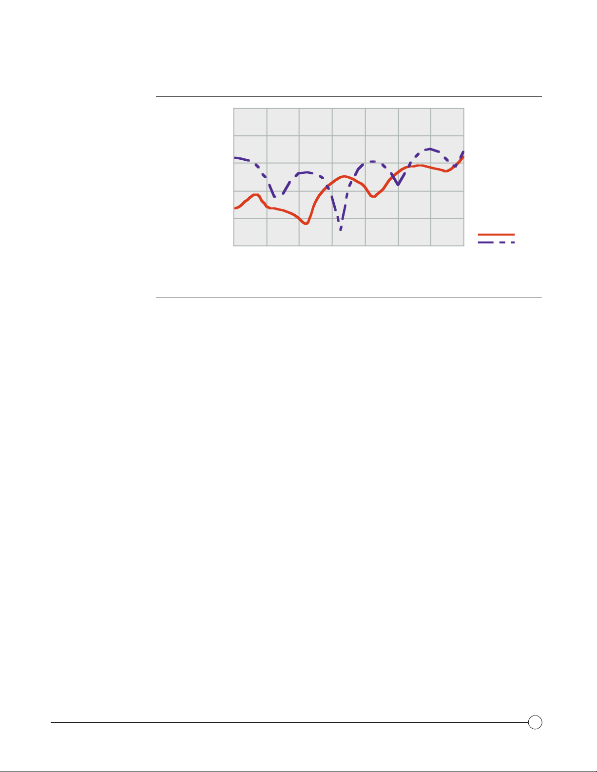
TYPICAL
RETURN LOSS
ABSOLUTE
MAXIMUM RATINGS
0
10
20
30
V+= 8 V
V+= 8 V
= 1.5 V
V
V
= 1.5 V
CTRL
CTR L
+
+
= 80 mA
I
= 80 mA
I
T A= 25° C
= 25°C
T
A
Return Loss (dB)
40
Input
Input
Output
50
0 2 4 6 8 10 12 14
Output
Frequency (GHz)
Positive supply voltage, V
Positive supply voltage range with respect to negative supply voltage, V+Positive supply voltage range with r espect to gain control voltage, V
+
.................................................................................................................. 13 V
V–.............................. 0 V to 13 V
-
V+.............................. 0 V to -13 V
CTRL
Negative supply voltage range, VG1............................................................................................-5 V to 0 V
Gain control voltage range, V
................................................................................................-5 V to 4 V
CTRL
Positive supply current, I+.............................................................................................................. 144 mA
Power dissipation, PD, at (or below) 25°C base-plate temperatur e* ...................................................... 2.6 W
Input continuous wave power, PIN.................................................................................................... 23 dBm
Operating channel temperature, TCH** ......................................................... ..................................... 150°C
Mounting temperature (30 sec), TM.................................................................................................. 320°C
Storage temperature range, T
Ratings over channel temperature range, TCH(unless otherwise noted)
............................................................................................-65 to 150°C
STG
Stresses beyond those listed under “Absolute Maximum Ratings” may cause permanent damage to the device.
These are stress ratings only, and functional operation of the device at these or any oth er conditions beyond
those indicated under “RF Characteristics” is not implied. Exposure to absolute maximum rated conditions for
extended periods may affect device reliability.
* For operation above 25°C base -plate temperature, derate linearly at the rate of 5.5 mW/5C.
** Operating channel temperature directly affects the device MTTF. For maximum life, it is r ecommended that
channel temperature be maintained at the lowest possible level.
TriQuint Semiconductor, Inc. • Texas Facilities • (972) 995-8465
• www.triquint.com
3
Page 4

TGA8349-SCC
TYPICAL S-PARAMETERS
Frequency S
(GHz) MAG ANG(°) MAG ANG(°) MAG ANG(°) MAG ANG(°) (dB)
11
S
21
S
12
S
22
0.1 0.02 115 3.32 173 0.001 85 0.12 180 10.4
0.5 0.02 92 3.34 155 0.003 73 0.12 161 10.5
1.0 0.02 26 3.36 130 0.005 53 0.11 142 10.5
1.5 0.03 -28 3.40 106 0.008 31 0.09 112 10.6
2.0 0.02 -72 3.46 80 0.011 6 0.05 80 10.8
2.5 0.02 -122 3.51 54 0.013 -20 0.02 21 10.9
3.0 0.01 -165 3.52 28 0.015 -46 0.03 -73 10.9
3.5 0.01 139 3.53 2 0.017 -71 0.05 -118 10.9
4.0 0.01 87 3.51 -24 0.019 -97 0.07 -151 10.9
4.5 0.01 12 3.48 -50 0.021 -121 0.07 -180 10.8
5.0 0.02 -74 3.48 -76 0.024 -146 0.06 155 10.8
5.5 0.03 -112 3.48 -101 0.026 -170 0.05 132 10.8
6.0 0.04 -142 3.49 -127 0.029 166 0.03 106 10.9
6.5 0.06 -167 3.52 -154 0.032 144 0.01 -123 10.9
7.0 0.05 167 3.51 180 0.035 120 0.04 -120 10.9
7.5 0.05 150 3.51 154 0.037 95 0.07 -139 10.9
8.0 0.04 141 3.51 127 0.039 71 0.10 -158 10.9
8.5 0.02 163 3.52 100 0.041 46 0.11 -177 10.9
9.0 0.03 -166 3.54 73 0.043 21 0.10 165 11.0
9.5 0.05 -162 3.58 46 0.045 -6 0.07 155 11.1
10.0 0.07 -167 3.63 18 0.047 -34 0.04 179 11.2
10.5 0.08 177 3.63 -11 0.049 -60 0.07 -142 11.2
11.0 0.09 167 3.68 -39 0.054 -89 0.12 -142 11.3
11.5 0.09 156 3.68 -69 0.057 -117 0.17 -160 11.3
12.0 0.08 149 3.68 -99 0.061 -144 0.18 -179 11.3
12.5 0.08 148 3.67 -129 0.066 -172 0.16 163 11.3
13.0 0.07 160 3.65 -160 0.069 160 0.11 156 11.3
13.5 0.09 174 3.63 168 0.072 131 0.09 -172 11.2
14.0 0.13 168 3.57 135 0.072 100 0.16 -156 11.0
14.5 0.16 151 3.46 101 0.072 68 0.23 -171 10.8
15.0 0.15 131 3.36 67 0.070 35 0.25 171 10.5
15.5 0.10 126 3.31 30 0.071 0 0.19 161 10.4
16.0 0.10 160 3.13 -10 0.069 -40 0.16 -171 9.9
V+= 8 V, V
= 1.5 V, I+= 80 mA, TA= 25°C
CTRL
Reference planes for S -parameter data include bond wir es as specified in the “Recommended Assembly
Diagram.”
GAIN
TriQuint Semiconductor, Inc. • Texas Facilities • (972) 995-8465
• www.triquint.com
4
Page 5

TGA8349-SCC
RF CHARACTERISTICS
DC CHARACTERISTICS
PARAMETER TEST CONDITIONS TYP UNIT
G
P
Small–signal power gain f = DC to 14 GHz 11 dB
SWR(in) Input standing wave ratio f = DC to 14 GHz 1.2:1 SWR(out) Output standing wave ratio f = DC to 14 GHz 1.3:1 P
1dB
Output power at 1–dB gain compression f = 7 GHz 16 dBm
NF Noise figure f = 7 GHz 3.1 dB
fo = 1 GHz -51
Output third harmonic at Pin = -2 dBm fo = 3 GHz -47 dBc*
fo = 5 GHz -48
fo = 1 GHz -26
Output second harmonic at Pin = -2 dBm fo = 3 GHz -27 dBc*
fo = 5 GHz -28
V+ = 8 V, V
= 1.5 V, I+= 80 mA TA= 25°C (unless otherwise noted)
CTRL
* Unit dBc applies to decibels with r espect to the car rier or fundamental fr equency, fo.
PARAMETER TEST CONDITIONS MIN MAX UNIT
I
Total zero–gate–voltage drain current at saturation V
DSS
= 0.5 V to 3.5 V, 131 395 mA
DS
V GS = 0 V
TA= 25°C
VDSfor I
is the drain voltage between 0.5 V and 3.5 V at which drain current is highest at DC autopr obe.
DSS
THERMAL DATA
PARAMETER TEST CONDITIONS FET MMIC UNIT
R jCThermal resistance, V+ = 8 V V
channel–to–backside Base = 70°C V
PARAMETER TEST CONDITIONS R
R
Thermal resistance of drain V
(RES)
termination resistor, 37.7 V
RES
RES
V
RES
= 6.18 V, I
DS(FET)
= 5.08 V, I
DS(FET)
V
= 4.36 V, I
DS(FET)
=1.70 V, I
=2.71 V, I
=3.39 V, I
= 5 mA, channel = 79.6° C 311.4 34.6
D(FET)
= 8 mA, channel = 82.8° C 314.0 35.0 °C/W
D(FET)
=10 mA, channel = 83.8° C 315.7 35.2
D(FET)
=45 mA, Base =70° C, RjC = 89.5°C/W 76.8 °C/W
D(MMIC)
=72 mA, Base =70° C, RjC = 89.7°C/W 87.5
D(MMIC)
=90 mA, Base =70° C, RjC = 90.2°C/W 97.5
D(MMIC)
MMIC mounted with 38 m AuSn solder to car rier.
I
D (MMIC)
= 9 x I
D(FET)
.
(RES)
UNIT
TriQuint Semiconductor, Inc. • Texas Facilities • (972) 995-8465
• www.triquint.com
5
Page 6

TGA8349-SCC
EQUIVALENT SCHEMATIC
RECOMMENDED
ASSEMBLY DIAGRAM
R2 =
37.7Ω
R3 =
60.6Ω
V
D
R
2.8Ω
+
V
V
CTRL
RF Input
=
1
TaN resistors R1, and R4have a tolerance of +/-16 %.
GaAs resistors R2, R3, R5, and R6have a tolerance of +/-30 %.
Bias conductor
V
CTRL
1000pF
R
=
4
48.3Ω
RF Output
122µm (9 places)
=
R6=
R
5
1.9KΩ
1.9KΩ
–
V
(AUX)
–
V
+
V
RF Output
RF Input
1000pF
1000pF
RF connections: Thermocompression bond using two 1-mil diameter, 20 to 30-mil-length gold bond wires at
RF Input and at RF Output for optimum RF performance.
Close placement of this capacitor is critical for performance.
-
V
TriQuint Semiconductor, Inc. • Texas Facilities • (972) 995-8465
• www.triquint.com
6
Page 7

TGA8349-SCC
MECHANICAL DRAWING
2,2860
(.0900)
2,1117
(.0831)
1,6306
(.0641)
1,0331
(.0406)
0,5373
(.0215)
0,2395
(.0094)
0
0,3120
(.0122)
0
0,1295
(.0050)
0,4101
(.0161)
4
3
2
1
0,1681
(.0066)
Units: Millimeters (inches)
Thickness: 0,1016 (0.004) (reference only)
Chip edge to bond pad dimensions are shown to center of bond pad
Chip size tolerance: ± 0,0508 (0.002)
2,9438
(.1158)
3,2283
(.1270)
5
67
3,2606
(.1283)
3,4290
(.1350)
1,4822
(.0583)
0,2386
(.0093)
Bond pad #1 (RF Input): 0,152 x 0,203 (0.006 x 0.008)
Bond pad #2 (V
Bond pad #3 (V
Bond pad #4 (V
Bond pad #5 (RF Output): 0,254 x 0,330 (0.010 x 0.013)
Bond pad #6 (V
Bond pad #7 (V
): 0,102 x 0,152 (0.004 x 0.006)
CTRL
): 0,076 x 0,152 (0.003 x 0.006)
D
+
): 0,419 x 0,152 (0.016 x 0.006)
–
): 0,152 x 0,152 (0.006 x 0.006)
–
): 0,127 x 0,152 (0.005 x 0.006)
(AUX)
TriQuint Semiconductor, Inc. • Texas Facilities • (972) 995-8465
• www.triquint.com
7
 Loading...