

Page 1

T R I Q U I N T S E M I C O N D U C T O R , I N C .
TGA8300- SCC Gain Block Amplifier
8300
2 to 18-GHz Fr equency Range
●
PHOTO ENLARGEMENT
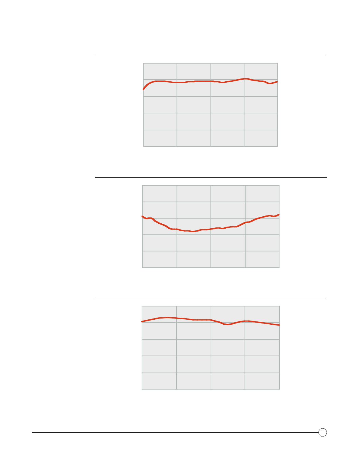
20- dBm Typical Output Power at 1
●
7.5-dB Typical Gain
●
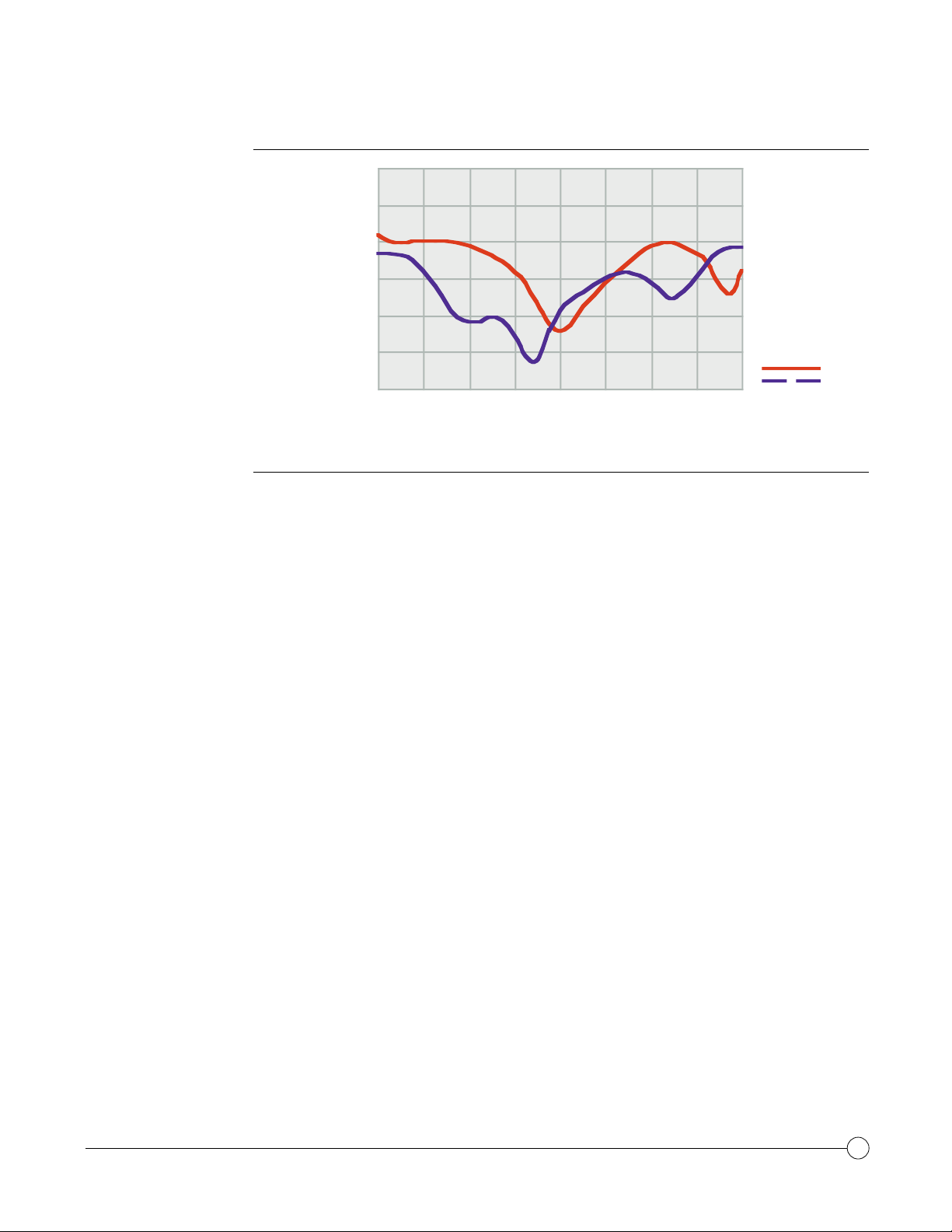
Input/Output SWR 1.5:1
●
On - Chip Blocking Capacitor Allows Easy Cascading
●
2,362 x 1,625 x 0,152 mm (0.093 x 0.064 x 0.006 in.)
●
-dB Gain Compression
DESCRIPTION
TriQuint Semiconductor, Inc. • Texas Facilities • (972) 995-8465
The TriQuint TGA8300 - SCC is a GaAs monolithic distributed amplifier designed for use as a
multioctave general - purpose gain block. Four 189 - µm gate width FETs provide 7.5 -dB nominal gain
and 5.5- dB noise figur e from 2 to 18- GHz. Typical power output is 20 - dBm at 1-dB gain compression.
Typical input and output SWRs are 1.5:1. Ground is provided to the circuitry through vias to the
backside metallization.
The TGA8300 - SCC is supplied in chip for m and is engineered for high -volume automated assembly .
All metal sur faces are gold plated to be compatible with ther mocompression and thermosonic
wire - bonding processes.
• www.triquint.com
Page 2
TGA8300-SCC
TYPICAL
SMALL-SIGNAL
POWER GAIN
TYPICAL
NOISE FIGURE
10
8
6
4
Gain (dB)
2
0
2 6 10 14 18
Frequency (GHz)
10
8
6
V+= 6 V
V+= 6 V
+
+
= 50% I
I
= 50% I
I
TA= 25°C
T A=25° C
V+= 6 V
V+= 6 V
+
+
= 50% I
I
= 50% I
I
T A=25° C
TA= 25°C
DSS
DSS
DSS
DSS
TYPICAL
OUTPUT POWER
P
1dB
4
Noise Figure (dB)
2
0
2 6 10 14 18
Frequency (GHz)
25
20
15
10
Output Power (dBm)
5
0
2 6 10 14 18
Frequency (GHz)
V+= 6 V
V+= 6 V
+
+
= 50% I
I
= 50% I
I
T A=25° C
TA= 25°C
DSS
DSS
TriQuint Semiconductor, Inc. • Texas Facilities • (972) 995-8465
• www.triquint.com
2
Page 3
TGA8300 -SCC
TYPICAL
RETURN LOSS
ABSOLUTE
MAXIMUM RATINGS
0
6
12
18
24
Return Loss (dB)
30
36
2 4 6 8 10 12 14 16 18
V+= 6 V
V += 6 V
+
+
= 50% I
I
= 50% I
I
T A=25° C
TA= 25°C
DSS
DSS
Input
Input
Output
Output
Frequency (GHz)
Positive supply voltage, V+ .................................................................................................................... 8 V
Negative supply voltage range, V–.............................................................................................. 0 V to -5 V
Power dissipation, PDat (or below) 25 C base-plate temperatur e* ...................................................... 1.8 W
Operating channel temperature, TCH** ......................................................... .....................................150 C
Mounting temperature (30 sec), TM .................................................................................................... 320 C
Storage temperature range, T
Ratings over operating channel temperature range, T
............................................................................................-65 to 150 C
STG
(unless otherwise noted)
CH
Stresses beyond those listed under “Absolute Maximum Ratings” may cause per manent damage to the device.
These are stress ratings only, and functional operation of the device at these or any oth er conditions beyond
those indicated under “RF Characteristics” is not implied. Exposure to absolute maximum rated conditions for
extended periods may affect device reliability.
* For operation above 25 C base-plate temperature, derate linearly at the rate of 3.8 mW/ C.
** Operating channel temperatur e directly affects the device MTTF . For maximum life, it is r ecommended that
channel temperature be maintained at the lowest possible level.
TriQuint Semiconductor, Inc. • Texas Facilities • (972) 995-8465
• www.triquint.com
3
Page 4

TGA8300-SCC
TYPICAL S-PARAMETERS
Frequency S
(GHz)
MAG ANG (° ) MAG ANG (°) MAG ANG (° ) MAG ANG (° ) (dB)
11
S
21
S
12
S
22
1.0 0.40 4 2.32 -146 0.017 -163 0.52 -110 7.3
1.5 0.40 -151 2.00 167 0.015 97 0.32 -172 6.0
2.0 0.28 180 2.20 155 0.017 91 0.20 109 6.8
2.5 0.26 167 2.34 137 0.022 75 0.20 56 7.4
3.0 0.25 158 2.41 121 0.027 59 0.20 27 7.6
3.5 0.25 151 2.45 105 0.031 40 0.18 10 7.8
4.0 0.25 143 2.46 89 0.033 25 0.15 -2 7.8
4.5 0.25 137 2.45 74 0.037 12 0.11 -10 7.8
5.0 0.25 132 2.44 60 0.040 -3 0.08 -13 7.7
5.5 0.24 127 2.42 46 0.043 -17 0.06 -11 7.7
6.0 0.23 122 2.42 32 0.045 -31 0.06 -9 7.7
6.5 0.21 116 2.41 19 0.048 -45 0.06 -10 7.6
7.0 0.19 112 2.43 5 0.051 -58 0.06 -16 7.7
7.5 0.17 106 2.45 -8 0.054 -72 0.06 -30 7.8
8.0 0.14 101 2.45 -22 0.058 -86 0.04 -44 7.8
8.5 0.11 97 2.45 -36 0.062
9.0
9.5
10.0
10.5
11.0
11.5
12.0
12.5
13.0
13.5
14.0
14.5
15.0
15.5
16.0
16.5
17.0
17.5
18.0
18.5
19.0
19.5
20.0
0.08
0.05
0.05
0.05
0.07
0.09
0.11
0.14
0.17
0.20
0.23
0.25
0.25
0.23
0.20
0.17
0.12
0.09
0.15
0.22
0.30
0.28
0.21
95
105
130
148
146
134
117
97
76
58
42
27
15
6
-1
-3
2
32
60
59
44
21
-8
2.46
2.47
2.46
2.45
2.44
2.42
2.43
2.46
2.49
2.51
2.54
2.54
2.51
2.47
2.46
2.44
2.39
2.40
2.44
2.53
2.64
2.62
2.44
-50
-64
-78
-92
-106
-120
-134
-148
-162
-177
-168
-152
-136
-121
-105
-90
-74
-58
-42
-24
4
-19
-42
0.066
0.070
0.075
0.079
0.082
0.086
0.091
0.095
0.100
0.104
0.109
0.113
0.114
0.115
0.115
0.116
0.116
0.119
0.125
0.136
0.150
0.155
0.151
-100
-113
-126
-139
-152
-165
-177
171
159
147
135
121
106
91
77
61
46
-3
15
-0
-16
-36
-59
-80
0.03
0.03
0.05
0.07
0.08
0.10
0.11
0.13
0.14
0.14
0.13
0.12
0.10
0.09
0.10
0.13
0.17
0.21
0.23
0.23
0.19
0.12
0.11
0.19
-81
-143
174
148
126
105
82
60
38
17
-4
-32
-66
-110
-158
165
134
116
98
80
66
65
100
107
GAIN
7.8
7.8
7.8
7.8
7.8
7.7
7.7
7.7
7.8
7.9
8.0
8.1
8.1
8.0
7.9
7.8
7.7
7.6
7.6
7.7
8.1
8.4
8.4
7.7
V+= 6 V, I+= 50% I
Reference planes for S - parameter data include bond wires as specified in the “Recommended Assembly
Diagram.”
TriQuint Semiconductor, Inc. • Texas Facilities • (972) 995-8465
, TA= 25°C
DSS
• www.triquint.com
4
Page 5

TGA8300-SCC
RF CHARACTERISTICS
DC CHARACTERISTICS
THERMAL INFORMATION
PARAMETER TEST CONDITIONS TY P UNIT
G
P
Small–signal power gain f = 2 to 18 GHz 7.5 dB
SWR(in) Input standing wave ratio f = 2 to 18 GHz 1.5:1 SWR(out) Output standing wave ratio f t = 2 o 18 GHz 1.4:1 P
1dB
Output power at 1–dB gain compression f = 2 to 18 G Hz 20 dBm
NF Noise figure f = 2 to 18 GHz 5.5 dB
f = 8 GHz 32
IP
3
Output third–order intercept point f = 12 GH z 28 dB m
f = 18 G Hz 27
V+= 6 V, I+= 50% I
PARAMETER TEST CONDITIONS MIN MAX UNIT
I
Total zero–gate–voltage drain current V DS = 0.5 V to 3.5 V, V GS = 0 130 300 mA
DSS
, TA= 25°C
DSS
at saturation
TA= 25°C
VDSfor I
is the drain voltage between 0.5 V and 3.5 V at which drain current is highest at DC autoprobe.
DSS
PARAMETER TEST CONDITIONS NO M UNIT
R
Thermal resistance, channel–to–backside V + = 6 V, I+ = 50% I
JC
DSS
45 °C/W
EQUIVALENT
SCHEMATIC
RECOMMENDED TEST
CONFIGURATION
Input
+
V
FET 2 FET 1
189 m
RF
189 m
DC Block
FET 3
189 m
FET 4
189 m
DUTRF Input RF Output
RF
Output
-
V
TriQuint Semiconductor, Inc. • Texas Facilities • (972) 995-8465
• www.triquint.com
5
Page 6

TGA8300-SCC
TYPICAL BIAS NETWORK
RECOMMENDED
ASSEMBLY DIAGRAM
V+= 6 V
R
d-Q
C
Bypass
2
4
0.01 F
3
C
Bypass
RF OutputRF Input
-
V
= -1 V
1
TGA8300
C
Block
+
V
25
RF Input
RF connections: Bond using three 1- mil diameter, 20 to 30-mil-length gold bond wires at RF input and two 1 - mil
diameter, 20 to 30 - mil- length gold bond wires at RF output for optimum RF per formance.
Close placement of external components is essential to stability .
TriQuint Semiconductor, Inc. • Texas Facilities • (972) 995-8465
0.01 F
• www.triquint.com
RF Output
-
V
6
Page 7

TGA8300-SCC
MECHANICAL DRAWING
1,6256
(0.0640)
1,4199
(0.0559)
0,1803
(0.0071)
2,2047
(0.0868)
2,2073
(0.0869)
3
4
2,3622
(0.0930)
1,1227
(0.0442)
0,3073
(0.0121)
0,1702
(0.0067)
2
1
0
0,1524
0
(0.0060)
Units: millimeters (inches)
Thickness: 0,1524 (0.0060) (reference only)
Chip edge to bond pad dimensions are shown to center of bond pad.
Chip size tolerance: ± 0,0508 (0.0020)
Bond pad #1 (RF Input): 0,1270 x 0,1016 (0.0050 x 0.0040)
Bond pad #2 (V
Bond pad #3 (RF Output): 0,1321 x 0,1016 (0.0052 x 0.0040)
Bond pad #4 (V
+
): 0,1575 x 0,1245 (0.0062 x 0.0049)
–
): 0,0635 (0.0025) (radius)
TriQuint Semiconductor, Inc. • Texas Facilities • (972) 995-8465
• www.triquint.com
7
 Loading...