

Page 1
Product Data Sheet
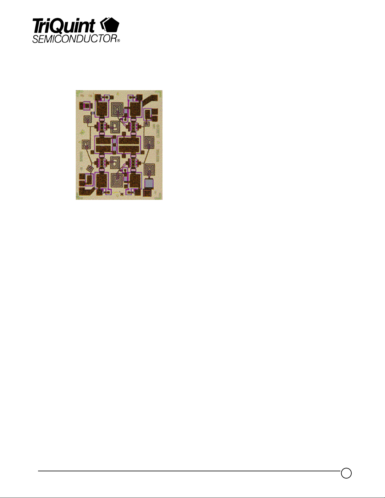
2 - 6 GHz Gain Block Amplifier TGA8226-SCC
Key Features and Performance
• 2 to 6 GHz Frequency Range
• 13.5 dB Gain
• 17 dBm Output Power at 1 dB Gain
Compression
• 5.5 dB Noise Figure
• Operates from Single 15V Supply
• 1.47 x 1.85 x 0.15 mm (0.058 x 0.073 x
0.006 in.)
Description
The TriQuint TGA8226-SCC is a self biased distributed amplifier and operates from
a single 15 V supply. Four 457 um FETs produce a typical gain greater than 13.5
dB, with input and output SWRs less than 2:1. Direct cascading without additional
components is possible by using the on-chip blocking capacitors. Ground is
provided to the circuitry through vias to the backside metallization.
Bond pad and backside metallization is gold plated for compatibility with eutectic
alloy attachment methods as well as thermocompression and thermosonic wirebonding processes. The TGA8226-SCC is available in chip form and is readily
assembled using automated equipment.
TriQuint Semiconductor Texas Phone: (972)994 8465 Fax: (972)994 8504 Web: www.triquint.com
1
Page 2
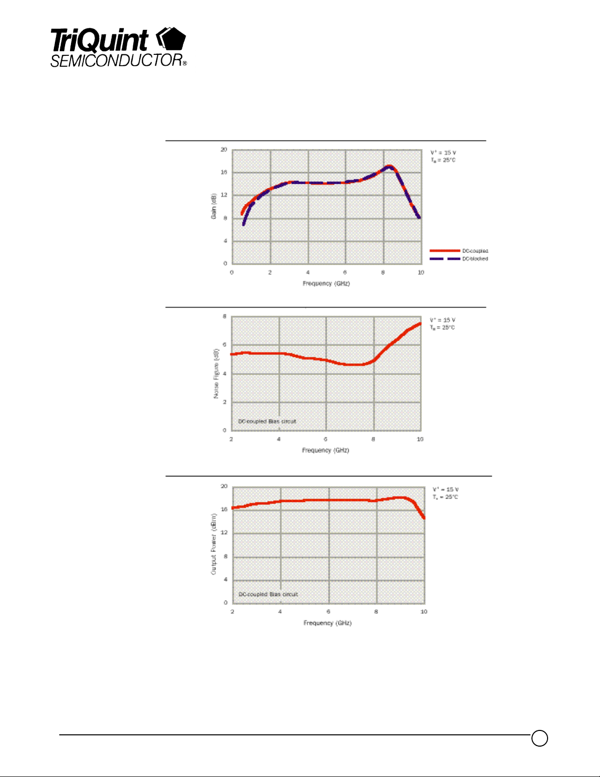
TYPICAL
SMALL-SIGNAL
POWER GAIN
Product Data Sheet
TGA8226-SCC
TYPICAL
NOISE FIGURE
TYPICAL
OUTPUT POWER
P
1dB
TriQuint Semiconductor Texas Phone: (972)994 8465 Fax: (972)994 8504 Web: www.triquint.com
2
Page 3
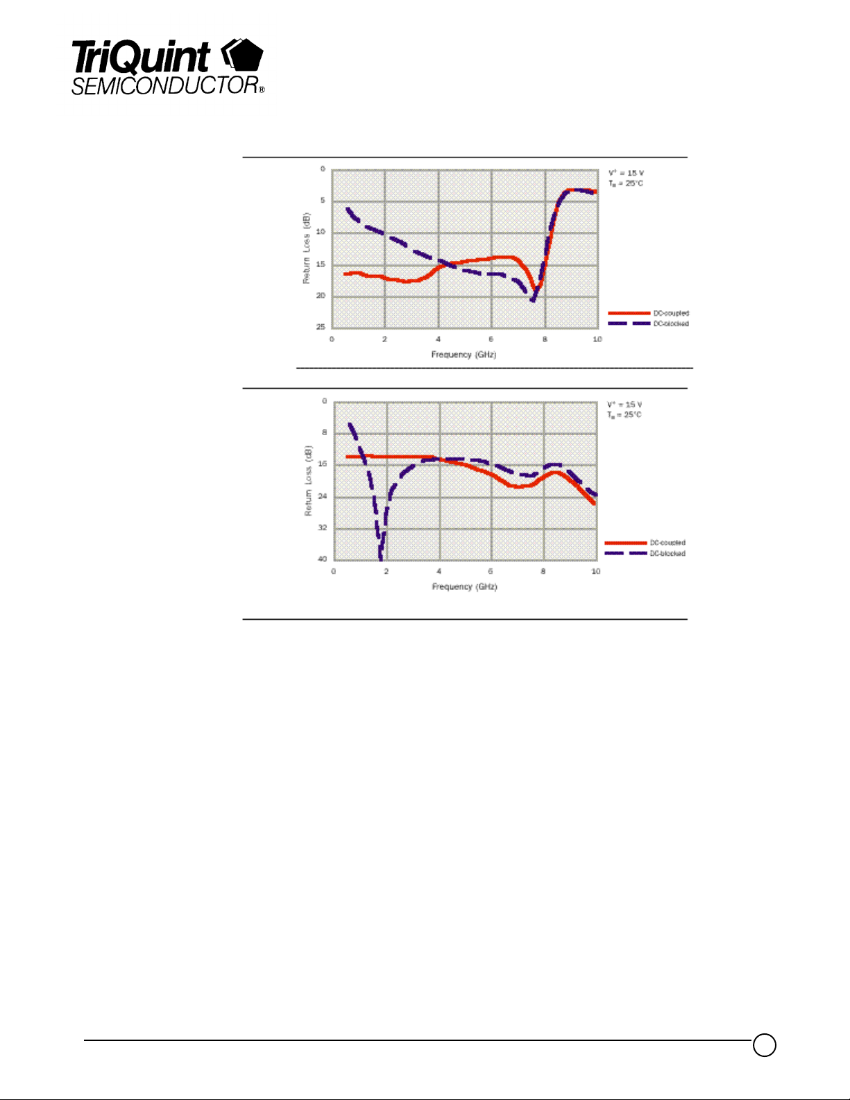
TYPICAL
…
/
INPUT RETURN LOSS
TYPICAL
OUTPUT RETURN LOSS
Product Data Sheet
TGA8226-SCC
ABSOLUTE
MAXIMUM
RATINGS
TriQuint Semiconductor Texas Phone: (972)994 8465 Fax: (972)994 8504 Web: www.triquint.com
Positive supply voltage, V+…………………………………………………………………………… 18 V
Pow er dissipation, P
Input continuous-w ave pow er, P
Operating Channel temperature, T
Mounting temperature (30 sec.), T
Storage temperature range, T
Ratings over operating channel temperature range, T
at (or below) 25oC base-plate temperature *………………………………
D
…………………………………………………………………
IN
**…………………………………………………………………150oC
CH
……………………………………………………………………320oC
M
………………………………………………………………………-65 to 150oC
STG
(unless otherwise note d).
CH
4.4 W
23 dB
Stresses beyond those listed under "A bsolute Maximum Ratings" may cause per manent damage to the device.
These are stress ratings only and f unctional operation of the device at these or any other conditions beyond
those indicated under "RF Charac teristics" is not implied. Exposure to abs olute maximum rated conditions
for extended periods may af f ect device reliability.
o
* For operation abov e 25
C base-plate temperature, derate linearly at the rate of 9.2 mW
** Operating channel temperature ( T
) directly affects the device MTTF. For maximum life, it is recommended
CH
o
C.
that channel temperature be maintained at the low est possible level.
3
Page 4

Product Data Sheet
TGA8226-SCC
TYPICAL S-PARAMETERS
Freque ncy
(GHz) MAG ANG(°) MAG ANG(°) MAG ANG(°) MAG ANG(°) (dB)
S
11
S
21
S
12
S
22
0.5 0.15 7 2.70 21 0.000 30 0.21 153 8.6
1.0 0.15 -20 3.47 -6 0.001 104 0.20 125 10.8
1.5 0.14 -44 4.01 -27 0.001 124 0.21 100 12.1
2.0 0.14 -73 4.49 -49 0.002 124 0.20 80 13.1
2.5 0.13 -104 4.89 -72 0.004 119 0.20 62 13.8
3.0 0.13 -133 5.14 -95 0.006 110 0.20 48 14.2
3.5 0.14 -155 5.15 -118 0.009 88 0.20 34 14.2
4.0 0.16 -174 5.10 -139 0.008 64 0.19 22 14.2
4.5 0.18 169 5.07 -160 0.007 57 0.17 12 14.1
5.0 0.19 157 5.06 180 0.008 50 0.16 0 14.1
5.5 0.19 148 5.08 160 0.008 37 0.14 -12 14.1
6.0 0.20 140 5.13 140 0.008 21 0.12 -21 14.2
6.5 0.20 130 5.27 119 0.008 -5 0.10 -24 14.4
7.0 0.19 111 5.49 98 0.008 -33 0.08 -14 14.8
7.5 0.13 73 5.97 75 0.011 -68 0.09 -10 15.5
8.0 0.16 -38 6.73 46 0.017 -106 0.11 -24 16.6
8.5 0.50 -117 7.01 3 0.023 -154 0.13 -73 16.9
9.0 0.69 -168 5.07 -38 0.022 165 0.10 -128 14.1
9.5 0.69 162 3.37 -65 0.018 141 0.07 -160 10.6
10.0 0.65 144 2.38 -86 0.015 128 0.05 176 7.5
V+ = 15 V, TA = 25oC, DC-coupled bias and external DC blocks
GAIN
RF CHARACTERISTICS
DC CHARACTERISTICS
Reference planes for S-parameter data include bond wires as specified in the “Recommended
Assembly Diagram”. The S-parameters are also available on floppy disk and the world wide web.
P ARAMETER TEST CONDITIONS TYP UNIT
G
p
Small–s ignal pow er gain f = 2 to 6 GHz 13.5 dB
SWR(in) Input s tanding w ave ratio f = 2 to 6 GHz 1.4:1 -
SWR(out) Output standing w a ve ra tio f = 2 to 6 GHz 1.4:1 P
1dB
Output pow e r a t 1–dB gain c ompres s ion f = 2 to 6 GHz 17 dBm
NF Nois e figure f = 2 to 6 GHz 5.5 dB
f = 2 GHz 26
IP
3
Output third–orde r interc e pt point f = 4 GHz 28 dBm
f = 6 GHz 27
V+ = 15 V, TA = 25oC, DC-coupled bias and external DC blocks
+
I
P ARAMETER TEST CONDITIONS TYP UNIT
Positive s upply current
= 25oC
T
A
+
V
= 15 V T
= 25°C
A
68 mA
TriQuint Semiconductor Texas Phone: (972)994 8465 Fax: (972)994 8504 Web: www.triquint.com
4
Page 5

EQUIVALENT
SCHEMATIC
Product Data Sheet
TGA8226-SCC
TYPICAL BIAS
NETWORK
(DC-Blocked Bias Circuit) (DC-Coupled Bias Circuit)
TriQuint Semiconductor Texas Phone: (972)994 8465 Fax: (972)994 8504 Web: www.triquint.com
5
Page 6

RECOMMENDED
ASSEMBLY DIAGRAM
DC-Blocked Bias Circuit
Product Data Sheet
TGA8226-SCC
RF connections: Bond using 1-mil diameter, 15-mil-length gold bond wires at both RF Input and RF Output
for optimum RF performance.
Close placement of external components is essential to stability.
Refer to TriQuint’s Recommended Assembly Instructions for GaAs Products.
TriQuint Semiconductor Texas Phone: (972)994 8465 Fax: (972)994 8504 Web: www.triquint.com
6
Page 7

RECOMMENDED
ASSEMBLY DIAGRAM
DC-Coupled Circuit
Product Data Sheet
TGA8226-SCC
RF connections: Bond using 1-mil diameter, 15-mil-length gold bond wires at both RF Input and RF Output
for optimum RF performance.
Close placement of external components is essential to stability.
Refer to TriQuint’s Recommended Assembly Instructions for GaAs Products.
GaAs MMIC devices are susceptible to damage from Electrostatic Discharge. Proper precautions should be observed
during handling, assembly and test.
TriQuint Semiconductor Texas Phone: (972)994 8465 Fax: (972)994 8504 Web: www.triquint.com
7
Page 8

Product Data Sheet
TGA8226-SCC
GaAs MMIC devices are susceptible to damage from Electrostatic Discharge. Proper precautions should be observed
during handling, assembly and test.
TriQuint Semiconductor Texas Phone: (972)994 8465 Fax: (972)994 8504 Web: www.triquint.com
8
 Loading...