

Page 1

Product Data Sheet
Gain Block Amplifier TGA8161-SCC
Key Features and Performance
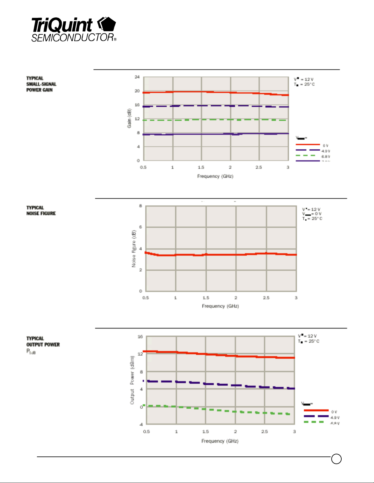
• 500 MHz to 3 GHz Frequency Range
• 19 dB Gain with 3.5 dB Noise Figure
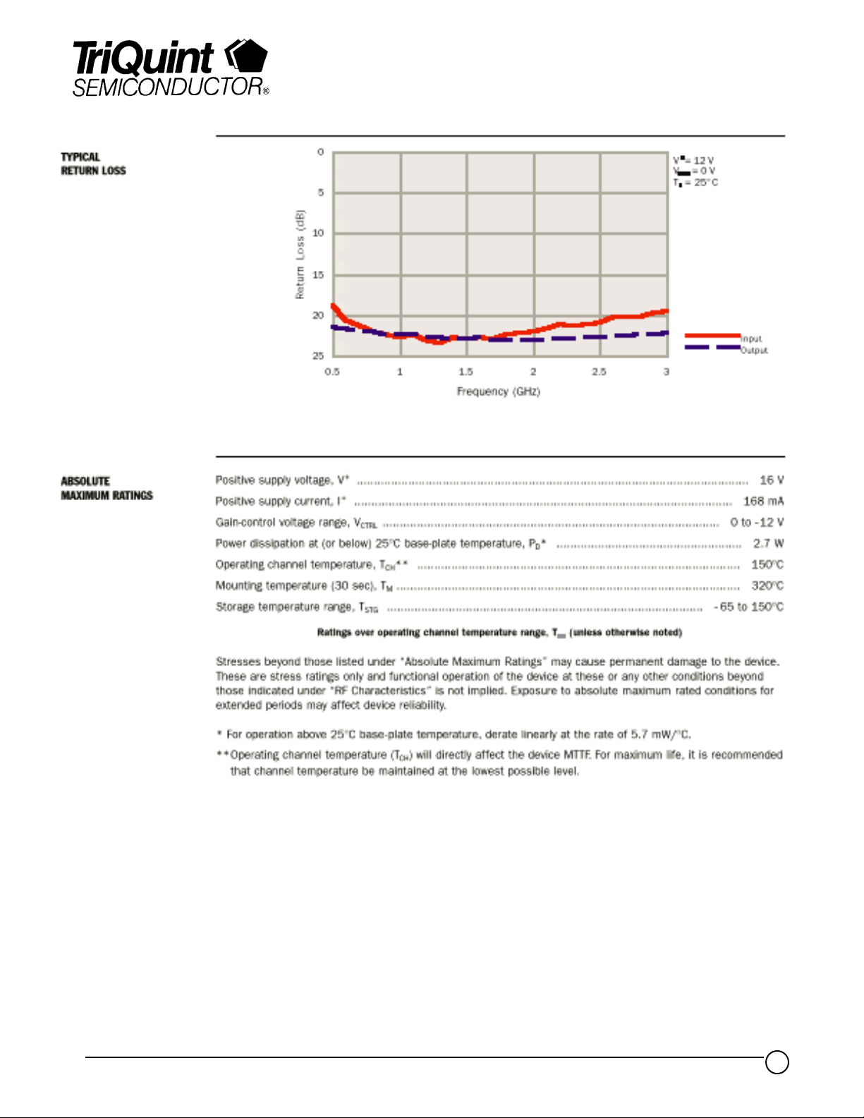
• 1.5:1 input/Output SWR
• Operates from Single 12 V Supply
• Greater than 10 dB Flat Gain Control
Range
• Unconditionally Stable
• 1.060 x 0.9398 x 0.1524 mm (0.040 x
0.037 x 0.006 in.)
Description
The TriQuint TGA8161-SCC is a monolithic 3-stage general purpose 500 MHz to 3
GHz amplifier designed as a complementary product to the TGA8061-SCC, 0.1 to 3.5
GHz amplifier.
The TGA8161-SCC is a self-biased amplifier with gain control capability, reduced
power consumption, and 3 dB bandwidth performance over the 100 MHz to 4 GHz
band. Typical output power at 1 dB gain compression is 12 dBm. The TGA8161-SCC
is ideal for receiver applications and may be used in gain control or switching
applications.
The TGA8161-SCC is supplied in chip form, with backside metallization, for ease of
assembly.
TriQuint Semiconductor Texas : (972)994 8465 Fax: (972)994 8504 Web: www.triquint.com
1
Page 2
Product Data Sheet
TGA8161-SCC
TriQuint Semiconductor Texas : (972)994 8465 Fax: (972)994 8504 Web: www.triquint.com
2
Page 3
Product Data Sheet
TGA8161-SCC
TriQuint Semiconductor Texas : (972)994 8465 Fax: (972)994 8504 Web: www.triquint.com
3
Page 4

Product Data Sheet
TGA8161-SCC
TYPICAL S-PARAMETERS
Frequency
(G Hz ) MAG ANG ( °) MAG ANG (°) MAG ANG ( °) MAG ANG (°) (d B)
S
11
S
21
S
12
S
22
0.1 0.48 - 92 5.50 44 0.0120 - 75 0.14 - 6 14.8
0.2 0.19 - 97 7.68 24 0.0044 - 90 0.12 - 29 17.7
0.3 0.17 - 116 8.56 12 0.0024 - 93 0.10 - 34 18.6
0.4 0.13 - 126 8.96 3 0.0014 - 87 0.09 - 35 19.0
0.5 0.11 - 142 9.18 - 4 0.0007 - 94 0.09 - 33 19.3
0.6 0.09 - 152 9.32 - 10 0.0002 - 58 0.08 - 35 19.4
0.7 0.09 - 158 9.40 - 15 0.0002 89 0.08 - 37 19.5
0.8 0.08 - 173 9.46 - 21 0.0007 84 0.08 - 40 19.5
0.9 0.08 - 178 9.50 - 26 0.0010 75 0.08 - 43 19.6
1.0 0.07 170 9.53 - 30 0.0012 84 0.08 - 46 19.6
1.1 0.08 160 9.54 - 35 0.0016 81 0.08 - 50 19.6
1.2 0.07 151 9.55 - 39 0.0018 81 0.07 - 53 19.6
1.3 0.07 146 9.56 - 44 0.0022 82 0.07 - 55 19.6
1.4 0.07 135 9.54 - 48 0.0024 85 0.07 - 60 19.6
1.5 0.07 128 9.53 - 53 0.0027 83 0.07 - 63 19.6
1.6 0.07 121 9.51 - 57 0.0028 82 0.07 - 67 19.6
1.7 0.07 111 9.50 - 61 0.0031 83 0.07 - 71 19.6
1.8 0.08 105 9.47 - 66 0.0033 81 0.07 - 76 19.5
1.9 0.08 99 9.43 - 70 0.0036 81 0.07 - 80 19.5
2.0 0.08 90 9.40 - 74 0.0037 80 0.07 - 85 19.5
2.1 0.08 84 9.31 - 79 0.0040 79 0.07 - 89 19.4
2.2 0.09 78 9.28 - 83 0.0042 78 0.07 - 94 19.4
2.3 0.09 71 9.22 - 87 0.0045 78 0.07 - 98 19.3
2.4 0.09 65 9.15 - 92 0.0047 78 0.07 - 104 19.2
2.5 0.09 60 9.07 - 96 0.0048 78 0.07 - 109 19.1
2.6 0.10 53 8.97 - 100 0.0050 77 0.08 - 114 19.1
2.7 0.10 47 8.86 - 105 0.0052 76 0.08 - 118 18.9
2.8 0.10 43 8.77 - 109 0.0055 76 0.08 - 123 18.9
2.9 0.10 35 8.64 - 113 0.0057 74 0.08 - 127 18.7
3.0 0.11 29 8.52 - 117 0.0058 73 0.08 - 131 18.6
3.1 0.11 23 8.41 - 122 0.0059 74 0.08 - 135 18.5
3.2 0.11 17 8.27 - 126 0.0061 74 0.08 - 139 18.3
3.3 0.11 11 8.14 - 130 0.0062 72 0.08 - 143 18.2
3.4 0.12 6 7.99 - 135 0.0063 73 0.09 - 148 18.1
3.5 0.12 0 7.82 - 139 0.0064 72 0.09 - 152 17.9
3.6 0.12 - 6 7.66 - 143 0.0065 72 0.09 - 155 17.7
3.7 0.12 - 12 7.51 - 147 0.0066 69 0.09 - 158 17.5
3.8 0.13 - 18 7.35 - 151 0.0066 72 0.09 - 162 17.3
3.9 0.13 - 23 7.18 - 155 0.0069 70 0.09 - 165 17.1
4.0 0.13 - 28 7.02 - 159 0.0070 72 0.10 - 169 16.9
GAIN
+
= 12 V, V
V
= 0 V, TA = 25O C
CTRL
Reference planes for S-parameter data include bond wires as specified in the “Recommended
Assembly Diagram”. The S-parameters are also available on floppy disk and the world wide web.
TriQuint Semiconductor Texas : (972)994 8465 Fax: (972)994 8504 Web: www.triquint.com
4
Page 5

Product Data Sheet
n
TGA8161-SCC
RF CHARACTERISTICS
DC CHARACTERISTICS
PARAMETER TEST CONDITIONS TYP UNIT
G
p
Small–signal power gain f = 0.5 to 3 GHz 19 dB
G
p
∆
P
Gain flatness f = 0.5 to 3 GHz ± 0.5 dB
= - 55°C to 90°C
T
BP
Gain temperature coefficient
1dB
Output power at 1–dB gain compressio
f = 0.5 to 3 GHz 12 dBm
-0.01 dB/°C
NF Noise figure f = 0.5 to 3 GHz 3.5 dB
0.5 GHz 21
IP
3
Output third–order intercept point 1.5 GHz 21 dBm
3 GHz 20.5
+
= 12 V, V
V
= 0 V, TA = 25o C
CTRL
PARAMETER TEST CONDITIONS TYP UNIT
+
I
for I
V
ds
highest.
I
DSS
+
V
= 12 V, V
is the drain voltage between .5V and 3.5 V at which drain current is
dss
= 0 V, TA = 25oC
CTRL
V
= .5 V to 3.5 V, V
DS
= 0 V 81.2 mA
GS
TriQuint Semiconductor Texas : (972)994 8465 Fax: (972)994 8504 Web: www.triquint.com
5
Page 6

Product Data Sheet
TGA8161-SCC
TriQuint Semiconductor Texas : (972)994 8465 Fax: (972)994 8504 Web: www.triquint.com
6
Page 7

Product Data Sheet
TGA8161-SCC
GaAs MMIC devices are susceptible to damage from Electrostatic Discharge. Proper precautions should be observed during
handling, assembly and test.
TriQuint Semiconductor Texas : (972)994 8465 Fax: (972)994 8504 Web: www.triquint.com
7
 Loading...