

Page 1
Advance Product Information
Feb 4, 2000
18-27.5 GHz 1W Power Amplifier TGA1135B
Key Features
• 0.25 um pHEMT Technology
• 14 dB Nominal Gain at 23GHz
• 30 dBm Nominal P1dB
• 38dBm OTOI typical
• Typical 15dB Input/Output RL
• Bias 6 - 7V @ 540 mA
• On-chip power detector diode
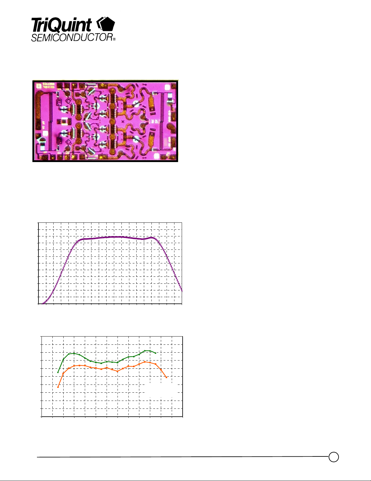
Chip Dimensions 2.641 mm x 1.480 mm
TGA1135B Fixtured Amplifier Typical Small Signal Data
18
16
14
12
10
8
6
S21 (dB)
4
2
0
-2
-4
-6
13 14 15 16 17 18 19 20 21 22 23 24 25 26 27 28 29 30 31 32
32
31.5
31
30.5
30
29.5
P1dB (dBm)
29
28.5
28
27.5
27
16 17 18 19 20 21 22 23 24 25 26 27 28 29
Wafer 993150303, 6V/540mA
Frequency (GHz)
TGA1135B Nominal Ou tput Power
Wafer 993150303, Idq=540mA
Frequency (GHz)
VD = 7V
Note: 1 dB of
compress ion not
reached on some parts
at 27, 27.5 GHz
Primary Applications
• Point-to-Point Radio
• Point-to-Multipoint Communications
• Ka Band Sat-Com
VD = 6V
Note: Devices designated as EPU are typically early in their characterization process prior to finalizing all electrical and process
specifications. Specifications are subject to change without notice
TriQuint Semiconductor Texas : Phone (972)994-8465 Fax (972)994 8504 Web: www.triquint.com
1
Page 2
Advance Product Information
,
Feb 4, 2000
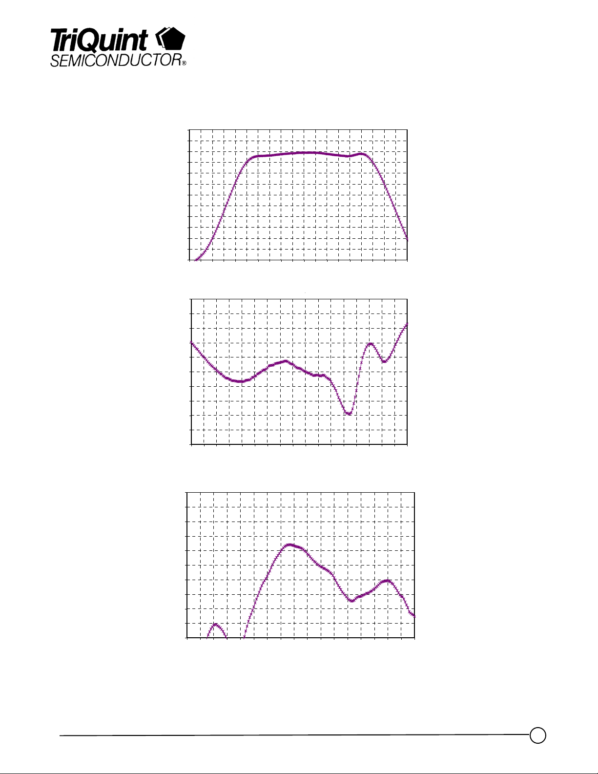
S21
S11
Measured small signal data
6V, 540mA
18
16
14
12
10
8
6
S21 (dB)
4
2
0
-2
-4
-6
13 14 15 16 17 18 19 20 21 22 23 24 25 26 27 28 29 30 31 32
-5
-7
-9
-11
-13
-15
S11 (dB)
-17
-19
-21
-23
-25
15 16 17 18 19 20 21 22 23 24 25 26 27 28 29 30 31 32
Frequency (GH z)
Frequency (GHz)
TGA1135B
-5
-7
-9
-11
-13
S22
-15
S22 (dB)
-17
-19
-21
-23
-25
15 16 17 18 19 20 21 22 23 24 25 26 27 28 29 30 31 32
Frequency (GHz)
Note: Devices designated as EPU are typically early in their characterization process prior to finalizing all electrical and process
specifications. Specifications are subject to change without notice.
TriQuint Semiconductor Texas : Phone (972)994-8465 Fax (972)994 8504 Web: www.triquint.com
2
Page 3
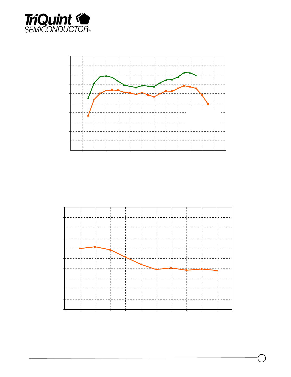
32
31.5
31
30.5
Advance Product Information
Feb 4, 2000
TGA1135B
TGA1135B Nominal Output Power
Wafer 993150303, Idq=540mA
VD = 7V
30
29.5
P1dB (dBm)
29
28.5
28
27.5
27
16 17 18 19 20 21 22 23 24 25 26 27 28 29
Frequency (GHz)
Note: 1 dB of
compression not
reached on some parts
at 27, 27.5 GHz
P1dB Measured Data
TOI performance @ Pin SCL=7dBm: Vd=6V, Id=540mA, separation = 10MHz
43
42
41
TGA1135B wafer 993150303 nominal performance
VD = 6V
40
39
38
TOI (dBm)
37
36
35
34
33
17 18 19 20 21 22 23 24 25 26 27 28
Frequency (GHz)
Output TOI Measured Data
Note: Devices designated as EPU are typically early in their characterization process prior to finalizing all electrical and process
specifications. Specifications are subject to change without notice.
TriQuint Semiconductor Texas : Phone (972)994-8465 Fax (972)994 8504 Web: www.triquint.com
3
Page 4

Advance Product Information
VG1 VG2 GND DQ VD
Q1a Q2a
Feb 4, 2000
TGA1135B
DET
OUT
600µµµµm
RF IN
Q1b
600µµµµm
Reference
diode 2
REF3 GND VG1 VG2 GND DQ
Note: no DC current
allowed into the “DQ” pad
Q2b
1200µµµµm
1200µµµµm
Note:
drains not
connected
on lot
9931503
VD
Note: If drain bias is from one side
only, maximum Id is 440mA
PWR
DET
RF OUT
Reference
diode 1
REF2REF1
DC Schematic
Note: Devices designated as EPU are typically early in their characterization process prior to finalizing all electrical and process
specifications. Specifications are subject to change without notice.
TriQuint Semiconductor Texas : Phone (972)994-8465 Fax (972)994 8504 Web: www.triquint.com
4
Page 5

0.686
RF IN
Advance Product Information
Feb 4, 2000
TGA1135B
m)
µ
µ
µ
µ
DET
OUT
0.095
0.612: VG2
0.875: DQ
1.253: VD
(180x100
2.543
2.641
1.480
0.833
PWR DET
(175x100
µµµµ
m)
0.000
0.000
REF 1: 0.220
Dimensions in mm
RF I/O Pad: 200x100 mm
DC Pads: 105x105 mm
Die Area: 3.909 mm
2
VG2: 0.612
DQ: 0.875
0.373
RF OUT
0.098
m)
µ
µ
µ
µ
VD: 1.253
(180x100
REF 2: 2.543
REF 3: 2.360
Note: Devices designated as EPU are typically early in their characterization process prior to finalizing all electrical and process
specifications. Specifications are subject to change without notice.
TriQuint Semiconductor Texas : Phone (972)994-8465 Fax (972)994 8504 Web: www.triquint.com
5
Page 6

Advance Product Information
TGA1135B built-in power detector
Feb 4, 2000
TGA1135B
V
det
100pF
RF
IN
TGA1135B with external test coupler
(amplifier bias connections not shown)
On-chip diode functions as envelope detector
External coupler and DC bias required
100pF
V
bias
RF
OUT
ΩΩΩΩ
EG1135B measured detector voltage offset vs output power with
20dB coupler: Vb=0.8V, f = 20GHz, Coupler loss is uncalibrated,
10
1
0.1
Detector voltage (V)
0.01
8 101214161820222426283032
Note: Devices designated as EPU are typically early in their characterization process prior to finalizing all electrical and process
specifications. Specifications are subject to change without notice.
ΩΩΩΩ
10K
Pout (dBm)
load
10K
Video out
(V
)
det
EG1135B
C=2pF
RF
OUT
External
DC bias
External coupler
TriQuint Semiconductor Texas : Phone (972)994-8465 Fax (972)994 8504 Web: www.triquint.com
(-20dB)
50
ΩΩΩΩ
RF
OUT
6
Page 7

Vg (optional)
0.01µµµµF
0.01µµµµF
DQ
Advance Product Information
Feb 4, 2000
TGA1135B
Vd
Input TFN
Vg
100pF
100pF
0.01µµµµF
DQ
0.01µµµµF
100pF
100pF
Vd
Output TFN
Notes:
1. 1µµµµF capacitor on gate, drain lines not
shown but required
2. 0.01µµµµF capacitor may be connected to
“DQ” port as shown, or may be included
on drain line
3. Vg connection is recommended on
both sides for devices operating at or
above P1dB
Chip Assembly and Bonding Diagram
GaAs MMIC devices are susceptible to damage from Electrostatic Discharge. Proper precautions should
be observed during handling, assembly and test.
Note: Devices designated as EPU are typically early in their characterization process prior to finalizing all electrical and process
specifications. Specifications are subject to change without notice.
TriQuint Semiconductor Texas : Phone (972)994-8465 Fax (972)994 8504 Web: www.triquint.com
7
Page 8

Advance Product Information
Assembly Process Notes
Reflow process assembly notes:
•=
AuSn (80/20) solder with limited exposure to temperatures at or above 300ΓC
•=
alloy station or conveyor furnace with reducing atmosphere
•=
no fluxes should be utilized
•=
coefficient of thermal expansion matching is critical for long-term reliability
•=
storage in dry nitrogen atmosphere
Component placement and adhesive attachment assembly notes:
•=
vacuum pencils and/or vacuum collets preferred method of pick up
•=
avoidance of air bridges during placement
•=
force impact critical during auto placement
•=
organic attachment can be used in low-power applications
•=
curing should be done in a convection oven; proper exhaust is a safety concern
•=
microwave or radiant curing should not be used because of differential heating
•=
coefficient of thermal expansion matching is critical
Feb 4, 2000
Interconnect process assembly notes:
•=
thermosonic ball bonding is the preferred interconnect technique
•=
force, time, and ultrasonics are critical parameters
•=
aluminum wire should not be used
•=
discrete FET devices with small pad sizes should be bonded with 0.0007-inch wire
•=
maximum stage temperature: 200ΓC
GaAs MMIC devices are susceptible to damage from Electrostatic Discharge. Proper precautions should
be observed during handling, assembly and test.
Note: Devices designated as EPU are typically early in their characterization process prior to finalizing all electrical and process
specifications. Specifications are subject to change without notice.
TriQuint Semiconductor Texas : Phone (972)994-8465 Fax (972)994 8504 Web: www.triquint.com
8
 Loading...