

Page 1
36 - 40 GHz Power Amplifier TGA1071-EPU
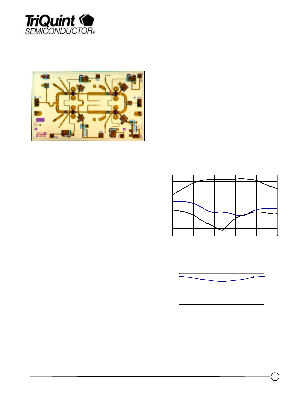
The TriQuint TGA1071-EPU is a two stage
PA MMIC design using TriQuint’s proven
0.25 um Power pHEMT process to support a variety
of millimeter wave applications including
point-to-point digital radio and point-to-multipoint
systems.
The two-stage design consists of two 300 um input
devices driving a pair of 400 um output devices.
The TGA1071 provides 22dBm of output power
across 36-40 GHz with a typical small signal gain
of 15dB.
The TGA1071 requires minimum off-chip
components. Each device is 100% DC and RF
tested on-wafer to ensure performance compliance.
The device is available in chip form.
Advance Product Information
Key Features and Performance
• 0.25um pHEMT Technology
• 36-40 GHz Frequency Range
• 22 dBm Nominal Pout @ P1dB
• 15 dB Nominal Gain
• 5V, 120 mA Bias
• Chip Dimensions 3.4mm x 2.1mm
Primary Applications
• Point-to-Point Radio
• Point-Multipoint Radio
TGA1071 Typical RF Performance (Fixtured)
20
15
10
5
0
-5
-10
Gain and Return Loss (dB)
-15
-20
-25
32.0 33.0 34.0 35.0 36.0 37.0 38.0 39.0 40.0 41.0 42.0
25.00
s11
s22
Frequency (GHz)
Small Signal Gain
TGA1071 RF Probe Summary Data
20.00
15.00
10.00
Pout (dBm)
5.00
0.00
36 37 38 39 40
Frequency (GHz)
Pout at 1dB Gain Compression
Note: Devices designated as EPU are typically early in their characterization process prior to finalizing all electrical and process
specifications. Specifications subject to change without notice
TriQuint Semiconductor Texas : Phone (972)994 8465 Fax (972)994 8504 Web: www.triquint.com
1
1
Page 2
Advance Product Information
+
D
IN
CH
M
STG
P1-5
GS1
GD1-5
p
Note: RF probe data is taken at 0.4 GHz steps
Electrical Characteristics
RECOMMENDED MAXIMUM RATINGS
Symbol Parameter Value Notes
+
V
I
P
P
T
T
T
1/ These ratings apply to each individual FET
2/ Junction operating temperature will directly affect the device mean time to failure
(MTTF). For maximum life it is recommended that junction temperatures be
maintained at the lowest possible levels.
3/ Total current for both stages
Positive Supply Voltage 7 V
Positive Supply Current .4 A 3/
Power Dissipation 2.8 W
Input Continuous Wave Power 20 dBm
Operating Channel Temperature
Mounting Temperature (30 seconds)
Storage Temperature
150 °C
320 °C
-65 °C to 150 °C
1/, 2/
DC PROBE TESTS
(TA = 25 °C ± 5°C)
Symbol Parameter Minimum Maximum Value
Idss Saturated Drain Current (info
140 658 mA
only)
V
BV
BV
Pinch-off Voltage -1.5 -0.5 V
Breakdown Voltage gate-source -30 -8 V
Breakdown Voltage gate-drain -30 -8 V
ON-WAFER RF PROBE CHARACTERISTICS
(TA = 25 °C ± 5°C)
Symbol Parameter Test Condition
Limit
Units
Vd=5V, Id=120mA
Min Nom Max
G
Small-signal
Power Gain
F = 36 to 40 GHz
F = 38 GHz 13
15 dB
dB
dB
IRL Input Return
F = 36 to 40 GHz - -10 - dB
Loss
ORL Output Return
F = 36 to 40 GHz - -10 - dB
Loss
PWR Output Power F = 36 to 40 GHz 22 - dBm
Note: Devices designated as EPU are typically early in their characterization process prior to finalizing all electrical and process
specifications. Specifications are subject to change without notice.
TriQuint Semiconductor Texas : Phone (972)994 8465 Fax (972)994 8504 Web: www.triquint.com
2
Page 3

Advance Product Information
Statistical Performance Summary
TGA1071 RF Probe Summary Data
14
12
10
8
6
Gain (dB)
4
2
0
36.0 36.4 36.8 37.2 37.6 38.0 38.4 38.8 39.2 39.6 40.0
Small Signal Gain
Frequency (GHz)
TGA1071 RF Probe Summary Data
0
-2
-4
-6
-8
-10
-12
s11 (dB)
-14
-16
-18
-20
36 36.4 36.8 37.2 37.6 38 38.4 38.8 39.2 39.6 40
Input Return Loss
Frequency (GHz)
TGA1071 RF Probe Summary Data
25.00
20.00
15.00
10.00
Pout (dBm)
5.00
0.00
36 37 38 39 40
Output Power
Wafer 9818801-2
Frequency (GHz)
TGA1071 RF Probe Summary Data
0
-2
-4
-6
-8
s22 (dB)
-10
-12
-14
-16
36 36.4 36.8 37.2 37.6 38 38.4 38.8 39.2 39.6 40
Output Return Loss
Frequency (GHz)
678 devices
Freq S11 S11 S21 S21 S12 S12 S22 S22
(GHz) Mag Ang Mag Ang Mag Ang Mag Ang
36.0 0.593 88.8 5.060 -116.0 0.024 179.8 0.215 125.6
36.4 0.569 83.3 5.037 -136.2 0.030 163.2 0.210 122.5
36.8 0.508 75.6 5.174 -156.1 0.031 148.6 0.182 136.4
37.2 0.448 66.9 5.327 -172.3 0.035 133.6 0.159 151.4
37.6 0.328 59.0 5.142 170.3 0.036 119.4 0.228 170.4
38.0 0.191 48.8 5.109 151.1 0.036 106.1 0.293 180.0
38.4 0.086 -18.0 5.480 132.6 0.040 90.8 0.353 -175.6
38.8 0.202 -147.6 5.274 108.3 0.036 69.8 0.494 174.7
39.2 0.324 -159.9 4.896 88.1 0.032 55.1 0.554 166.0
39.6 0.460 -170.3 4.527 67.1 0.029 44.9 0.566 161.5
40.0 0.567 179.8 3.929 47.1 0.023 27.3 0.576 157.2
Typical s-parameters
Note: Devices designated as EPU are typically early in their characterization process prior to finalizing all electrical and process
specifications. Specifications are subject to change without notice.
TriQuint Semiconductor Texas : Phone (972)994 8465 Fax (972)994 8504 Web: www.triquint.com
3
Page 4

Advance Product Information
Mechanical Characteristics
Note: Devices designated as EPU are typically early in their characterization process prior to finalizing all electrical and process
specifications. Specifications are subject to change without notice.
TriQuint Semiconductor Texas : Phone (972)994 8465 Fax (972)994 8504 Web: www.triquint.com
4
Page 5

Advance Product Information
Chip Assembly and Bonding Diagram
Reflow process assembly notes:
•
AuSn (80/20) solder with limited exposure to temperatures at or above 300§C
•
alloy station or conveyor furnace with reducing atmosphere
•
no fluxes should be utilized
•
coefficient of thermal expansion matching is critical for long-term reliability
•
storage in dry nitrogen atmosphere
Component placement and adhesive attachment assembly notes:
•
vacuum pencils and/or vacuum collets preferred method of pick up
•
avoidance of air bridges during placement
•
force impact critical during auto placement
•
organic attachment can be used in low-power applications
•
curing should be done in a convection oven; proper exhaust is a safety concern
•
microwave or radiant curing should not be used because of differential heating
•
coefficient of thermal expansion matching is critical
Interconnect process assembly notes:
•
thermosonic ball bonding is the preferred interconnect technique
•
force, time, and ultrasonics are critical parameters
•
aluminum wire should not be used
•
discrete FET devices with small pad sizes should be bonded with 0.0007-inch wire
•
maximum stage temperature: 200§C
GaAs MMIC devices are susceptible to damage from Electrostatic Discharge. Proper precautions should
be observed during handling, assembly and test.
TriQuint Semiconductor Texas : Phone (972)994 8465 Fax (972)994 8504 Web: www.triquint.com
5
 Loading...