

Page 1

A Maxim Integrated Products Brand
Flash Programmer
Model TFP2
USER’S MANUAL
Revision 2.3
August 8, 2011
Page 2

Flash Programmer Model TFP2 User’ s M anu al
Revision History
Revision Date Description
1.0 4/27/2007 Initial release.
2.1 2/4/2009 Added note for ICE enabl e pin.
2.2 10/20/2010 Added Order Number.
2.3 8/8/2011 Added troubleshooting tips.
Replaced TFP2 photos.
Maxim cannot assume responsibility for use of any circuitry other than circuitry entirely embodied in a Maxim product. No circuit
patent licenses are implied. Maxim reserves the right to change the circuitry and specifications without notice at any time.
Maxim Int egrated Products, 120 San Gabriel Drive, Sunnyvale, CA 94086 408-737- 7600
2011 Maxim Integrated Products Maxim is a registered trademark of Maxim Integrated Products.
Page 3

Flash Programmer Model TFP2 User’s Manual
Table of Contents
1 GETTING STARTED......................................................................................................................... 5
1.1 General ...................................................................................................................................... 5
1.2 Safety and ESD Notes ............................................................................................................... 5
1.3 Kit Contents .............................................................................................................................. 6
1.4 Compatibility ............................................................................................................................. 6
1.5 Sugges t e d Equipment not Included ......................................................................................... 6
2 PC USER INTERFACE ..................................................................................................................... 7
2.1 TFP2 CHKSUM.EXE Utility ........................................................................................................ 7
2.2 TFP2 EEPROM Download ....................................................................................................... 11
2.3 TARGET FLASH Memory Programming ................................................................................ 13
2.4 Previously Programmed Device Verification ......................................................................... 14
2.5 Device Status Check ............................................................................................................... 15
2.6 Code Or Parameter Update ..................................................................................................... 15
2.7 Parameter Preservation P rog ramming................................................................................... 15
3 TARGET C OD E IN I TIALIZATION ................................................................................................... 19
3.1 Power Supply CONNECTION .................................................................................................. 20
3.2 RS-232 Serial Connection ....................................................................................................... 20
3.3 Serial Connection S etup ......................................................................................................... 20
4 TARGET FLASH MEMORY PROGRAMMING ................................................................................ 21
4.1 Standalone Programming ....................................................................................................... 23
4.2 PC User Interface Programming............................................................................................. 24
4.3 ATE Factory Automation Prog rammin g ................................................................................. 24
5 BOOT LOA D E R .............................................................................................................................. 27
5.1 Boot Loader Operation ........................................................................................................... 27
6 STATUS INDICATIONS .................................................................................................................. 29
6.1 Normal Operation .................................................................................................................... 29
6.2 Error Conditions ..................................................................................................................... 29
7 TFP2 HARDWARE S P E CIFICATIONS ........................................................................................... 31
8 TROUBLESHOOTING .................................................................................................................... 33
8.1 Communication Errors ........................................................................................................... 33
8.2 Verification Erro rs ................................................................................................................... 34
8.3 Cable Issues and Marginal Timing ......................................................................................... 34
8.4 File Load Errors ...................................................................................................................... 34
9 ORDERING INFORMATION ........................................................................................................... 35
Revision 2.3 3 of 36
Page 4

Flash Programmer Model TFP2 User’ s M anu al
Figures
Figure 2-1: CHKSUM.EXE Hex File Processing ....................................................................................... 7
Figure 2-2: CHKSUM.EXE W arni ng Displ ay ............................................................................................. 8
Figure 2-3: TFP2 Power-Up Information Display ...................................................................................... 8
Figure 2-4: TFP2 Help Menu.................................................................................................................... 9
Figure 2-5: TFP2 Intel Hex File Download to Internal EEPROM Command ............................................ 11
Figure 2-6: TFP2 Select Target Intel Hex File ........................................................................................ 11
Figure 2-7: TFP2 Download in Pr ogr ess ................................................................................................ 11
Figure 2-8: TFP2 Download Complete ................................................................................................... 12
Figure 2-9: TFP2 Download Fail due to Incorrect Memory Size Setting .................................................. 12
Figure 2-10: TFP2 Target Mass Erase and Program Command ............................................................. 13
Figure 2-11: Existing Device’s Security Bit Set ....................................................................................... 13
Figure 2-12: Programming Overrides Security Bit .................................................................................. 13
Figure 2-13: Previousl y P r ogr ammed Device Check .............................................................................. 14
Figure 2-14: Previousl y P r ogr ammed Device Check with Security Bit Set............................................... 14
Figure 2-15: Device Check sum and Sec ur ity Bit Status .......................................................................... 15
Figure 2-16: Device Check sum and Sec ur ity Bit Status with Security Bit Set .......................................... 15
Figure 2-17: Parameter Mode Selection ................................................................................................. 16
Figure 2-18: Parameter Mode Status ..................................................................................................... 17
Figure 3-1: Memory Size Configuration .................................................................................................. 19
Figure 3-2: TFP2 RS-232 Connection to PC .......................................................................................... 19
Figure 3-3: Port Speed, Port Bit S etup and Fl ow Control ........................................................................ 20
Figure 4-1: Target-LS Connection .......................................................................................................... 21
Figure 4-2: Target-HS Connection ......................................................................................................... 21
Figure 4-3: Target-LS Connector Pin Locations (looking at TFP2 endplate) ............................................ 22
Figure 4-4: Target-HS Connector Pin Locations (l ook ing at TFP2 endplate) ........................................... 23
Figure 4-5: Standalone Configuration (shown with Target-HS cable) ...................................................... 23
Figure 4-6: PC User Interf ac e Configuration (shown with Target -HS cable for example) ......................... 24
Figure 4-7: ATE Connect or Pin Locations (looking at TFP2 endplate) .................................................... 25
Figure 4-8: Program Flow Chart ............................................................................................................. 26
Figure 5-1: TFP2 Reprogram TFP 2 Program M em or y ............................................................................ 27
Figure 5-2: TFP2 Boot Completion ......................................................................................................... 28
Tables
Table 2-1: CHKSUM Utility Addresses ..................................................................................................... 9
Table 2-2: CHKSUM Utility Out put Dat a ................................................................................................. 10
Table 2-3: CHKSUM Utility Data Dependency ........................................................................................ 10
Table 2-4: Paramet er Space A ddr ess Location ...................................................................................... 16
Table 3-1: RS-232 Strai ght Cable Connections ...................................................................................... 20
Table 4-1: Target-LS Connector Pins ..................................................................................................... 22
Table 4-2: Target-HS Connector Pins .................................................................................................... 23
Table 4-3: ATE Connector Pi ns ............................................................................................................. 25
Table 4-4: ATE Connector Pi n Input Voltage Thresholds ........................................................................ 25
Table 4-5: ATE Connector Pi n Output V oltage Levels ............................................................................ 25
Revision 2.3 4 of 36
Page 5

1
Flash Programmer Model TFP2 User’s Manual
1 GETTING STARTED
1.1 GENERAL
The TFP2 Flash Programmer, Model TFP 2 provides a stand-alone, FLASH memory programming tool for
Teridian Semic onduc tor’s embedded controller s. The TFP 2 facilitates FLASH programmi ng in a
manufacturing production environment requiring minimum ancillary equipment. Once the TFP2 has been
initializ ed with the target’s program code, the target’s FLASH memory can be programm ed either
manually vi a operator push button, or controlled vi a a factory automation computer (ATE).
The target’s program c ode is stored in a standard 32-pin PLCC 256 KB x 8 Flash PROM (EEPROM). A
RS-232 interface is provided for connection to a PC allowing for downloading of the target’s program
code to the TFP2’s internal E E P ROM. Thi s downloadi ng utility along wit h target programming and
additional status information is provided v ia a simple text based user interface.
The TFP2 supports target flash memory sizes of: 8KB, 16KB, 32KB, 64KB , 128KB, and 256KB.
Once the TFP2’s internal E E P ROM is programmed, the PC may be removed for standalone operation.
Standalone operat ion only performs the target F LASH mem ory progr ammi ng. Once programmed, the
target’s FLASH mem ory contents are verified and a PASS or FAIL indication is reported. The TFP2 front
panel incorpor ates two status LEDs. These status indications are also provided at the ATE connector
and displayed by the P C User Interface.
Two target connector s are prov ided to facilitate custom target c onnec tions. The standard ADM-51 ribbon
cable connector is provided along with a discrete wire connector . The discrete wire connector
accommodates low cost, custom cable harnesses. These two cable connector interfaces are hardwired
together and are not two separate interfaces.
1.2 SAFETY AND ESD NOTES
Standard ESD handli ng pr ec autions should be employed whenev er handli ng electronic equipment. The
TFP2 Flash Programmer utilizes ESD protection devices on its cable interfaces. Potential equipment
damage and/or malfunction is possible if work surf ac e groundi ng pr oc edur es are not incorporated.
Revision 2.3 5 of 36
The TFP2 ESD protection devices do not protect the target’s hardware. Correct
handling procedures and proper work area grounding minimizes damage to all
equipment!
Page 6

Flash Programmer Model TFP2 User’ s M anu al
1.3 KIT CONTENTS
Model TFP2 Flash Programmer
5VDC/1,000mA universal wall transform er with 2.5mm plug
Serial cabl e, DB9, Male/F em ale, straight cable, 2m length (Digi-Key AE1020-ND)
ATE cable housing and crimp pins
Target-LS cable housing and c r im p pins
CHKSUM.EXE Utilit y Di sket te or CD-ROM
Model TFP2 User Manual
TFP2 Quick Start Guide
1.4 COMPATIBILITY
This manual applies to the following hardware and software rev isions:
TFP2 fir mw a r e revision 1.53 or later
TFP2 hardware revi si on 1
1.5 SUGGESTED EQUIPMENT NOT INCLUDED
For use with optional text user interface operati on (terminal emulation soft ware):
PC w/ MS-Windows
(COM port) via DB9 connector
versions XT, ME, 2000, or Windows 7, equi pped with RS-232 port
Revision 2.3 6 of 36
Page 7
2
Flash Programmer Model TFP2 User’s Manual
2 PC USER INTERFACE
2.1 TFP2 CHKSUM.EXE UTILITY
Prior to downloading the target’s hex file to the TFP2, the target’s hex file must be preprocessed using the CHKS UM.E XE uti li t y pro vid ed with the enclosed diskette. A hex file
not processed with CHKSUM.EXE will resu lt in incomplete programming of the target’s
FLASH memory. The target’s code must be of the Extended Intel ASCII HEX-80 format for
processing by CHKSUM.EXE.
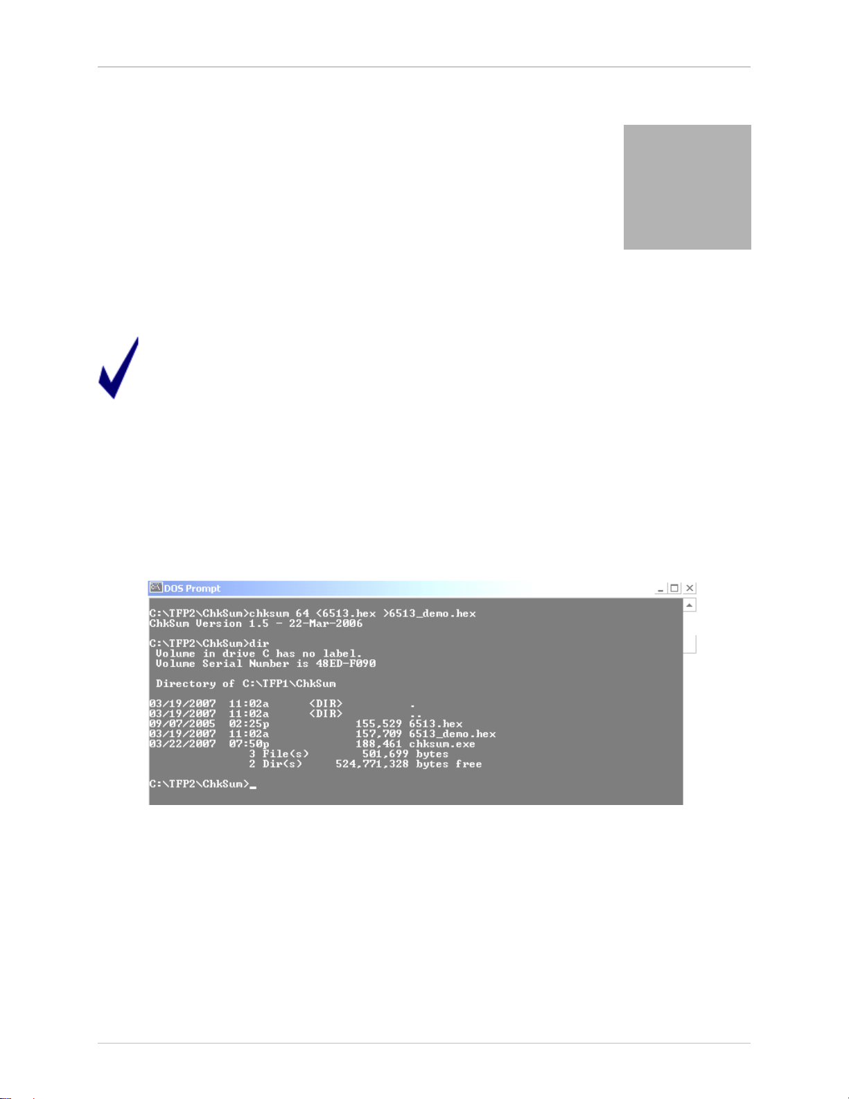
From the DOS Command prompt, inv ok e CHKSUM.EXE as follows:
chksum kb <infile.hex >outfile.hex where:
kb = desired file siz e, Mem or y Size S witch setting to be used during TFP2 downloading and
target programmi ng
infile = t ar get code hex file to be processed
outfile = processed t ar get code hex file to be downloaded to TFP2
The following fi gur e shows a typical invocation of CHKSUM.EXE:
Figure 2-1: CHKSUM.EXE Hex File Processing
The purpose of the CHKSUM utilit y is to or ganize the individual hex records into a contiguous “sequential
address increasing” structure. Some complier s produce non-sequ ential hex files. T he TFP2 assumes a
sequential file struct ur e. A non-sequential hex file downloaded to the TFP2 resul ts in missing bytes (the
missing bytes are the out -of-sequence hex records) in the target flash memor y (when the target is then
programmed wit h the TFP 2).
The CHKSUM.EXE utility m ay or may not ov er write the last four bytes of the downloaded target hex file
depending on whether these l oc ations are used or not.
Revision 2.3 7 of 36
Page 8
Flash Programmer Model TFP2 User’ s M anu al
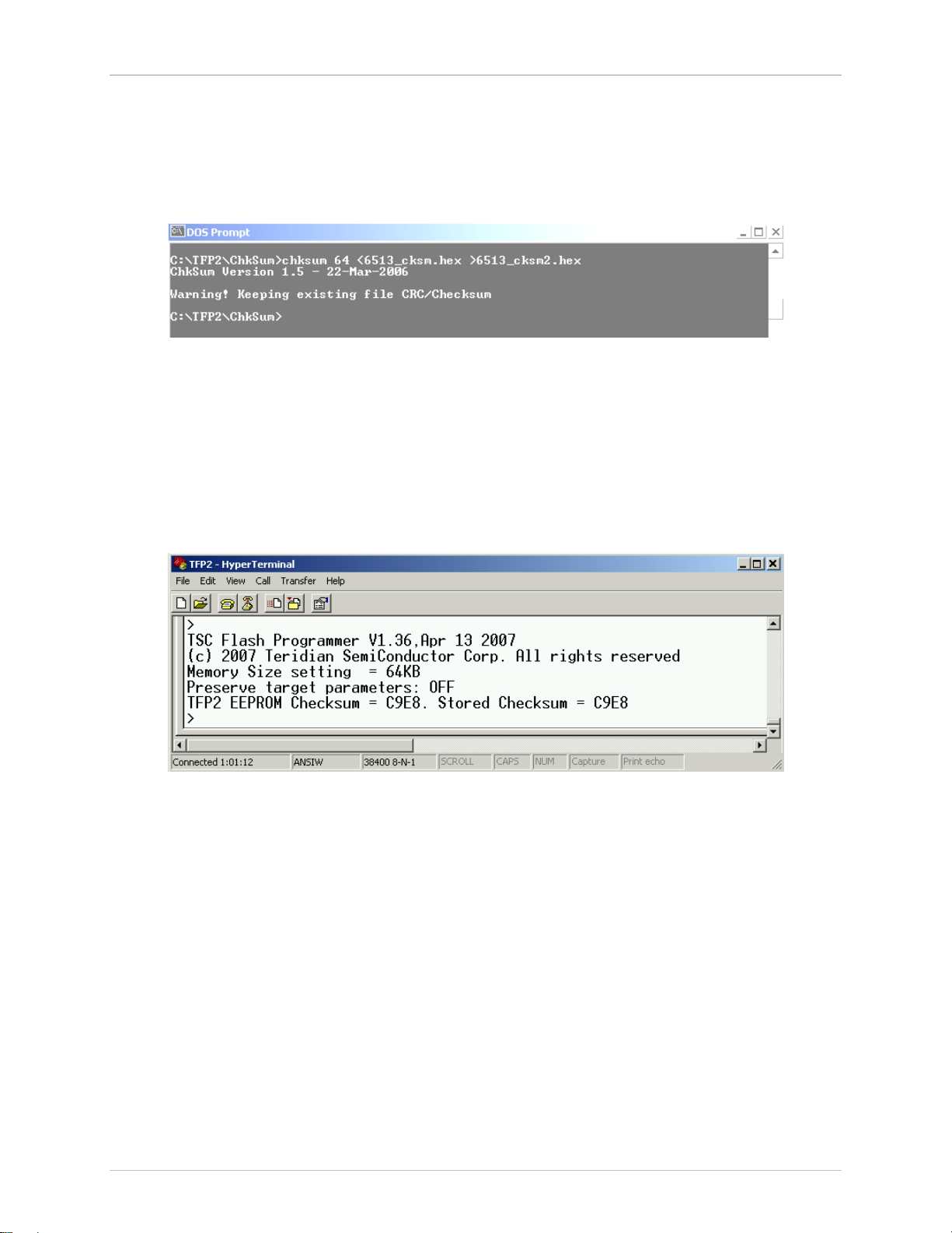
The following cases apply to using the CHKSUM.EXE utility:
1. If the last four byt es of the t ar get hex file are unused (0xFF), the CHKSUM.EXE uti lity will insert
its own calculated t wo byte CRC and two byte checksum.
2. If any of the last four byt es of the t ar get hex file are non-0xFF values, the CHKSUM.EXE utility
will NOT overwrite the four original values.
The CHKSUM.EXE utility displ ay s the following warning when it encounters non-0xFF values:
Figure 2-2: CHKSUM.EXE Warning Display
When programmi ng the target FLAS H m em ory, these last four bytes of the target hex file are transf er r ed
intact. Either the CHKS UM.E XE calc ulated CRC and checksum bytes are copi ed or the ori ginal target’s
hex data are copied. If the last t wo bytes of the target hex file are 0xFF (CHKSUM not used), t he TF P 2
overwrites the last two 0xFF bytes with its calculated checksum dur ing the Hyper-Terminal file Download
operation.
With HyperTerminal configured for serial COM port, 38400 baud, 1 stop bit, no parity, XON/X OF F ( refer to
Section 3.3 for serial communic ation setup information) the following inform ation is displayed upon
applying power to t he TFP2. Any generic termi nal emulation program will work. Howev er , the target hex
file download instr uc tions presented apply to HyperTerminal.
Figure 2-3: TF P 2 Powe r -Up Information Display
The Memory Size Switc h setting and the checksum of the current target fil e stor ed in the TFP2’s internal
EEPROM are displayed. An “I nv alid M em or y Size setting” m essage appears if the Memory Size Switch is
set to one of the invalid positions. Rotate the Memory Size Switch to a proper setting and re-apply power
to the TFP2 to update the Memory Siz e setting.
If the target hex file has non-FF values in any of the last four bytes, t he abov e power-on screen m ay
display a “TFP2 EEPROM verification er r or .” message. The displayed “TFP2 EEPROM Checksum =”
value and “Stored Checksum =” value will be different. This occurs when the stored check sum value
(from user’s target fi le) is derived from a different c hec ksum c alc ulation from what the TFP2 uses.
Therefore, the TFP 2 c annot confirm the EEPROM’s contents. Howev er, the chec k sum verification error
will not prevent the TF P 2 from programming a target board. The “TFP2 EEPROM Checksum =” value is
recalcul ated upon every power-on or system reset. Manual verification of the EEPROM’s contents
requires compari ng the TFP2 EEPROM Checksum value derived after the file download to subsequent
power-on recalculated checksum values. See Figure 2-8 for an example of a display ed c hec k sum value
after a file download.
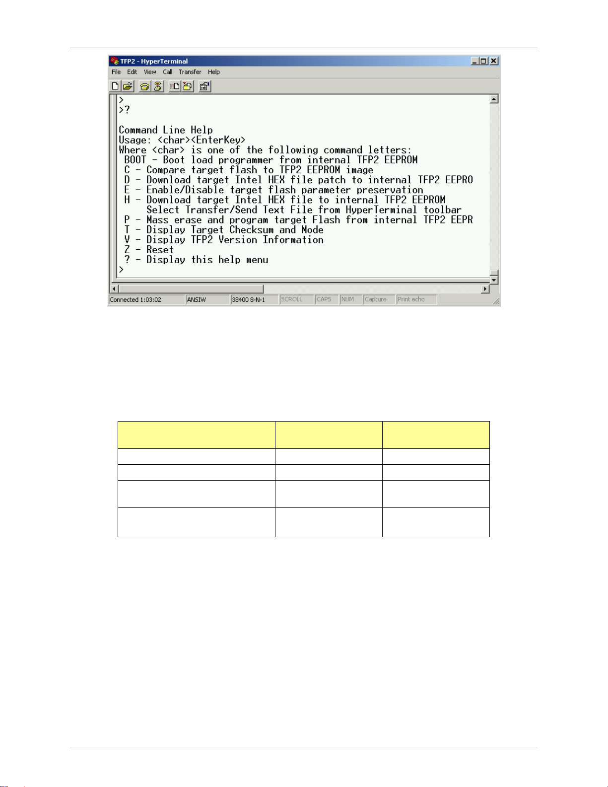
Upon pressing the “Ent er ” key , the “>” charac ter is displayed indicating the TFP2 acknowledges the PC’s
keyboard. Typing “ ?” followed by the “ E nter” key displays the Help Menu.
Revision 2.3 8 of 36
Page 9
Checksum
Flash Programmer Model TFP2 User’s Manual
Figure 2-4: TFP2 Help M enu
Commands C, E, T, V, Z and ? are single keystroke events (no further user acti on requi r ed until the TFP2
completes the int ended task). The D, H and P commands require additional user action and are
described in Section 2.6, Section 2.2, and Section 2.3, respectively. The BOOT command is a special
user action and is descri bed in Section 5.
The following t ables show the results of the last two words of the hex file after usi ng CHKS UM and after
downloading and program m ing using the TFP2. The referenced addresses assume use of a 64KB flash
memory configuration.
Initial Hex File Dat a File Address
0xFFFC
Hex Fi le with 0xF F 0xFFFF 0xFFFF
Hex File with non-0xFF CRC UserData 0xFFFF
Hex File with non-0xFF
Hex File with non-0xFF CRC
and non-0xFF Checksum
Table 2-1: CHKSUM Utility Addresses
Upon executing CHKS UM, the fi r st line displayed contains the CHKS UM versi on. Table 2-2 shows the
results of processing the above hex files with CHKSUM.
0xFFFF UserData
UserData UserData
File Address
0xFFFE
Revision 2.3 9 of 36
Page 10

Checksum
Target
Target
Program Verify Passes
Power-Up Verify Passes
Program Verify Passes
Power-Up Verify Passes
Program Verify Passes
Program Verify Passes
Power-Up Verify Fails
Program Verify Passes
Power-Up Verify Fails
Program Verify Passes
Power-Up Verify Fails
Power-Up Verify Fails
Flash Programmer Model TFP2 User’ s M anu al
Hex File Data after Using
CHKSUM
File Address
0xFFFC
CHKSUM v1.5
File Address
0xFFFE
Hex Fi le with 0xF F 0xFFFF Teridian
Checksum
Hex File with non-0xFF CRC UserData Teridian
Checksum
Hex File with non-0xFF
0xFFFF UserData
Hex File with non-0xFF CRC
UserData UserData
and non-0xFF Checksum
Table 2-2: CHKSUM Utility Output Data
The TFP2 Download Verify and P ower-Up Verify expects to read the Teridi an c hec k sum. For the
following ex am ples shown below, a Do wnload V er ify fail and Power-Up Verify f ail occurs because the
user data is preserv ed ( r ather than over-writing with the Teridi an v alues). A Download Verify fail and
Power-Up Verify f ail does not pr ev ent correct target memory programming ( these messages are
informati onal only). The Teridian checksum insertion (over-writing) m ay only occ ur when using CHKS UM
or during the TFP2 download (if 0xFF values are encountered).
The TFP2 programs into t he target memory what was previously downloaded (once downloaded, the l ast
two words do not change during pr ogr amming). The TFP2 then verifies the target memory to its internal
memory resulting in the correct PASS indication ev en when user data is present.
Target Data after Using TFP2
Hex Fi le with 0xF F 0xFFFF
Hex File with 0xFF after CHKSUM v 1.5 0xFFFF
Address
0xFFFC
Address
0xFFFE
Teridian
Checksum
Teridian
Checksum
Comments
Download Verify P asses
Download Verify P asses
Hex File with non-0xFF CRC UserData
Hex File with non-0xFF CRC after
CHKSUM v1.5 (includes UserData into its
Hex File with non-0xFF Check sum 0xFFFF UserData
Hex File with non-0xFF Check sum af ter
Hex File with non-0xFF CRC and non-0xFF
Hex File with non-0xFF CRC and non-0xFF
Checksum after CHKSUM v1. 5
Revision 2.3 10 of 36
Checksum)
CHKSUM v1.5
Checksum
Teridian
Checksum
UserData
Teridian
Checksum
0xFFFF UserData
UserData UserData
UserData
UserData
Table 2-3: CHKSUM Utility Data Dependency
Download Verify Fails
Power-Up Verify Fails
Program Verify Passes
Download Verify P asses
Power-Up Verify Passes
Download Verify Fails
Download Verify Fails
Download Verify Fails
Program Verify Passes
Download Verify Fails
Page 11
Flash Programmer Model TFP2 User’s Manual
2.2 TFP2 EEPROM DOWNLOAD
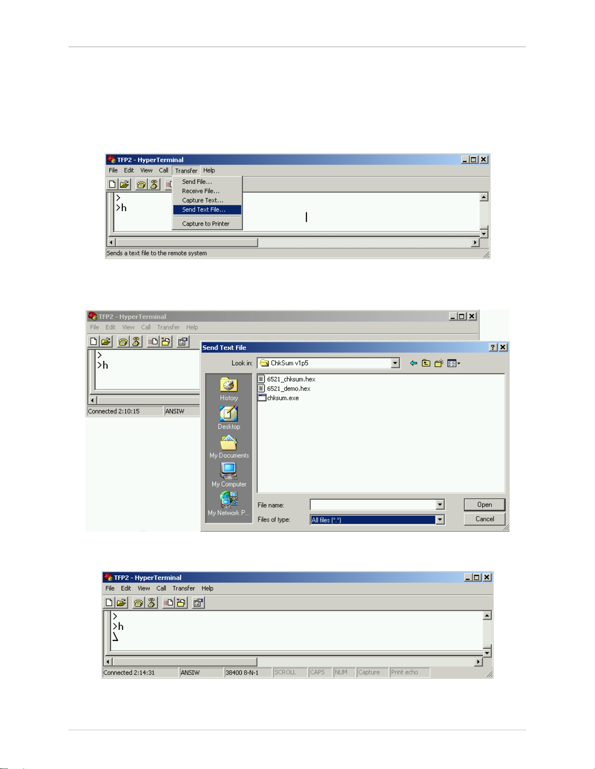
Transfer of the target’s code from a PC to the TFP2 begins with the “H” command. The target code file
must have been preprocessed using the CHKSUM.EXE utility pr ov ided on the enclosed diskette. Refer
to Section 2.1 for instructions on using CHKSUM.EXE. Use of any other format results in m alfunction and
download checksum er r or s.
After typing “H” followed by the “Enter” key, the cursor m ov es to the following line. Next, click on the
“Transfer” button and scroll down to “Send Text File” to select t he desired f ile to be downloaded.
Figure 2-5: TFP2 Intel Hex File Download to Internal EEPROM Command
Enable the “All files (*.*)” for file type and select your desired t ar get Intel Hex code file from the
appropriate sub-directory.
Figure 2-6: TFP2 Select Target Intel Hex Fil e
Upon clicking on “O pen” a rot ating prompt is displayed indic ating the file download is in progress.
Figure 2-7: TF P 2 D ow nload in Progres s
When the file download completes, the number of bytes transferr ed is displayed. A running CRC is
calculated during the file download for each byte received for programming into the TFP2 internal
Revision 2.3 11 of 36
Page 12

Flash Programmer Model TFP2 User’ s M anu al
EERPOM. The running CRC calculated during the file download is compar ed to the embedded CRCs of
the indivi dual byte r ec or ds within the hex file for appropri ate PASS and FAIL indication. Additi onally, the
appropriate green or r ed LE D is ill umi nated. The TFP2 EEPROM checksum calculation value is based
on the memory size switch setting and is displayed for future reference. The download transfer times
may vary from 15 minutes to 1 minut e for a 64 KB fil e size. The Microsoft
Windows 2000 Service Pak 4
or later affor ds the faster download time.
Figure 2-8: TFP2 Download Complete
Possible reasons for a FAIL indication upon downloading a fi le to the TFP2:
1. Downloaded file not Intel Hex format.
2. USB to RS-232 dongle communicati on pr oblem (i nc r ease Line del ay to 10 msec.).
3. USB to RS-232 dongle does not support XON/OFF .
4. XON/XOFF protocol f ailure, close and restart Hyper-Terminal.
5. Hex file not converted using the CHKSUM.EXE utility.
6. The following messages appear when the Memory Size Switch setting is too small for the
downloaded file.
Figure 2-9: TF P 2 D ow nload Fail due to Incorrect Memory Size Setting
Revision 2.3 12 of 36
Page 13

Flash Programmer Model TFP2 User’s Manual
2.3 TARGET FLASH MEMORY PROGRAMMING
Programming of t he target’s FLASH memory begins with typing “P” followed by the “Enter” key. The
green LED on the TFP2’s front panel blinks while the target FLAS H memory is being mass erased,
programmed and verified. The red LED will momentarily flash on at t he star t of pr ogr amming. Upon
completion of the target FLASH memory programming the following display appears. Additionall y , t he
green or red LED is illumi nated upon completion of the target F LASH mem ory progr amming.
Figure 2-10: T FP2 Target Mass Erase and Program Command
If the existing devic e’s securi ty bit is set, the TFP2 prompts for confirmation that programming is to
continue.
Figure 2-11: Existing Device’s Security Bit S et
Type an uppercase “Y” t o continue device programming.
Pressing the Program Button on the front panel of the TFP2 automati c ally proceeds with device
programming regar dless of the security bit setti ng.
Figure 2-12: Programming Overrides Security Bit
Revision 2.3 13 of 36
Page 14

Flash Programmer Model TFP2 User’ s M anu al
If the TFP2 cannot communic ate with the target board, a “Command Timeout” message appears.
Possible reasons for a Command Timeout indication upon programming the target board:
1. Power not provided to target board preventing TFP2 communication with target boar d.
2. Bad cable connecti ng TF P 2 to target boar d pr ev enting TFP2 communication with target board.
3. Malfuncti oning target board preventi ng TFP2 communication with target boar d.
4. TFP2 Programmers buil t bef or e J une 2011 m ay have timing issues with some 78M66xx devi c es.
Contact Teridian for further information.
NOTE: The TFP2 must be powered first before connecting the target board to the TFP2.
NOTE: The target’s watchdog timer must be enabled (V1 pin not connected to
V3P3) and the target’s I CE _E pin must be connect ed to the approp riate
TFP2 connector pin for target flash re-programming if the target’s secu rity
bit is set.
NOTE: Wrong Memory Size switch setting will result in a Verif ication Error FAIL message.
2.4 PREVIOUSLY PROGRAMMED DEVICE VERIFICATION
A previously programm ed dev ic e c an be c hec k ed against the cur r ently loaded image contai ned in the
TFP2. Use the “C” command to perform t his compar ison. The green LEDs are illuminated if the flash
contents of the dev ic e in the socket m atch the contents of the TFP2 EEPROMs.
Figure 2-13: Previously Programmed Devi ce Check
If the security bit is set, the target’s FLASH memory cannot be read. Therefore, the Compare result s will
fail as shown below. The red LEDs are ill umi nated indicating thi s condit ion.
Figure 2-14: Previously Programmed Devi ce Check with S ecuri t y Bit Set
Revision 2.3 14 of 36
Page 15

Flash Programmer Model TFP2 User’s Manual
2.5 DEVICE STATUS CHECK
The contents of a devic e may be read-bac k to display its current security bit setting and checksum. Use
the “T” command to perform t his read-back.
Figure 2-15: Device Checksum and Security Bit Status
If the security bit is set, the target’s FLASH memory cannot be read. Therefore, the Status results cannot
be displayed as shown below.
Figure 2-16: Device Checksum and Security Bit Status with Security Bit Set
2.6 CODE OR PARAMETER UPDATE
The TFP2 firmware typi c ally performs a block erase prior to programming the device’s flash memory.
Additionall y , t he TFP2 progr am s the entire address space of the flash m em ory. The “D” command all ows
for programming only a small portion of the target’s FLASH memor y, i.e. – code patch or parameters.
Use the “D” command to download a code patch or a parameter table to the TFP2 EEPROM without
erasing and reprogramming the entire TFP2 EEPROM memory. The memory loc ations to be
reprogrammed are read f r om the downloaded Hex File. F ollow the same instructions of Secti on 2.2
regarding select ing “Send Text File” menu option after typing the “D” command.
Use the “P” command or the PROGRAM button to program the target board’s FLASH m em ory wit h the
updated TFP2 EEPROM content s.
The TFP2 Power-Up checksum v erific ation expects to read the ori ginal Teridian checksum. The PowerUp checksum verification may fail due to the code change. A Power-Up Verify fail does not prevent
correct device m em ory progr amming (these messages are inf ormational only). Use the “T” command to
verify the current device checksum.
2.7 PARAMETER PRESERVATION PROGRAMMING
The TFP2 firmware typically performs a block erase prior to programming t he devi c e’s flash memory.
Additionall y , t he TFP2 progr am s the entire address space of the flash m em ory. Opti onally , the TFP2 can
reserve 4KB of flash memory for code or param eter tables.
Use the “E” command to toggle whether the 4KB is preserved or erased/over-written during the “P”
programming operation. The Parameter Mode status change is displ ay ed as shown below.
Revision 2.3 15 of 36
Page 16

Flash Programmer Model TFP2 User’ s M anu al
Figure 2-17: Paramet er M ode Selection
After setting the Par am eter Mode using the “E” command, programm ing can be initiated using the “P ”
command or by pressing the f r ont panel Program button.
When Parameter Mode preservation is enabled, the TFP2 progr am m ing operation copies the existing
parameter data f r om the target device. A bulk erase and reprogramming of t he target’s FLASH memory
is performed. The TFP2 then r estor es the pr ev iously copied parameter dat a star ting at its highest
address locati on. Parameter data is re-wri tten to decreasing address locations until all parameter data
locations have been r estor ed. If new code (non 0xFF data) is encountered ( above the lowest reserved
parameter address loc ation) the message “No parameters preserved” is displayed during the
programming operation.
The location of the 4KB par am eter space depends on the target device’s FLA S H m em ory siz e. The
TFP2 determines the tar get FLASH memory size from the front panel Mem or y Size switc h. The following
table shows the reserved address locations of param eter space for different m emory si z es.
Memory Size
Switch
8KB Not Used Not Used
16KB 0x2000 0x2FFF
32KB 0x5000 0x5FFF
64KB 0xD000 0xDFFF
128KB 0x0001:D000 0x0001:DFFF
256KB 0x0003:D000 0x0003:DFFF
Table 2-4: Parameter Space Address Locatio n
Usage of the above parameter space assumes new program code does not exist at the prev ious
parameter( s) address locations. The TFP2 also assumes that the param eters are stored as a contiguous
block. This block of paramet er s can be located anywhere within the reserved memory locations.
Locating the par am eters at the end of the Parameter Space allows for the progr am code to “ gr ow” i nto the
lower addresses of t he par am eter space.
The location of the conti guous parameter block is determi ned by searching for a non 0xFF data byte
beginning at the Par am eter Space “End Address” of the TFP2’s EEPROM im age. The address counter i s
decremented until a non 0xFF value is found. This locates the lowest address of the parameter data, the
“End Address” being the hi ghest addr es s.
Parameter
Space Start
Address
Parameter
Space End
Address
The TFP2 Power-Up checksum v erific ation expects to read the ori ginal Teridian checksum. The PowerUp checksum verification may fail due to the code change. A Power-Up Verify fail does not pr event
correct device m em ory progr amming (these messages are inf ormational only). Use the “T” command to
verify the current device checksum. The “T” command always includes the Parameter Space addresses
in its checksum calculation regardless of the Parameter Preservation Mode setti ng. However, the “C”
command operation varies with the Parameter Preservation Mode setting. The Parameter Space
addresses are incl uded in the comparison when Parameter Pr eservation Mode is OFF. Otherwise, the
Parameter Space addr esses are i gnor ed if Parameter Preserv ation Mode is ON.
The Parameter Mode status i s al so di spl ay ed in the power-up initialization messages.
Revision 2.3 16 of 36
Page 17

Flash Programmer Model TFP2 User’s Manual
Figure 2-18: Paramet er M ode Status
Revision 2.3 17 of 36
Page 18

Flash Programmer Model TFP2 User’ s M anu al
Revision 2.3 18 of 36
Page 19

3
Memory Size
PC
RS232
Flash Programmer Model TFP2 User’s Manual
3 TARGET CODE INITIALIZATION
Before the target’s FLA S H m em ory can be pr ogr ammed, the target code must be transf er r ed to t he TFP2
for internal storage. First configure the TFP2 for the proper mem ory siz e of t he target’s code. Rotate the
internal Memor y Size r otary switc h to the appropriate position. There is a black arrow on top of the rotary
switch shaft denoting the switch position. Only six of the eight switch positions are used. The other two
positions are not used. A blink ing red LED after applying power to t he TFP2 indicates one of these
unused positions is curr ently selected. Rotat e the Mem or y Size S witch to a proper setting and re-apply
power to the TFP2 to update the Memor y Size setting.
Selection Switch
Figure 3-1: Memo ry Siz e Con figu rat io n
Figure 2-2 shows the basic RS-232 c onnec tion of the TFP2 to a PC. Invoking a terminal emulator
program such as Micr osoft’s Windows 2000
for controlling the TFP2. Refer to Section 2 for instructions on using the user interface.
Figure 3-2: TF P2 RS-232 Connection to PC
HyperTerminal, displ ay s a simple text based user interf ac e
Revision 2.3 19 of 36
Page 20

Connector
Connector
Flash Programmer Model TFP2 User’ s M anu al
3.1 POWER SUPPLY CONNECTION
The TFP2 is supplied with a univ er sal A C/DC wall t r ansformer. Alternatively , t he TFP2 can be powered
by another external power supply. The TFP2’s power connector requires a 2.5 mm (inner diameter)
power plug. The center conductor is the +VDC and the outer conductor is Gr ound. Exter nal power
supply voltage range is +5VDC +/- 10% regulated. Maximum required power supply current is 200 mA.
NOTE: The TFP2 doe s not supply powe r at the Ta r ge t -LS and Target-HS connectors. Power must
be supplied to the target board separately. The TFP2 must be powered first before connecting the
target board to the TFP2.
3.2 RS-232 SERIAL CONNECTION
For connection of the DB 9 serial port to a PC, a straight cable must be used.
PC Pin
Male
2 RX 2
3 TX 3
5
Table 3-1: RS-232 Straight Cable Connections
PC
Function
Signal
Ground
TFP2 Pin
Female
5
3.3 SERIAL CONNECTION SETUP
After connecting the DB9 serial port to a PC, start the HyperTerminal application and create a session
using 38400 baud, 8 bits, no par ity, 1 stop bit, and XON/XOFF flow control. HyperTerminal can be found
by selecting Programs Accessories Communications from the Wi ndows
connection param eters are configured by selecting File Properties and then by pressing the Confi gur e
button. If the Configure button is not active, select Call Disconnect. Port speed and flow control ar e
configured under the General tab, and bit setti ngs are configured after pressing the Configure button, a s
shown in Figure 3-3.
start menu. The
Figure 3-3: Por t Speed, Port Bit Setup a nd Flow Control
Once, communic ation to the TFP2 is established, press the “E nter” k ey and the TF P 2 program pr om pt “>”
should appear. Typing “?“ displ ay s the TF P 2 pr ogr am help menu. Type “V“ to verify that the TFP2
program version is revision 1.00 or later.
Refer to Section 2 f or instructions on using the PC User Interfac e.
Revision 2.3 20 of 36
Page 21

4
Target-
LS
Target-
HS
Flash Programmer Model TFP2 User’s Manual
4 TARGET FLASH MEMORY PROGRAMMING
The TFP2 Flash Programm er connects to the target board via one of two connect or s:
1) The Target-LS connector pr ov ides connection using discrete wires.
Only use this interf ac e for TCLK frequenc ies of 10 MHz or less.
Figure 4-1: Target-LS Connection
2) The Target-HS connector utilizes the ADM-1 ribbon cable connect or .
Must use this interface for TCLK frequencies of 10 MHz or faster.
Figure 4-2: Target-HS Connection
These two connectors are hard wired together. They are not two separate i nterfaces (two different target
boards cannot be programm ed c onc ur r ently).
The Target HS interface must be used when programming 73S12xxF and 78M66x x dev ic es
regardless of the TCLK speed.
Revision 2.3 21 of 36
Page 22

1 3 5 2 4
6
Flash Programmer Model TFP2 User’ s M anu al
The target connector pin assignments are as follows:
Target-LS
Pin
1 Ground
2 TCLK Input
3 Ground
4 RESET Output
5 I CE E nable Output
6 RXTX Bi-Directional
Table 4-1: Target-LS Connector Pins
Figure 4-3: Target-LS Connector Pin Locations (looking at TFP2 endplate)
The TFP2 does not supply power at t he Target -LS c onnector . Power must be supplied to the target
board separately . T he TFP2 must be powered first before connecting the target board to the TFP2.
Target-LS Connect or part num ber s:
1. Connector Housing, 6 pin, 0.100
AMP 2-87977-8 (Digi-Key A25831)
Pin Function TFP2 I/O
2. Connector Pins, Crimp
AMP 102348-2 (Digi-Key A25943-ND)
Revision 2.3 22 of 36
Page 23

1
Ground
11
11
Ground
4
RESET
Output
14
14
Not Used
7
Ground
17
17
Ground
10
Not Used
20
20
Not Used
1 3 5 2 4 6 7 8 9
10
11
12
13
14
15
16
17
18
19
20
Flash Programmer Model TFP2 User’s Manual
Target-HS
Pin
2 I CE E nable Output 12 12 Not Used
3 Ground 13 13 Ground
5 Ground 15 15 Ground
6 TCLK Input 16 16 Not Used
8 RXTX Bi-Directional 18 18 Not Used
9 Ground 19 19 Ground
The TFP2 does not supply power at the Target -HS c onnector . Power must be supplied to the target
board separately . T he TFP2 must be powered first before connecting the target board to the TFP2.
Pin Function TFP2 I/O
Table 4-2: Target-HS Connector Pins
Figure 4-4: Target-HS Connector Pin Locations (looking at TFP2 endplate)
Target-HS
Pin
Pin Function TFP2 I/O
Cable length must not ex ceed 12 inches.
Target-HS ribbon cable part numbers:
1. 20-pin flat ribbon c able c onnec tor, 0.050
AMP 111194-4 (Digi-Key A29133-ND)
2. 20-conductor flat ribbon cable, 0.025
Temp Flex F30007S-20-025-85
4.1 STANDALONE PROGRAMMING
With the TFP2’s inter nal E EPRO M initialized with the target’s code as described in Section 3, and the
target board connected to the TFP2 via the Target-LS connector or the Target -HS connector, programming of the target’s flash memory may begin.
Figure 4-5: Standalone Configuration (shown with Target-HS cab le)
When power is applied at the DC IN connec tor, the yellow power indicator LE D is ill umi nated.
Programming of t he target FLASH Memory begins upon pressing the “Pr ogr am ” button. A momentary
push button press of 100 msec, not t o exceed 1 second i s required to commence programming. Mass
erase of the target’s FLA S H m emory is perf ormed first before programming of t he code begi ns. The
green Programmi ng/Pass LED blinks while programming is i n progress. Upon completion of
Revision 2.3 23 of 36
Page 24

Flash Programmer Model TFP2 User’ s M anu al
programming, the t ar get’s FLASH Memory contents are read back for verifi c ation. The green
Programming/Pass LED stops bl inking and turns on solid if t he target’s FLASH Memory content s are
verified as good. If v erific ation fails, the red Fail LED turns on solid. If the TFP2 cannot communicat e
with the target, the red F ail LE D turns on immediately. Communicati ons failure may result from no target
power, bad cable or fault y target board. No target FLASH Memory programmi ng will hav e oc c ur r ed when
communicati on has not been established. Either LED indicati on is cleared upon re-pressing the Program
button.
NOTE: The TFP2 must be powered first before connecting the target board to the TFP2.
NOTE: The target’s watchdog timer must be enabled (V1 pin not connected to
V3P3) and the target’s I CE _E pin (if avai lable on target device) must be
connected to the appropriate TFP2 connector pin for target flash reprogramming if the targ et’s security bit is set.
4.2 PC USER INTERFACE PROGRAMMING
Alternatively, manual programming may be performed using the PC User Interfac e. The green and red
LED indicators func tion as described above. The operational status information is also duplicated on the
PC’s screen. Refer to Section 2 for instructions on using the PC User Interface.
Figure 4-6: PC User Int erf ace Con f ig uration (shown with Target-HS cable fo r exampl e)
NOTE: The TFP2 must be powered first before connecting the target board to the TFP2.
Do not connect a PC to the TFP2 AND connect the TFP2 to a target board with any connection
to Line or Neutral. Equi pm ent damage will occur due to a Ground signal disparity or live
voltages.
4.3 ATE FACTORY AUTOMATION PROGRAMMING
Automated programming of the target’s FLASH Memory may be performed using the ATE connector.
The interface si gnals provided at the ATE connector allow a fac tory automation computer t o commenc e
programming and monitor the status of the progr amming results. The ATE interface cannot download
target code to the TFP 2’s i nternal EEPROM.
The TFP2 must be powered fir st before connecting the target board to the TFP2.
Revision 2.3 24 of 36
Page 25

1
RESETB
Input
Active LO reset to TFP2 processor.
with the target board.
Vih
+2.0V
+3.3V
Input high voltage
Parameter
Min
Max
Description
1
3
5
2 4 6 7 9 8 10
Flash Programmer Model TFP2 User’s Manual
The ATE connector pin assignments are as shown in Table 4-3:
ATE Pi n Pin Function TFP2 I/O Description
2 Ground
3 PROGRAM
4 Ground
5
6 Ground
7 PASS
8 Ground
9 FAIL
PROGRAM
ACTIVE
Input Active HI signal star ts target FLASH Memory programming. A
minimum 200 ms pulse is required.
Output Active Hi signal i ndic ates target FLASH Memory programming
in progress. De-assert PROGRAM upon PROGRAM ACTIVE
going high.
Output Active HI signal indic ates target FLASH Memory verifi ed to be
correct. PASS goes low when PROGRAM is re-asserted high.
PASS toggles Hi and LO during progr amming sequence.
Output
Active HI signal indicates target FLASH Memory failed
verification. FAIL goes low when PROGRAM is r e -asserted
high. FAIL toggles HI and LO if the TFP2 c annot communicate
10 Ground
Table 4-3: ATE Connector Pins
Figure 4-7: ATE Connector Pin Locations (looking at TFP2 endplate)
ATE Connector part num ber s:
1. Connector Housing, 10 pin, 0.100
AMP 3-87977-0 (Digi-Key A25835)
2. Connector Pins, Crimp
AMP 102348-2 (Digi-Key A25943-ND)
ATE interface Logic Level Specifications are given below:
Parameter Min Max Description
Vil 0.0V +0.5V Input low voltage
Table 4-4: ATE Connector Pin Input Voltage Thresholds
The RESET pin incorporat es a 1kΩ pull-up resistor to +3.3V.
The PROGRAM pin incorpor ates a 1kΩ pull-down resistor to Ground.
Revision 2.3 25 of 36
Voh
Vol 0.0V +0.45V @ 8 ma Output low voltage
Table 4-5: ATE Connector Pin Output Voltage Levels
+2.4V @ -2
ma
+3.3V Output high
voltage
Page 26

BEGIN
Memory
Set
HI
Is
HI
Is
HI
Yes
No, verify programmer inactive
Is
HI
No, wait for program sequence to
start
Yes
END
Program med a nd Ver i fi ed
END
Failed Verification
Yes
No
Turn-on po wer to
Set
LO
Is
LO
No, wait for programmer to com plete.
Yes
Flash Programmer Model TFP2 User’ s M anu al
The PROGRAM ACTIVE, PASS and FAIL outputs incorporate 62Ω series resistor s.
The flow chart shown i n Figure 3-9 details the programming sequence required of the ATE (must apply
power to TFP2 Flash Programmer before the sequence below begins).
target board
Target FLASH
ProgAct pin 5
PROGRAM pin 3
PROGACT pin 5
PROGRAM pin 3
Revision 2.3 26 of 36
PROGACT pin 5
PASS pin 7
Target FLASH Memory
Figure 4-8: Program Fl ow Chart
PASS pin toggles during pr ogr am sequence.
FAIL pin toggles if t he TFP2 cannot communicate
with the target board.
Target FLASH Memory
Page 27

5
Flash Programmer Model TFP2 User’s Manual
5 BOOT LOADER
The TFP2 Boot Loader enables the TF P 2 firm ware to be upgr aded in the field (rem ote location). The
Teridian Semic onduc tor provided TFP2 firmware file is first downloaded to the TFP2’s EEPROM.
Transfer of this revised firmware file from the TFP2’s EEPRO M to its loc al pr ogr am m em ory is performed
by typing “BOOT” at the command pr om pt. Detailed Boot Loader instructi ons are prov ided in the
following secti on.
5.1 BOOT LOADER OPERATION
Reprogramming (upgr ading) of the TFP2’s program mem or y is accomplished with the following steps:
1. Set front panel Memory Size switch to 64 KB position.
2. Download the new TFP2 firmware file using the “H” command. Follow the instructions described
in Section 2.2.
3. Update the TFP2 program memory usi ng the “BOOT ” command. The “BOOT” characters must
be upper case.
Figure 5-1: TFP2 Reprogram TFP2 Program Memory
4. To proceed with reprogr amming the TFP2, type an upper case “Y”. The green PASS led blinks
during the reprogr amming process. The TFP2 restarts it self onc e r epr ogr amming is complete.
Revision 2.3 27 of 36
Page 28

Flash Programmer Model TFP2 User’ s M anu al
Figure 5-2: TFP2 Boot Completion
If the internal TFP2 EEPROM c ontents are corrupted (checksum com pari son failure) or if the EEPROM
contents do not represent a T FP2 c ode file (user’s target code), the BOOT c ommand will NOT reprogr am
the TFP2. The current power-on screen is immediately displayed with no flashing PASS led when a
problem is encountered wit h the EEPROM contents.
Revision 2.3 28 of 36
Page 29

6
Flash Programmer Model TFP2 User’s Manual
6 STATUS INDIC ATIONS
6.1 NORMAL OPER ATION
Normal front panel LED oper ation:
5. Green LED blinks during target FLASH memory programmi ng and v erific ation.
6. Green LED on 100% when target FLASH mem or y verified as good.
7. Red LED never on during norm al operation.
Normal ATE status signal operation:
1. ProgramActiv e pin high dur ing target FLASH memory programming and verification.
2. PASS pin toggles HI and LO duri ng target FLASH memory programming and verific ation.
3. ProgramActiv e pin low upon completion of target FLASH memory verification.
4. PASS pin high when target FLA S H memory verified as good.
5. FAIL pin never high during normal operation.
6.2 ERROR CONDITIONS
Front panel Red LED error codes:
1. Red LED blinks after power-on – I nc or r ec t Mem or y Switch sett ing: either position 6 or 7 selected.
2. Red LED on 100% after TFP2 download – TFP2 download CRC failed.
3. Red LED on 100% immediately upon Tar get programming – Target not responding upon
attempted progr amming.
4. Red LED on 100% after power-on – TFP2 does not power-up correctly.
5. Red LED on 100% after programming – Target FLASH memory fails verification.
ATE FAIL status signal err or c odes:
ProgramActiv e pin LO and FAI L pin HI imm ediately - Target not responding upon att em pted
programming.
ProgramActive pin LO and FAIL pin HI after ProgramActiv e was HI- Target FLASH memory fails
verification.
Revision 2.3 29 of 36
Page 30

Flash Programmer Model TFP2 User’ s M anu al
Revision 2.3 30 of 36
Page 31

7
Flash Programmer Model TFP2 User’s Manual
7 TFP2 HARDWARE SPECIFICATIONS
Case Dimensions
Dimensions 6.0” x 2.5” x 1.5”
Weight 0.35 lbs.
Environmental
• Operating Temperature +10°…+50°C
• Storage Temperature -40°C…85°C
Power Su pp ly
Supply Voltage +5VDC +/- 10% regulated
Supply Current 200 mA max
Cable Plug 2.5 mm Diameter
ATE Connector
Input Voltage Lo 0.0V to +0.5V
Input Voltage Hi +2.0V to +3.3V
Output Voltage Lo +0.45V max @ 8 mA
Output Voltage Hi +2.4V min @ 2 mA
Target Connector
Input Voltage Lo 0.0V to +0.5V
Input Voltage Hi +2.0V to +3.3V
Output Voltage Lo +0.45V max @ 8 mA
Output Voltage Hi +2.4V min @ 2 mA
TCLK Frequency 10 MHz to 48 MHz
Revision 2.3 31 of 36
Page 32

Flash Programmer Model TFP2 User’ s M anu al
Revision 2.3 32 of 36
Page 33

8
Flash Programmer Model TFP2 User’s Manual
8 TROUBLESHOOTING
Proper function of t he TFP2 with the target IC depends on many factor s. These factors are:
• Cable length and cable quality
• S ignal termination
• Target board and target I C function
• M atch between selected flash program size and target flash size
When the programming pr oc ess seem s to f ail, it is useful to watch the feedback messages from the TFP2
via HyperTerminal. Using the C and/or T commands it can be determi ned quic kl y if t he issue is with t he
communicati on link or somewhere el se.
8.1 COMMUNICATION ERRORS
The typical response of the TFP2 to a communication error when issuing t he C c ommand looks as
follows:
>C
Comparing Target Flash to TFP2 EEPROM image
Command timeout.
Command timeout.
FAIL
>
The response to the T command will look as follows when the communication link is interrupted:
T
Command timeout.
>
Likely causes for c ommunication link issues are:
• Cable length – try to keep the cable length below 25 cm (10 inches)
• Cable quality – proper multiple grounding and strai ght cables without loops are preferred. Try to
use the original ribbon c able with an adapter to the target progr amming connector, if necessary.
• If the TFP2 and the PC connected to it have a different ground potential t han the target, ground
loops can occur. In that c ase, try to use an isol ated supply for the target.
• Termination – in-li ne r esi stor s, pull-up resistors (if used) and by pas s capacitors should be included in the target schematics in the same way as implemented on the Teri dian Demo Boards.
Consult the Demo Board schematics for comparison.
• Target board power – 3.3 VDC must be supplied to the target IC.
• Target oscill ator – ensure t hat the crystal is oscillating at 32. 768 k Hz using an osci lloscope. In
many cases, board contami nation or moisture can prevent the oscillator from functioning properly.
• ICE_E not pulled high – this pin, if available on the t ar get I C, must be pulled high.
• V 1 pin for 71M651x target ICs – for this IC family, the V1 pin must be pulled up to 3.3 VDC to dis-
able the internal watchdog timer.
• St uck RESET pin – the communication link will fail if this pin is tied to the active potential.
• S ome older TFP2 units may have timi ng issues when pr ogr am m ing 78M66xx devices. See Secti on 2.3.
Revision 2.3 33 of 36
Page 34

Flash Programmer Model TFP2 User’ s M anu al
8.2 VERIFICATION ERRORS
A typical dialog inv olv ing a verification error i s shown below. I n this case, the communication between
TFP2 and the target IC was establi shed, but the programmed target image had at least one error, which
was discovered duri ng the verify process.
>P
Programming Target Flash
Verifying Target Flash
Verification error.
FAIL
>
Likely causes for v erification issues are:
• Communication issues can look like a verification error if the signal quality and timing is marginal
– check the items listed above under Communication Errors.
See the hints given in Section 8.3.
• A n em ulator port signal is also connect ed to an LCD pin on the target board resulting in a
corrupted signal – pr ov ide a jum per that c an isol ate the LCD pin from the emulator signal(s)
during the flash program m ing process.
• Mismatch between selected target flash size and actual target flash size – check the setting of the
Memory Size Selection Switch and compare the file size with t he flash size given in the target IC
data sheet. For example, the 71M6534 has a flash size of 128 KB whereas the 71M6534H has a
flash size of 256 KB.
• M ismatch between linked t ar get fi le size and actual target flash size – check the li nk er settings
and linker report files.
• File error – check the target file loaded into the TFP2. Reload the file, if necessary.
8.3 CABLE ISSUES AND MARGINAL TIMING
Cable issues and marginal timing can manifest them selves as intermittent communication errors and/or
verification errors. If the methods listed in the previous section Verific ation Errors do not help, a few unconventional fixes can be tried:
• Raising the board volt age to 3.6 VDC.
• A dding a resistor of 10 kΩ between E_RXTX and V3P3.
8.4 FILE LOAD ERRORS
File load errors can occ ur when att em pting to load the target image fil e into t he TFP2 using
HyperTerminal. USB-to-serial converters sometim es misinterpret the XON/XOFF control sequences used
for flow control. These cases manifest themselves in stuck file loads or corr upted target images. The
solution is to move to a PC with a true seri al interface (COM port).
Revision 2.3 34 of 36
Page 35

Part Description
Order Number
9
Flash Programmer Model TFP2 User’s Manual
9 ORDERING INFORMATION
The following t able lists the or der number used to identify the TFP2 Flash Programmer.
Tabl e 9-1: Order Number
Flash Programmer Model TFP2 80515-FPBM-TFP2
Revision 2.3 35 of 36
Page 36

Flash Programmer Model TFP2 User’ s M anu al
Revision 2.3 36 of 36
 Loading...