

Page 1
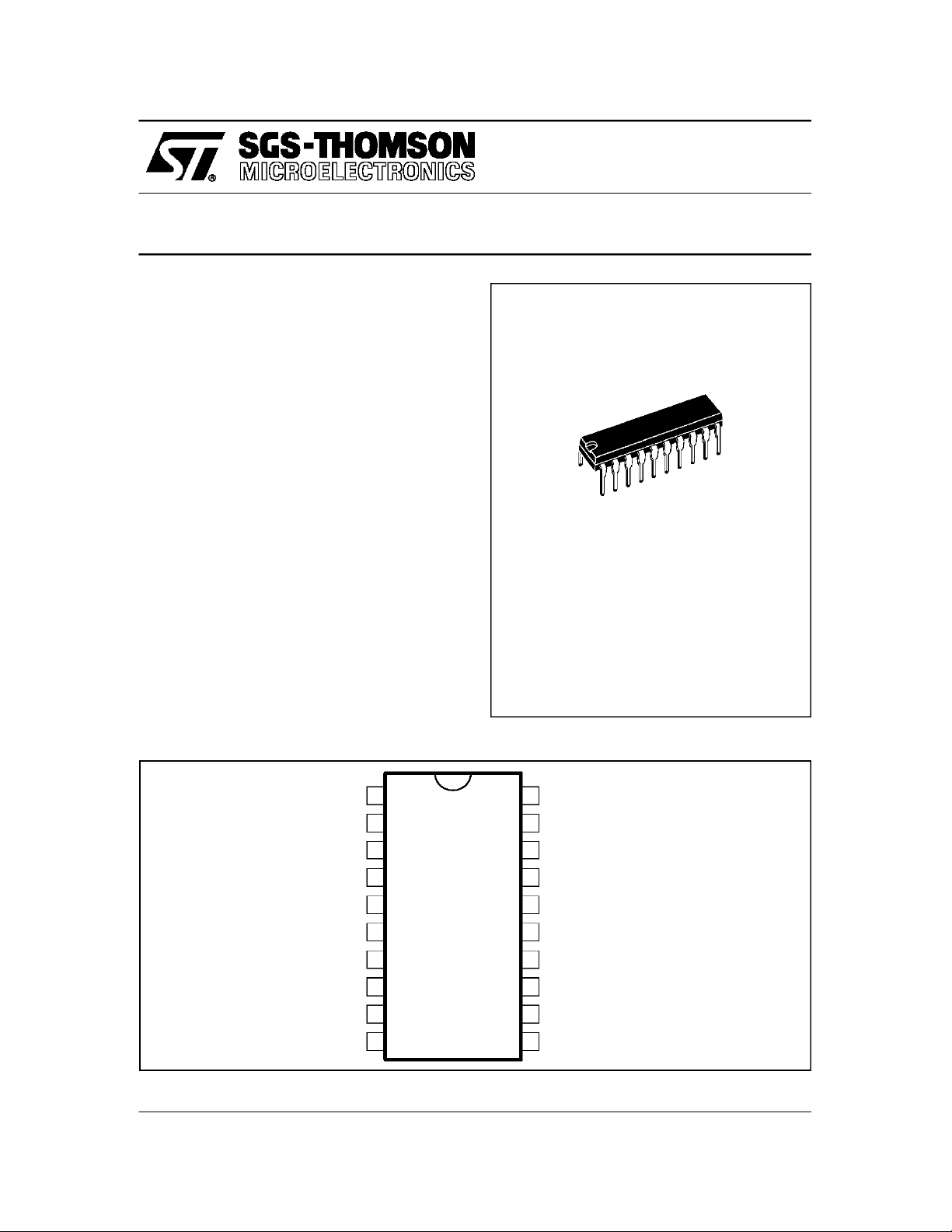
BUS-CONTROLLED VIDEO MATRIXSWITCH
.
15MHz BANDWIDTH
.
CASCADABLE WITH ANOTHER TEA6417
(INTERNAL ADDRESS CAN BE CHANGED
BY PIN7 VOLTAGE)
.
8 INPUTS (CVBS,RGB,MAC, CHROMA...)
.
6 OUTPUTS
.
POSSIBILITYOF MACOR CHROMASIGNAL
FOR EACH INPUT BY SWITCHING-OFFTHE
CLAMP WITH AN EXTERNAL RESISTOR
BRIDGE
.
BUS CONTROLLED
.
6.5dB GAIN BETWEEN ANY INPUT AND
OUTPUT
.
- 60dBCROSSTALK AT3.58MHz
.
FULLYESD PROTECTED
DESCRIPTION
The main function of the TEA6417 is to switch 8
videoinput sources on the 6 outputs.
Each output can be switched to only one of the
inputs whereas but any same input may be connectedto several outputs.
Alltheswitchingpossibilitiesarecontrolledthrough
2
the I
C Bus.
TEA6417
DIP20
(Plastic Package)
ORDER CODE : TEA6417
PINCONNECTIONS
May 1996
INPUT
DATA
INPUT
CLOCK
INPUT
INPUT
PROG
INPUT
V
CC
INPUT
1
2
3
4
5
6
7
8
9
10
20
19
18
17
16
15
14
13
12
11
INPUT
GROUND
OUTPUT
OUTPUT
OUTPUT
OUTPUT
OUTPUT
OUTPUT
POWER
DECOUPLING
INPUT
6417-01.EPS
1/7
Page 2
TEA6417
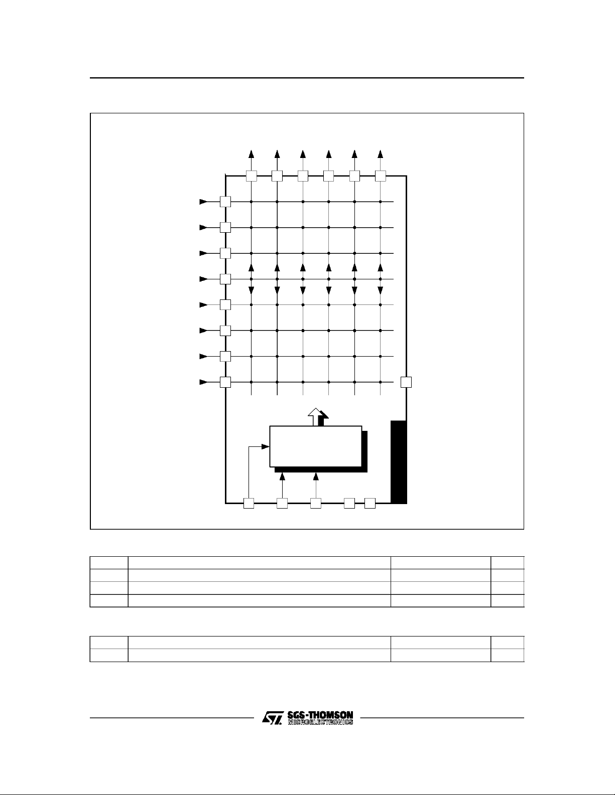
BLOCK DIAGRAM
CVBS
(MAC/DEC)
CVBS
(PERI PLUG1)
CVBS
(AMTUNER)
MAC SIGNAL
(AMTUNER)
CVBS
(PERI PLUG2)
CVBS
(FMTUNER)
MAC SIGNAL
(FMTUNER)
SYNCHRO
(TTX/BTX)
PERI
PERI
TV1
TV2
18 17 16 15 14 13
1
3
5
6
8
10
11
20
TTX
LUMA
CHROMA
POWER
PIP
MAC
DEC.
POWER
12
DECOUPLING
T
BUS
DECODER
E
A
6
4
1
7
274
DATA GNDCLOCK V
PROG
919
CC
ABSOLUTEMAXIMUM RATINGS
Symbol Parameter Value Unit
V
T
T
Supply Voltage (Pin 9) 13 V
CC
Operating Ambient Temperature Range 0 to +70
A
Storage Temperature Range -20 to +150
stg
THERMALDATA
Symbol Parameter Value Unit
R
th(j-a)
Junction-Ambient Thermal Resistance 80
2/7
o
o
C
o
C
C/W
6417-02.EPS
6417-01.TBL
6417-02.TBL
Page 3
TEA6417
ELECTRICALCHARACTERISTICS
T
=25oC,VCC= 10V , R
A
Symbol Parameter Min. Typ. Max. Unit
V
I
CC
INPUTS
OUTPUTS (V
2
C BUS INPUT : DATA,CLOCK, PROG (Pins 2 - 4 - 7)
I
Supply Voltage (Pin 9) 8 10 11 V
CC
Power Supply Current (without load on outputs ; VCC=10V) 20 30 40 mA
Maximum Signal Amplitude (CVBS signal) 2 V
Input Current (per output connected,input voltage = 5VDC)
(this current is X6 when alloutputs are connected on the input)
DC Level 2.8 3.1 3.4 V
=1VPPfor all dynamic tests) Pins 13 - 14 - 15 - 16 -17 - 18
IN
Dynamic 4 4.8 V
Output Impedance 25 50 Ω
Gain 5.5 6.5 7.5 dB
Bandwidth
-1dB attenuation
-3dB attenuation
Crosstalk
f = 3.58MHz
f = 5MHz
DC level 3.3 3.6 3.9 V
Threshold Voltage 1.5 2 3 V
LOAD
= 10kΩ ,C
= 3pF (unless otherwisespecified)
LOAD
13µA
710
15
-60
-55
-50 dB
PP
PP
MHz
MHz
dB
6417-03.TBL
GENERALDESCRIPTION
ThemainfunctionoftheICistoswitch8videoinput
sourceson 6 outputs.
Each output can be switched on only one of each
input. On each input an alignment of the lowest
levelof the signal ismade (bottomof synch.top for
CVBS orblack levelfor RGB signals).
Each nominal gain betweenany input and output
is 6.5dB. For D2MAC or Chroma signal the alignment is switched off by forcing, with an external
resistorbridge, 5 V
on the input.Each input can
DC
be usedas a normal inputoras a MACor Chroma
input (with externalresistor bridge). All the switching possibilitiesare changed through the BUS.
Driving75Ω load needsan external transistor.
It is possibleto have the same input connectedto
severaloutputs.
The starting configuration upon power on (power
supply: 0 to 10V) is undetermined.
In this case, 6 words of 16 bits are necessary to
determineone configuration.In other case,1 word
of 16 bitsis necessarytodetermineoneconfiguration.
3/7
Page 4
TEA6417
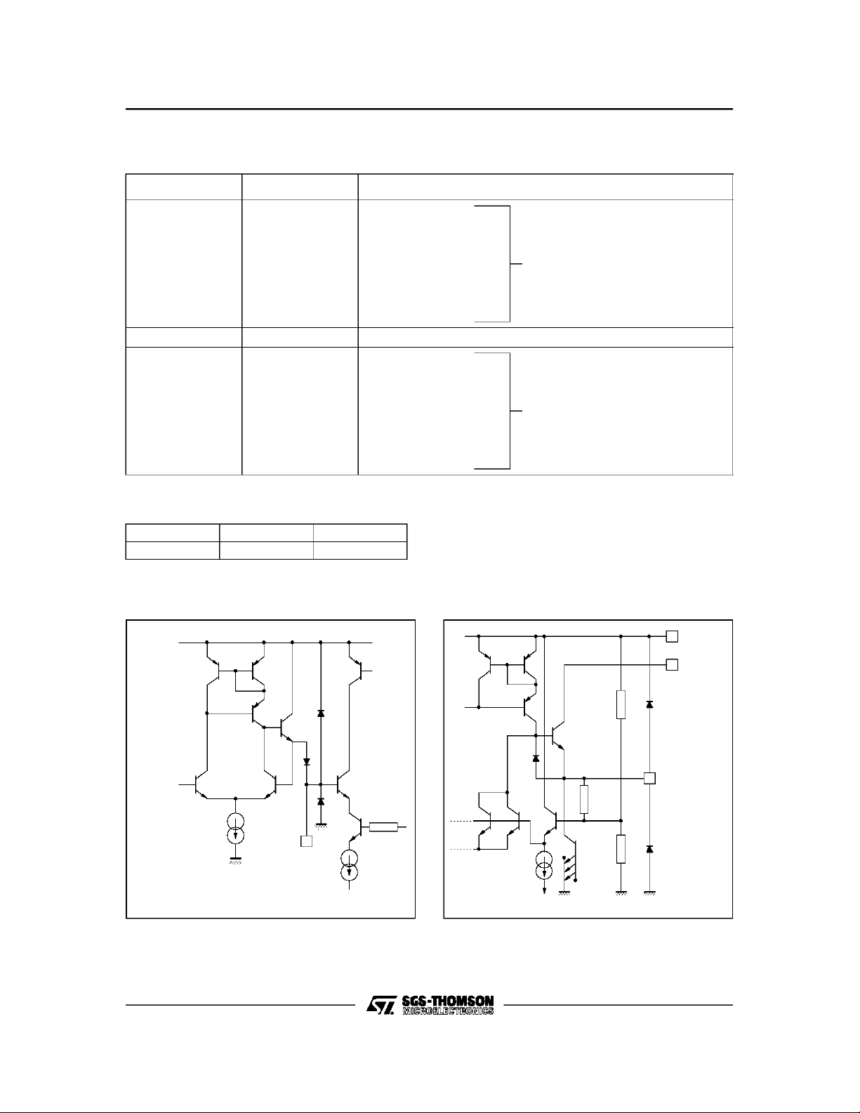
BUS SELECTIONS (I
2
C-BUS)
2 nd byte of transmission
ADDRESS
MSB
00000 XXX pin 18
00100 XXX pin 14
00010 XXX pin 16
00110 - - - Not used
00001 XXX pin 17
00101 XXX pin13
00011 XXX pin 15
00111 - - - Not used
00XXX 000 pin5
00XXX 100 pin8
00XXX 010 pin3
00XXX 110 pin20
00XXX 001 pin6
00XXX 101 pin10
00XXX 011 pin1
00XXX 111 pin11
DATA
LSB
Selected Output
Output is selected by
address bits
Selected Input
Input is selected by
data bits
Example:00100 101 connectspin 10(input)to pin 14 (output)(equals 25 in hexadecimal)
Adressbyte (1st byte of transmission)
96 1001 0110 When pin PROG is connected to ground
92 1001 0010 When pin PROG is connected to V
CC
6417-04.TBL
6417-05.TBL
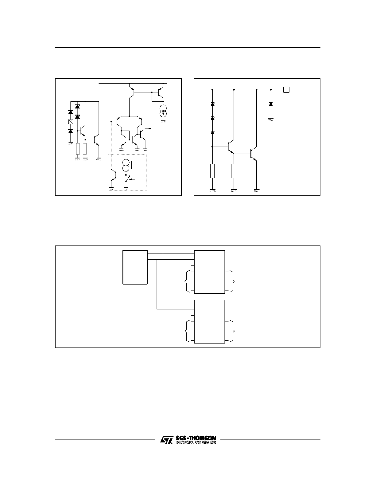
IN / OUT PIN CONFIGURATION
Figure 1 : Input Configuration
0.36 V
CC
Pins 1-3-5-6
8-10-11-20
4/7
6 times
Figure 2 : OutputConfiguration
9
V
V
CC
Ω
14k
x3
Ω
7k
Ω
8 NPN transistors
6417-03.EPS
11k
Output
CC
Power
12
V
CC
All video
outputs
Pins 13-14-15
16-17-18
6417-04.EPS
Page 5
IN / OUT PIN CONFIGURATION (continued)
Figure 3 : Bus I/OConfiguration
Pins
2-4-7
20kΩ 150Ω
V
REF
2
to I L
part
*
V
CC
250µA
Figure 4 : VCCPin Configuration
V
CC
TEA6417
Pin 9
ACK
* For Pin 2
(DATA) only
USE WITH AN OTHER TEA6417
The programmationinput (PROG) permitstooperate withtwo TEA6417inparalleland toselectthem
independantlythrough the I
2
C-BUSwithout modi-
Figure5
µP
logical ”0”
Video
Inputs
logical ”1”
Video
Inputs
20kΩΩ
6417-05.EPS
150
fying the adress byte. Consequently, the switch
capabilities are doubled or IC1 and IC2 can be
cascaded.
PROG
IC1
Video
Outputs
PROG
IC2
Video
Outputs
6417-06.EPS
6417-07.EPS
5/7
Page 6
TEA6417
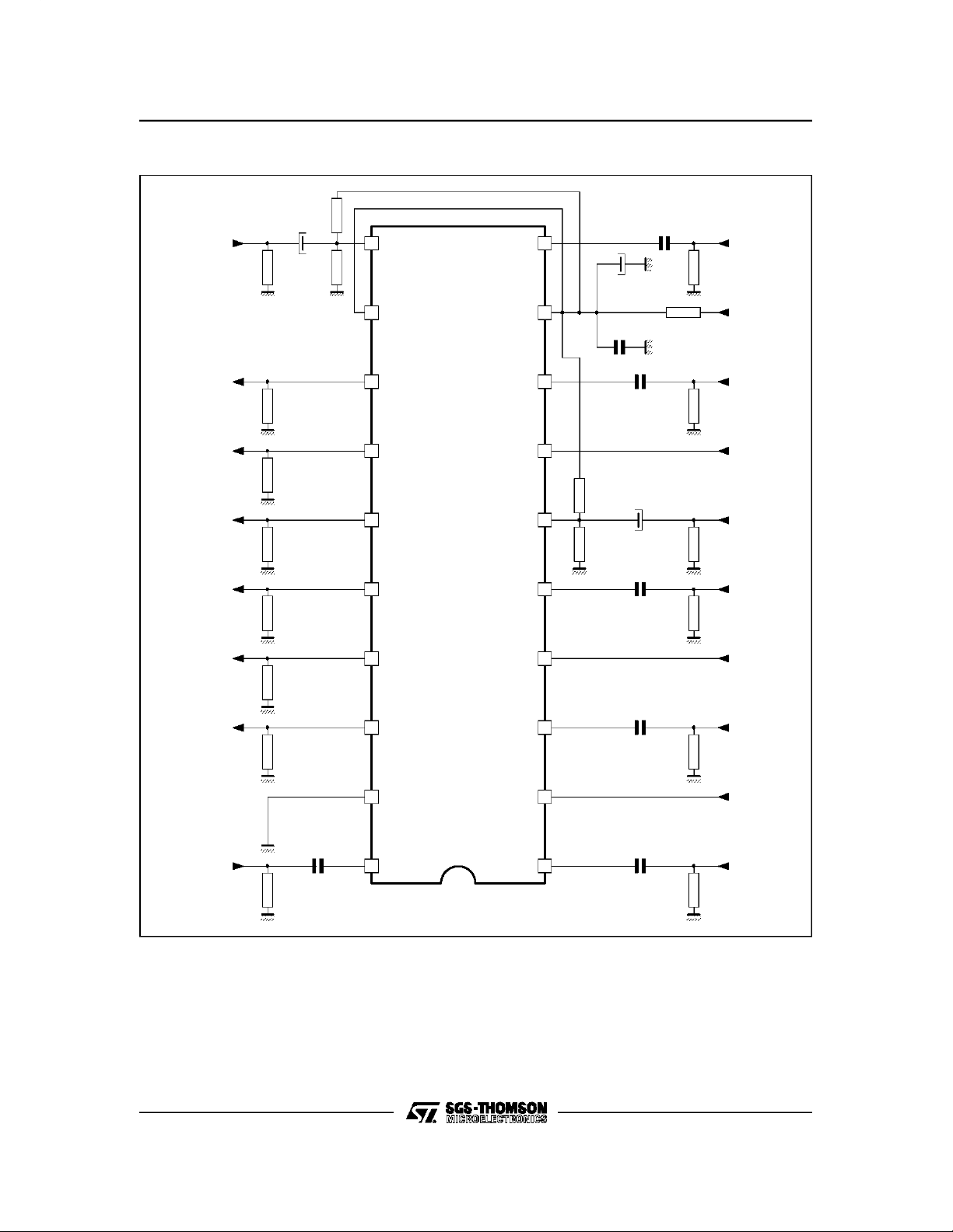
TYPICALAPPLICATION
MAC
100kΩ
22µF 220nF
11
68kΩ75kΩ
10
100
µF
75k
CBVS
Ω
CVBSOUTPUT
CVBSOUTPUT
CVBSOUTPUT
CVBSOUTPUT
YOUTPUT
C OUTPUT
12
V
Power VCC10V
CC
13
10kΩ
14
10kΩ
T
E
15
10kΩ
16
10kΩ
A
6
4
1
9
220nF
22
µF
220nF
10Ω
75kΩ
75kΩ
75kΩ
220nF
8
7
Ω
100k
6
68kΩ
5
7
17
10kΩ
18
10kΩ
4
220nF
3
75kΩ
CBVS
PROG (BUS)
C
Y
CK (BUS)
CVBS
19
20
75kΩ
2
220nF220nF
1
CROSSTALKIMPROVEMENT
Whenany inputis not used, it must be bypassedto ground through a220nF capacitor.
6/7
DA (BUS)
CVBSCVBS
75kΩ
6417-08.EPS
Page 7
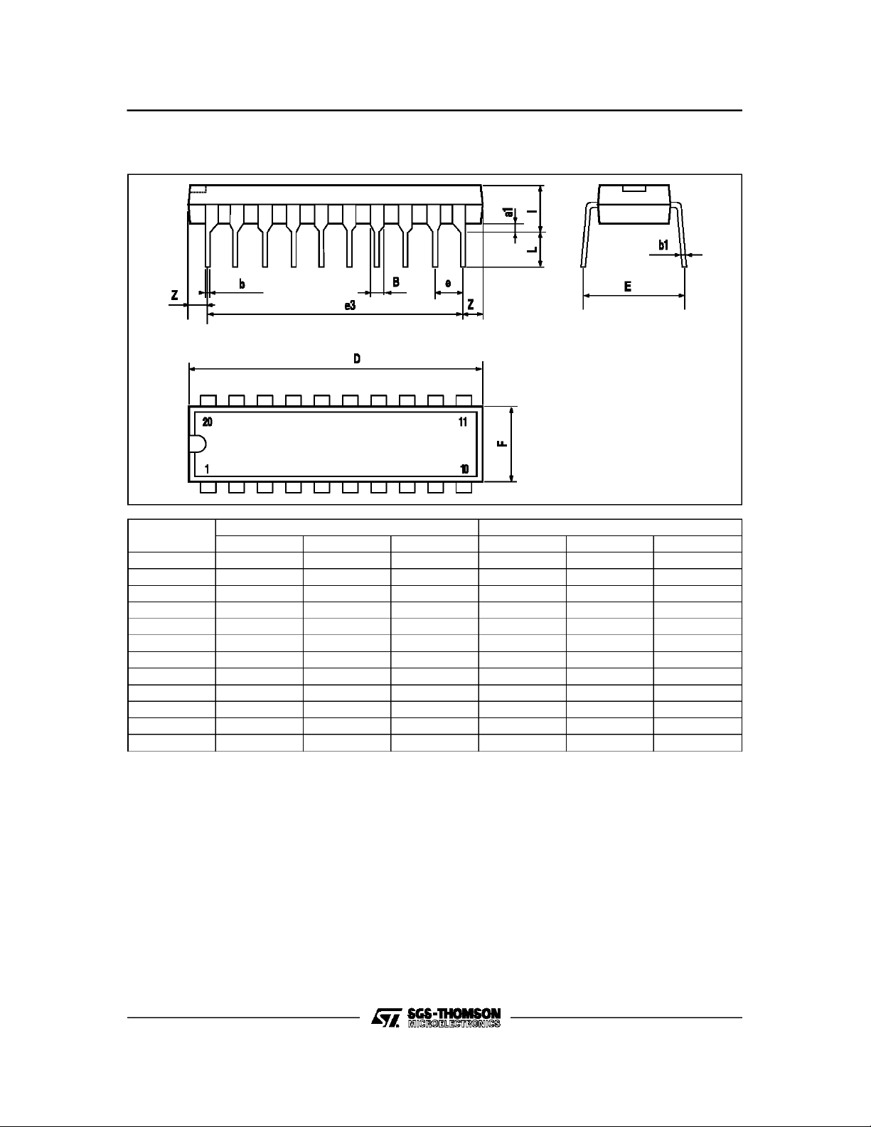
PACKAGEMECHANICALDATA
20 PINS– PLASTICDIP
TEA6417
PM-DIP20.EPS
Dimensions Millimeters Inches
Min. Typ. Max. Min. Typ. Max.
a1 0.254 0.010
B 1.39 1.65 0.055 0.065
b 0.45 0.018
b1 0.25 0.010
D 25.4 1.000
E 8.5 0.335
e 2.54 0.100
e3 22.86 0.900
F 7.1 0.280
I 3.93 0.155
L 3.3 0.130
Z 1.34 0.053
Information furnishedis believed tobe accurate andreliable. However, SGS-THOMSON Microelectronics assumes no responsibility
for the consequences of use of such information norforany infringement ofpatents or other rights of third parties which may result
from its use. No licence is granted by implication or otherwise under any patent or patent rights of SGS-THOMSON Microelectronics.
Specifications mentioned in this publication are subject to change without notice. This publication supersedes and replaces all
information previously supplied.SGS-THOMSON Microelectronics productsare not authorized for useas critical components in life
support devices or systems without express written approval of SGS-THOMSON Microelectronics.
1996 SGS-THOMSON Microelectronics - All Rights Reserved
Purchase of I
2
I
C Patent. Rights to use these components ina I2C system, is granted provided that the system conformsto
Australia -Brazil -Canada - China - France - Germany- HongKong - Italy - Japan - Korea- Malaysia - Malta - Morocco
The Netherlands - Singapore - Spain - Sweden - Switzerland - Taiwan - Thailand - United Kingdom - U.S.A.
2
C Components of SGS-THOMSON Microelectronics, conveys a license under the Philips
2
the I
C Standard Specifications as defined by Philips.
SGS-THOMSON Microelectronics GROUP OF COMPANIES
DIP20.TBL
7/7
 Loading...